Separating spins by dwell time of electrons across parallel double δ-magnetic-barrier nanostructure applied by bias
2022-01-23SaiYanChen陈赛艳MaoWangLu卢卯旺andXueLiCao曹雪丽
Sai-Yan Chen(陈赛艳), Mao-Wang Lu(卢卯旺), and Xue-Li Cao(曹雪丽)
College of Science,Guilin University of Technology,Guilin 541004,China
Keywords: parallel double δ-magnetic-barrier nanostructure, bias, dwell time, spin polarization, temporal spin splitter
1. Introduction
With the development of modern material growth technology, nano-scaled magnetic materials can now be deposited on the surfaces of semiconductor heterostructures experimentally.[1]The movement of high-mobility twodimensional electron gas (2DEG) embedded in the interface of semiconductor heterostructure can be controlled by an inhomogeneous magnetic field. Such a semiconductor heterostructure includes the so-called magnetic modulation semiconductor nanostructures (MMSN),[2]such as magnetic barriers (MB), magnetic traps, and magnetic superlattices. The MMSN is a small quantum system composed of semiconductor and magnetic materials. Beside the advantages of small size, low dimensionality, and local magnetic confinement,the MMSN has abundant physical properties, such as magnetic edge states,[3]wave-vector filtering,[4]magnetoresistance resonance,[5]giant magnetoresistance (GMR),[6,7]and spin polarization (SP).[8,9]These physical properties can be used to design new types of nanoelectronics devices, such as spin filters,[10]GMR devices,[11]momentum filters,[12]and spatial spin filters.[13]Therefore, the study of electron-spin transport characteristics in MMSN has attracted the great research interest.[14-20]
Two methods are used to study the electron-spin transport properties in MMSNs. The first method is to use the spin filtering of an MMSN,which gives rise to the electron-spin filter.When electron tunneling through the MMSN,the electron spin in a certain direction is suppressed,and the SP of electrons in semiconductor is realized.[21-25]The second method used to realize SP is to use the Goos-H¨anchen (GH) effect for electron beam in MMSN,i.e., spatially separating electron spins by GH displacement when electron beam traverses an MMSN,that is,the semiconductor nanostructure is devised as a spatial spin filter.[26-30]Meanwhile, another method is used specifically for separating electron spins in time dimension. This method of separating electron spins is to utilize different transmission times of electrons tunneling through the MMSN.The transmission time can help understand the dynamic response process of electronic device. Importantly, we can find a new way to realize the SP,that is,to separate electron spins in time dimension for injecting spin-polarized electrons into semiconductor. In 2002, Zhaiet al.[31]took the square MB MMSN for example and studied the transmission time of electrons in the MMSN.They used the group velocity method to calculate the group delay time of electrons. One year later,Xuet al.[32]calculated the phase delay time inδ-MB MMSN by using the stationary phase method,and put forward the idea of using the transmission time of electrons to separate spins in time dimension. However, in quantum mechanics, time is not an operator. Therefore, the measurement of time is still controversial in academia. Thus far,at least seven different definitions have been proposed to describe time,two of which,the dwell time and the group delay time, are widely accepted.[33]In 2003,Winful[34]discovered the relationship among these times,that is,tdwell=tgroup-tinterwheretinteris the self-interference delay time between incident wave and reflection wave,and thus unified the transmission time calculation into the dwell time.[35]
Very recently, Luet al.[36,37]and Guoet al.[38]investigated the transmission time and the spin polarization of electrons tunneling through an MMSN.They observed that dwell time is spin-related, and the magnitude and sign of spinpolarized dwell time can be adjusted by changingδ-doping or an applied voltage. In this paper,applying a bias voltage to a parallel doubleδ-MB nanostructure,we investigate the dwell time and the SP of electrons in accordance with Winful’s theory,and focus on the separation and control of electron spins in time dimension.
2. Theory and method
We consider a parallel doubleδ-MB nanostructure as described in Fig. 1(a), which can be fabricated by patterning two asymmetric FM stripes on the top and bottom of InAs/AlxIn1-xAs heterostructure, respectively. The structural model is shown in Fig.1(b),where a bias voltageVαis applied to the MMSN along the electronic transport direction. The magnetic field excited by the FM stripe can be expressed asB=Bz(x)ˆezwithBz(x)=B[δ(x)+δ(x-L)],whereBis the magnetic strength ofδ-MBs. A negative voltage is applied to the upper FM stripe, and the electric-barrier(EB)induced by this applied voltage is viewed to be rectangular,and expressed asU(x)=U[Θ(L-x)-Θ(x)],whereUis the EB height. Under the Landau gauge, the magnetic vector potential can be given byA(x)=[0,Ay(x),0]with
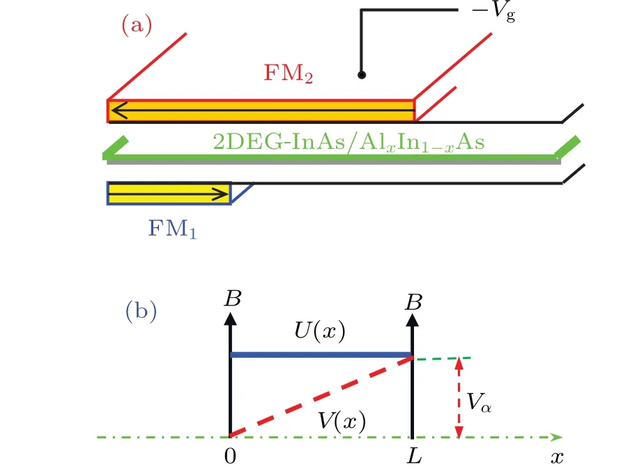
Fig. 1. (a) Schematic diagram of MMSN and (b) magnetic profile and bias voltage.

where the effective potential experienced by electrons in this parallel doubleδ-MB nanostructure can be written as follows:

Evidently, this effective potential is related to not only the magnetic fieldBz(x), wave vectorky, and EBU(x), but also the bias voltageVα. It is difficult to exactly solve Eq. (3)due to the complicated effective potential. Here, we use improved transfer-matrix method (ITMM)[12]to numerically solve Eq. (3). The wave functions of electron can be expressed,in linear combination of plane waves,by
Assuming thatBz(x)andU(x)are constant on theyaxis and change only on thexaxis, the Hamiltonian describing electrons in such an MMSN in the presence of a bias can be given, in a single particle, effective mass approximation, as follows:
wherem*,p,e,m0,andg*are the effective mass,momentum,charge,free mass,and effectiveg-factor of an electron,respectively,µB=e¯h/2m0is the Bohr magneton,andσz=+1/-1


Thus, we can calculate the group delay time and the selfinterference delay time of electron tunneling through this parallel doubleδ-MB nanostructure,respectively,
Using the dwell time, spin polarization of dwell time SP can be characterized by
Here, because time is not an operator in quantum mechanics,how to measure the tunneling time is a controversial problem. So far,the measuring of time is defined in different ways,e.g., the dwell time and the group delay. In this paper,we adopt the dwell time through using plane waves(not wave packets). The temporal separation of the electron spins is usually on the order of 10 ps, which is faster than current operation speed in nanoelectronics and must require advanced techniques to be measured. In our model,the relaxation process is not involved,which deserves to be explored in the future.
3. Results and discussion
In our numerical calculation, the InAs system (g*=15 andm*InAs=0.024m0)is considered as two-dimensional electron gas(2DEG)material,which possesses the basic parametersℓB=81.3 nm,E0=0.48 meV,andτ0=1.39 ps for a typical magnetic fieldB0=0.1T.[8]Thereafter,the partial structural parameters are set to beB=2.0,ky=0.7,andU=9.0,unless otherwise stated. Figure 2(a) shows the dwell time of electrons tunneling through this parallel doubleδ-MB nanostructure, where solid and dashed lines correspond to spin-up and spin-down electrons,respectively. The difference in dwell time between spin-up and spin-down electrons can be observed. Thus,this MMSN still exhibits a significant SP effect when a bias voltage is applied. This phenomenon stems from the spin-field interaction between the electron spin and structural magnetic field. In addition, a peak appears in the dwell time spectrum,that is,the dwell time achieves a maximal value at resonance,where the incident energy of electrons is equal to the binding energy in the MMSN.This spin-dependent dwell time of electrons tunneling through this MMSN indicates that electron spins can be separated in the time dimension,and this finding may be useful for spintronics device applications. Figure 2(b)presents the SP of dwell time as a function of incident energy, where the green and red curves denote the bias voltagesVα=0.0, andVα=2.0, respectively. This figure shows that an evident SP effect in dwell time occurs when electrons tunnel through this nanostructure.Moreover,when a bias voltage is applied to this MMSN,the SP effect of electrons is enhanced,and the SP curve shifts toward the high-energy region.

Fig.2. Curves of(a)dwell time and(b)spin polarization of electron versus incident energy for different parameters.
A controllable spin-polarized source is desired for spintronics device applications.[39]Having known a considerable SP effect in this parallel doubleδ-MB nanostructure when a bias voltage is applied,we next study how such a bias affects the spin-polarized dwell time. First, we apply a positive bias to this parallel doubleδ-MB nanostructure and investigate the effect of positive bias on the spin-polarized dwell time. Figure 3(a)shows the variations of spin-polarized dwell time with incident energy for three bias voltages:Vα=0.0(green curve),2.0 (red curve), and 3.0 (blue curve). Evidently, the SP ratio of dwell time is closely related to the positive bias voltage.When a positive bias is applied to this nanostructure,the spinpolarized dwell time increases,and the SP curve of dwell time shifts slightly toward the high-energy region. The figure also shows that the SP ratio of dwell time is related to the incident energy. To further observe the influence of bias voltage on the SP ratio of dwell time,in Fig.4(b)we directly draw the curves of the spin-polarized dwell timeversusbias voltage for three fixed values of incident energyE=14.0 (green curve), 15.0(red curve), and 16.0 (blue curve). Both magnitude and sign of spin-polarized dwell time greatly change with bias voltage.Moreover, the peak of SP ratio of dwell time increases with bias voltage increasing, and the SP curve shifts rightwards.Clearly, the effect of bias voltage on spin-polarized dwell time results from the dependence ofUeff(E,ky,σz,Vα,x0) onVα. This phenomenon implies that we can control the spinpolarized dwell time by adjusting the bias voltage.
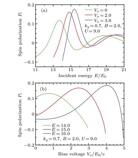
Fig. 3. Curves of spin polarization versus (a) incident energy and (b) bias voltage for different parameters.
Next,we investigate the effect of a negative bias voltage on the spin-polarized dwell time. Figure 4(a) shows the relation between spin-polarized dwell time and the incident energy,where the bias voltage values are fixed atVα=0.0(green curve)-2.0 (red curve), and-3.0 (blue curve), respectively,and the structural parameters are exactly the same as those in Fig.3(a). Evidently,the negative bias voltage also affects the SP of dwell time. However, with the increase of the applied negative bias voltage,the SP of dwell time gradually is weakened, and the SP curve shifts toward the low-energy region.Figure 4(b) shows the influence of negative bias voltage on spin-polarized dwell time. The figure indicates the change of SP of dwell time with negative bias voltage,where the incident energy values are set to beE=14.0 (green curve), 15.0 (red curve), and 16.0 (blue curve), respectively. Figure 4(b) also confirms that the SP ratio of dwell time changes drastically with negative bias voltage. In addition,when the incident energy changes,the SP ratio varies correspondingly. Therefore,spin-polarized dwell time in this parallel doubleδ-MB nanostructure can be controlled by adjusting the negative bias voltage.

Fig. 4. Curves of spin polarization versus (a) incident energy and (b) bias voltage for different parameters.
4. Conclusions
In this work, we investigate the dwell time and the SP of electrons tunneling through a parallel doubleδ-MB nanostructure with a bias voltage, which is constructed by patterning two asymmetric FM stripes on the top and bottom of InAs/AlxIn1-xAs heterostructure,respectively.It is shown that this MMSN still possesses an appreciable SP effect despite a bias voltage is presented inside,which is due to the spin-field interaction between the electron spin and structural magnetic field. It is also shown that both amplitude and sign of the SP can be controlled by appropriately changing the bias voltage,which may lead to an electrically-controllable temporal spin splitter for spintronic device applications.
Acknowledgement
Project supported by the National Natural Science Foundation of China(Grant No.11864009).
杂志排行

Chinese Physics B的其它文章
- Superconductivity in octagraphene
- Soliton molecules and asymmetric solitons of the extended Lax equation via velocity resonance
- Theoretical study of(e,2e)triple differential cross sections of pyrimidine and tetrahydrofurfuryl alcohol molecules using multi-center distorted-wave method
- Protection of entanglement between two V-atoms in a multi-cavity coupling system
- Semi-quantum private comparison protocol of size relation with d-dimensional GHZ states
- Probing the magnetization switching with in-plane magnetic anisotropy through field-modified magnetoresistance measurement