First-principles study on improvement of two-dimensional hole gas concentration and confinement in AlN/GaN superlattices
2022-01-23HuihuiHe何慧卉andShenyuanYang杨身园
Huihui He(何慧卉) and Shenyuan Yang(杨身园)
1State Key Laboratory of Superlattices and Microstructures,Institute of Semiconductors,Chinese Academy of Sciences,Beijing 100083,China
2College of Materials Science and Opto-Electronic Technology,University of Chinese Academy of Sciences,Beijing 100049,China
Keywords: two-dimensional hole gas,III-nitride interfaces,polarization,first-principles calculations
1. Introduction
III-nitrides and their alloys have been widely applied to optoelectronics and transistors.[1,2]Due to their large and tunable direct band gaps ranging from 0.7 eV for InN to 6 eV for AlN, III-nitrides including alloys, nanostructures,and heterostructures have been used in short-wavelength lightemitting diodes,lasers,and high-speed,high-power electronic devices.[3-5]One of the challenges for nitrides is effective ptype doping,especially for GaN and AlN.In these wide band gap semiconductors, p-type dopants tend to be more difficult to ionize,and easier to be compensated by defects.[6]Mg has been considered superior to other p-type dopants because of better solubility, ionization, and compensation in nitrides.[7]However,its ionization energies are still too high(~200 meV in GaN and~600 meV in AlN).[8]Other p-type dopants have even higher ionization energies.[9]Thus,it is difficult to obtain high carrier concentration and mobility in p-doped III-nitrides,severely limiting the applications of III-nitrides.[10]Several approaches have been proposed to overcome this issue, such as Mg-Si co-doping,δ-doping,[11]and pulse doping.[8]Yet these techniques inevitably introduce impurities and suppress the mobility of holes.
An alternative way to obtain high carrier concentration is to make use of the interface charge. Naturally, the most stable structure of III-nitrides is the wurtzite structure with notable spontaneous polarization. At the III-nitrides interface,the large polarization difference will induce interface charge,resulting in two-dimensional electron and hole gases (2DEG and 2DHG).[12]Since the 1990s,many theoretical and experimental research works have been carried out to investigate the 2DEG in III-nitrides heterostructures, and have confirmed a sheet concentration over 1013cm-2.[13]The 2DEG has high mobility since there is hardly dopant-induced scattering at the interface. Various ways such as strain, thickness, alloying,and defects have been widely studied to control the concentration and mobility of 2DEG in III-nitrides,[13-15]and III-nitride based heterostructures have been used to fabricate electronic devices with high performance.[16,17]However,much less effort has been devoted to 2DHG in III-nitride heterostructures.By introducing Mg atoms as dopants in barrier layers,Hsu and Walukiewicz theoretically predicted the formation of 2DHG in AlGaN/GaN heterostructures with a carrier concentration over 1012cm-2.[18]Several experiments proved the existence of 2DHG in GaN-based heterostructures with p-type doped layers.[19-21]In 2019,Chaudhuriet al.firstly observed 2DHG with a high density of about 5×1013cm-2in unintentionally doped GaN quantum wells at AlN/GaN interfaces.[22]Previous theoretical studies on 2DHG are mainly based on onedimensional Schr¨odinger and Poisson equations and unavoidably require empirical parameters, lacking structural details of the interfaces.[23-27]First-principles calculations can predict geometric structures and electronic properties at the IIInitride interface,[28-31]but most of the previous studies rarely discussed how to control the interface charge and distribution.
In this paper, we will study the 2DHG at AlN/GaN interfaces in wurtzite superlattices (SLs) along [0001] direction from first-principles calculations. We will construct various AlN/GaN SLs by changing the in-plane lattice constants and/or the thicknesses of the two constituting materials, and investigate the electronic properties that are closely related to the 2DHG at the interface, including the internal electric fields,band alignments,hole concentrations and distributions. We find that the increasing of in-plane lattice constant could increase the concentration of 2DHG at the interface and slightly enhance the internal fields in both AlN and GaN layers, but would remarkably reduce the valence band offset at the interface. Besides, increasing the thickness of AlN layer and/or decreasing the GaN layer would significantly increase the strength of internal field in GaN layer,improving the confinement of the 2DHG at the interface. Therefore, in order to generate a denser and more localized 2DHG at AlN/GaN interfaces, it is desirable to moderately increase the in-plane lattice constant and increase the thickness ratio between AlN and GaN layers. Our study may provide a guide to control the concentration and confinement of 2DHG at III-nitride interfaces and improve the performance of 2DHG-based devices.
2. Computational methods
We perform first-principles calculations based on the density functional theory(DFT)using the Viennaab initiosimulation package(VASP).[32]We apply the projector augmented wave potentials(PAW)and treat N 2s23p3,Al 3s23p1,and Ga 3d104s24p1states as valence electrons.[33]The plane wave energy cutoff is set as 520 eV.We take the generalized gradient approximation(GGA)of Perdew-Burke-Ernzerhof(PBE)for the exchange-correlation potentials.[34]Γ-centered 8×8×8 Monkhorst-Pack points are used fork-point sampling for wurtzite bulk structures.[35]The atomic coordinates are fully relaxed until the Hellmann-Feynmann forces are less than 0.01 eV/˚A.
To model the interface structures, we constructmAlN/nGaN SLs by connectingmbilayers of AlN andnbilayers of GaN along the [0001] direction (Fig. 1), which is denoted as (m,n) SLs. The space group of the (m,n) SL isP3m1. Thek-point grid for SLs is set as 8×8×kz,wherekzis determined by the lengthcof the SL along the [0001] direction withkz×c~40. Considering the small lattice mismatch between AlN and GaN, we can assume the pseudomorphic growth of the SLs on AlN or GaN substrates, by fixing the in-plane lattice constantato beaAlNoraGaN. To study the strain effect on SLs, we also calculate the free-standing SLs,
whereais relaxed to get the energy minimum of the SLs. In the free-standing SLs, we find thatadepends almost linearly on the concentration of the constitutes and follows Vegard’s law,[36]similar to alloys.
The polarization of the wurtzite bulk nitrides is calculated with the Berry phase method. According to the modern theory of polarization,[37]the formal polarization is calculated by[38]

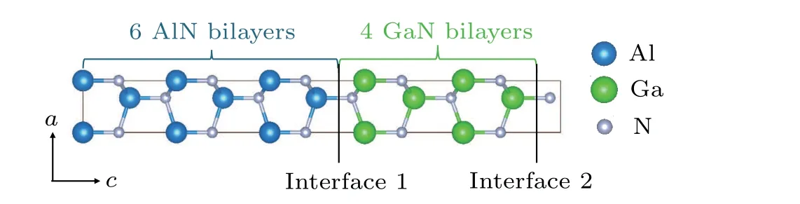
Fig. 1. The structure of mAlN/nGaN SL, which is denoted as (m, n). Here shows the(6, 4)SL.The blue, green, and gray balls denote the Al, Ga, and N atoms,respectively.
3. Results and discussion
The calculated lattice parameters and band gaps for wurtzite AlN and GaN bulk are listed in Table 1. The lattice constants are very close to the previous theoretical values[39]and just slightly larger than the experimental results with an error of less than 1%.[40]The in-plane lattice mismatch between AlN and GaN is calculated to be 2.79%.[42]AlN and GaN are both direct band-gap semiconductors with the valence band maximum (VBM) and conduct band minimum(CBM) located atΓ-point. Table 1 also lists the polarization parameters of wurtzite AlN and GaN. By taking H-phase as the reference structure, the spontaneous polarizationsPspof wurtzite AlN and GaN are calculated to be 1.326 C/m2and 1.305 C/m2,respectively,in excellent agreement with the previous calculations.[39]The piezoelectric constante33should be the same whether choosing H-phase or zincblende structure as the reference.[39]Here, our calculatede33in GaN is smaller than that in Ref. [39], but is in better agreement with other calculation results.[43]

Table 1. The lattice parameters, direct band gaps, spontaneous polarizations, and piezoelectric constants in wurtzite AlN and GaN bulk.H-phase is chosen to be the reference for the polarization parameters.
3.1. Interface hole concentration
Firstly, we would like to clarify the origin of the interface charge in AlN/GaN SLs. III-nitrides are known for their remarkable polarizations. And there exists a large polarization difference between AlN and GaN.This large polarization discontinuity would lead to the bound of charges at AlN/GaN interfaces. We use the interface theorem to get the bound polarization charge at the interface in SLs:[37]if the interface is insulating and dislocation-free, the interface bound charge density can be determined by the difference of the formal polarization,i.e.,

Two types of interfaces can be formed in AlN/GaN SLs,as denoted by interfaces 1 and 2 in Fig.1. At interface 1,the polarization of AlN on the left is always smaller than that of GaN on the right, resulting in a positive bound charge at this interface. In other words, the 2DHG would be formed at interface 1. Similarly,there will be 2DEG at interface 2. In this paper,we mainly focus on the 2DHG at interface 1.
To study the strain effects on the interface charge, different in-plane lattice constantaof (m,n) SLs have been considered:aAlN,aGaN, andafor free-standing SLs. In the free-standing SL,atakes some value betweenaAlNandaGaNdepending on the numbersmandn. Following the previous studies,[38]the formal polarizations of AlN and GaN in the SLs are calculated from their bulk structures by using the Berry phase method,with the same in-plane lattice constantaas that in the SLs. Then the interface hole charge density at interface 1 can be obtained from Eq. (2), as shown by open squares in Fig.2. The formal polarization of strained wurtzite structure has two contributions: the formal polarization of an unstrained wurtzite structure and the strain induced piezoelectric polarization. By using H-phase as the reference, the formal polarization of a strained wurtzite structure can be calculated as

whereeijdenotes the piezoelectric constants, andεis the strain, i.e.,ε3= (c-c0)/c0andε1=ε2= (a-a0)/a0.[45]Equation (3) indicates that the piezoelectric effect is also of importance to the difference of polarization at the interface.The calculated interface charges density using Eqs.(2)and(3)are shown by the solid squares in Fig.2,which are consistent with the data calculated from the Berry phase method.
As seen from Fig.2,the 2DHG at the AlN/GaN interface has a high concentration with a magnitude of 1013cm-2. Besides, the hole concentration varies linearly with the increase of the in-plane lattice constanta. Whenais fixed to the AlN bulk valueaAlN, the hole concentration is 5.0×1013cm-2.Since we use the formal polarizations at zero electric field in Eq. (2), the calculated interface charge corresponds to SLs with infinite thickness, which is the limit of a single heterostructure.[38]Thus,the value is in good agreement with the experimental result for a single AlN/GaN heterostructure in Ref. [22]. This indicates that the estimation of the interface charge from bulk polarization is satisfactory, although the structural distortion near the interface has been ignored.Asais increased toaGaN, the charge density increases to 7.1×1013cm-2.concentration of 2DHG in AlN/GaN heterostructures can be obtained by increasing the in-plane lattice constant. Besides the concentration, we also need to consider the spatial distribution of the interface holes, which is closely related to the internal field and the band offset as discussed below.

Fig.2. The charge density of 2DHG at AlN/GaN interface 1 as a function of in-plane constant a. Open and solid squares indicate data calculated directly from Berry phase method(referred to H-phase)and from Eq.(3),respectively.
3.2. Internal field
The bound charges at the interfaces induce internal fields within the SLs. With positive charges at interface 1 and negative charges at interface 2,the internal fields in GaN and AlN layers are in opposite directions. The internal fields result in a change in the potential as well as in the atomic core-levels,and we can determine the internal field from the slope of N-1s core levels in the SLs.[31]Figure 3(a)shows the N-1s core level shifts in(8,8)SLs(i.e.,8AlN/8GaN),where the thicknesses of both AlN and GaN layers are comparable to each other. With the in-plane lattice constantavarying fromaAlNtoaGaN, the strength of the internal field in AlN increases from 5.0 MV/cm to 5.6 MV/cm,and that in GaN increases from 4.5 MV/cm to 4.9 MV/cm. In other SLs withm=n=4, 6, 10, the internal fields in both AlN layer and GaN layers are also increased by around 0.50 MV/cm with increasinga. These results are consistent with Ref. [30], where the strength of the internal electric field in GaN is slightly changed from 4.7 MV/cm to 5.4 MV/cm asaincreases fromaAlNtoaGaN,regardless of the layer thickness. For(m,n)SLs withm/=n,the in-plane lattice constantaalso has a small influence on the internal fields. For example, in(4, 22)and(22, 4)SLs with very different thicknesses of AlN and GaN layers, the changes of internal field are always less than 1 MV/cm by varying the in-plane lattice constants. Therefore,the strain effect on the internal fields in AlN/GaN SLs is quite limited.
On the other hand,the thickness of the AlN or GaN layer strongly influences the internal electric fields. Here we take the free-standing SLs as an example. As shown in Fig. 3(b),when the number of GaN layersnchanges from 4 to 8 in(8,n)SLs, the internal field in GaN decreases from 6.0 MV/cm to 4.5 MV/cm,while that in AlN layer increases from 3.4 MV/cm to 5.1 MV/cm. When the number of AlN layersmchanging from 4 to 8 in(m, 8)SLs, the strength of the internal field in GaN increases from 3.0 MV/cm to 4.5 MV/cm, whereas that in AlN layer decreases from 7.0 MV/cm to 5.1 MV/cm, as shown in Fig. 3(c). It seems that a thicker AlN layer and/or thinner GaN layer will result in a stronger internal field in GaN layer and a weaker internal field in AlN layer. To further check the thickness effect,we consider two free-standing SLs, one with thick AlN layer and the other with thick GaN layer. In (4, 22) SL with a very thick GaN layer, the internal field in AlN reaches up to 9.1 MV/cm, larger than those in other SLs with thinner GaN layer. And the electric field in GaN is much weaker, only 1.4 MV/cm. On the other hand,in (22, 4) SL with a very thick AlN layer, the internal field in GaN (7.5 MV/cm) becomes much larger than that in AlN layer (1.6 MV/cm). Herein, the increase of the thickness of AlN layer leads to a noticeable enhancement of the field in GaN layer by several times.
In order to quantitatively understand the influence of strain and thickness on the internal field, we turn to an electrostatic model. Following Ref.[46],we take the short-circuit boundary condition for AlN/GaN SLs,i.e.,the potential drop throughout the whole period of SL is zero. The electric field in GaN can then be expressed as[47]

whereLAlNandLGaNare the lengths of the AlN and GaN layers, respectively, andεAlNandεGaNare their respective dielectric constants. The internal field in AlN layer has a similar expression. The variation in the in-plane lattice constantacan induce a moderate change in the interface charge density as discussed in Subsection 3.1. Therefore, the change ofacan not significantly influence the internal field. However, the thickness of AlN and/or GaN layers can lead to a more remarkable change in the internal field. A smaller ratio ofLGaN/LAlNcorresponds to a larger field in GaN and a smaller field in AlN. The ratio of the internal fields satisfies-EAlN/EGaN=LGaN/LAlN. In Fig. 3(d), we plot the ratio of internal fields as a function of the ratio of the lengths in AlN/GaN SLs, where we find an excellent linear relationship between them.
Note that the electric fields in a single AlN/GaN heterostructure are different from those in the SLs due to the different boundary conditions.[46]Since the polarization is influenced by the internal fields, the interface bound charges in these short-period SLs are smaller than that in a single heterostructure.[38]By using the experimental dielectric constants,[47]the hole concentration at interface 1 in (8, 8)SL witha=aAlNis calculated to be 4.7×1013cm-2from Eq. (4), slightly smaller than the value of 5.0×1013cm-2obtained in Subsection 3.1. At a larger in-plane lattice constanta=aGaN,the calculated hole concentration in(8,8)SL is 5.2×1013cm-2, much smaller than 7.1×1013cm-2obtained in Subsection 3.1 due to the larger internal fields in this SL.
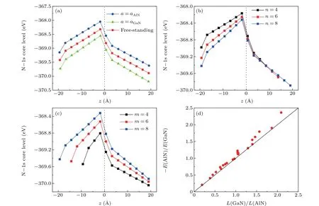
Fig.3. N-1s core level profiles in(a)(8,8)SLs under different strains,(b)(8,n)free-standing SLs with n=4,6,and 8,and(c)(m,8)free-standing SLs with m=4,6,and 8. Here z=0 indicates the position of the interface 1. (d)The ratio of the internal fields between AlN and GaN as a function of their length ratio in different AlN/GaN SLs.
3.3. Hole distribution
The internal field in GaN layer induces a slop in the potential, forming a triangle quantum well that confines the 2DHG near the interface.To investigate the influence of the internal field on the hole distributions in SLs,we introduce holes in the system by removing 0.01 electron per supercell and sum over all the empty valence band states.[46]This charge removal corresponds to a density of hole around 1013cm-2. Figure 4 shows the hole distributions in free-standing(4,8)and(22,8)SLs. We can see that the 2DHG is mainly confined in the GaN layer and is very close to interface 1.This is in good agreement with experimental results,where the holes are confined within a few atomic layers in GaN near the interface(~1 nm).[19]In comparison, the distribution of 2DEG at interface 2 is more delocalized over a few nanometers.[48]This is one of the advantages of 2DHG in III-nitride heterostructures. As shown in Fig. 4(a), the peak of hole distribution in (4, 8) SL is around the second GaN bilayer near the interface,whereas the peak in(22, 8)SL appears around the first GaN bilayer. Besides, the hole distributes over 7 GaN bilayers in (4, 8) SL, but it only distributes over 5 bilayers in (22, 8) SL. This indicates that holes in free-standing (22, 8) SL are more localized within GaN layer than those in (4, 8) SL. This can be attributed to the larger internal field in GaN layer in (22, 8) SL due to the thicker AlN layer. Besides, decreasing the thickness of GaN layer would also increase the internal field in GaN and enhance the localization of holes. For instance, in free-standing(8, 4)and(8,8)SLs,the peaks of hole distribution appear at the first and second GaN bilayers near the interface, respectively(not shown).
Previous studies also proved the thickness effect on the hole confinements. Nakajimaet al.discovered that the 2DHG density is larger in heterostructures with a thicker AlGaN barrier.[49]Yanet al.confirmed better hole confinement and a higher hole density in systems with thicker AlGaN layers based on one-dimensional simulations.[27]Therefore,we conclude that a thicker AlN barrier layer and/or a thinner GaN layer(i.e.,a smaller ratio ofLGaN/LAlN)results in better confinement of 2DHG at the AlN/GaN interface by inducing a stronger internal field in the GaN layer.

Fig.4. The distribution of 2DHG in free-standing(a)(4,8)and(b)(22,8)SLs. The upper panels show the partial charge densities with isosurface value of 5×10⁻⁶ Bohr-3. The below panels show the plane-averaged hole densities along the SL direction. Blue and green dash-lines indicate N positions in AlN and GaN layer,respectively,and gray lines denote the position of the interfaces.
3.4. Valence band offset
The band offset at the interface is one of the most important physical quantities in a heterostructure. In AlN/GaN heterostructures, the valence band offset (VBO) determines the depth of the quantum well that confines the 2DHG at interface 1,as shown in Fig.5(a). And a larger VBO ensures better confinement of holes in the quantum well. Here, we take the N-1s core levels as the reference energies to calculate the band offsets at the AlN/GaN interface.[31]The procedure is schematically shown in Fig. 5(a). Firstly, the N-1s core levels throughout the AlN/GaN SLs are calculated as in Subsection 3.2. Next,the relative positions of band edges of AlN and GaN with respect to the N-1s core levels are obtained from the strained bulk calculations. Then we align the band edges of AlN and GaN in the SLs using the N-1s core levels as the energy references.
The calculated VBOs as a function of the in-plane lattice constantafor various AlN/GaN SLs are shown in Fig. 5(b).We can see that the lattice constantahas an essential effect on the VBO. For pseudomorphic AlN/GaN SLs with a fixed value ofa,the VBO is almost independent of the thicknesses of the two materials. Whenais fixed toa=aAlN,VBO at the AlN/GaN interface is around 0.71 eV,regardless of the thickness of the two materials(see the blue dots in Fig.5(b)). This result is in excellent agreement with the experimental value of 0.70±0.24 eV from x-ray photoemission spectroscopy for the pseudomorphic GaN layer on AlN substrate.[50]However,whenais fixed toa=aGaN,VBO at the interface is decreased to around 0.28 eV.Therefore,a=aAlNis preferred toa=aGaNin pseudomorphic SLs in order to maintain a large VBO and to avoid the leak of currents,although the interface hole concentration is smaller,as discussed in Subsection 3.1.
For free-standing AlN/GaN SLs where the in-plane lattice constantais between those of AlN and GaN bulk values,the VBO values decrease almost linearly with the increase ofa, as shown in Fig. 5(b). It is possible to choose a suitableain free-standing SLs for a better balance among the interface hole concentration,distribution,and the VBO at the AlN/GaN interface. Since the hole concentration at differentais large enough and the hole confinement is good enough,it is more effective to improve the VBO by changinga. A larger thickness ratio ofLGaN/LAlNresults in a largeraand thus larger hole concentration at the interface, but probably with a smaller VBO. For free-standing (4, 8) SL, the hole concentration is 6.4×1013cm-2,and the VBO is calculated to be 0.43 eV,still large enough for the confinement of 2DHG at the interface.

Fig. 5. (a) Schematic diagram of band edge profile of AlN/GaN SLs along z direction. (b) VBOs as a function of in-plane lattice a in (m, n) SLs. At a=aAlN and a=aGaN, the data correspond to(22, 4), (8, 4), (7, 5), (8, 8),(6,8),(4,8),and(4,22)SLs from the bottom to up.
But too largeawould degrade VBO too much. On the other hand,a smaller ratio ofLGaN/LAlNresults in a smallera,corresponding to a smaller hole concentration but better confinement and larger VBO. In a free-standing (8, 4) SL where the thickness of AlN layer is about twice of GaN layer,the VBO at the interface is as high as 0.57 eV,and the hole concentration reaches 5.9×1013cm-2with good confinement near the interface.
The influence of the in-plane lattice constant on the VBO at the AlN/GaN interface can be understood by the strain effect on band gap. In AlN/GaN SLs, AlN is under tensile biaxial strain,while GaN is under compressed biaxial strain. Asaincreases fromaAlNtoaGaN,our calculations show that the band gap of bulk AlN decreases from 4.05 eV to 3.48 eV. The decreasing of the band gap leads to an upshift of VBM for AlN.Meanwhile,the band gap of GaN is found to be only slightly decreased from 1.82 eV to 1.71 eV,resulting in a much smaller upshift of GaN VBM state than that of AlN. Therefore, the VBO at the AlN/GaN interface decreases with increasinga.
4. Conclusion
In this work, we perform first-principles calculations to systematically investigate how to control the concentration and confinement of the polarization-induced 2DHG at interfaces in AlN/GaN SLs by changing the in-plane lattice constantaand the thicknesses of each constituent. The 2DHG concentration at AlN/GaN interfaces calculated from polarization discontinuity is consistent with the experimental results, and can be increased from 5×1013cm-2to 7×1013cm-2by increasingafromaAlNtoaGaN. However, this would decrease VBO at the interface from 0.72 eV to 0.28 eV, which might lead to a leakage problem at largea. We also find that an increase in the ratio of AlN to GaN thicknesses would significantly enhance the internal electric field in GaN,improving the hole confinement near the interface. In pseudomorphic SLs,a=aAlNis preferred toa=aGaNdue to a better VBO. In free-standing SLs, it is possible to choose a suitableafor a better balance among the interface hole concentration, distribution, and the VBO. A larger ratio of AlN to GaN thicknesses results in a smallera,leading to better hole confinement and larger VBO,but slightly smaller hole concentration, and vice versa. Our study could serve as a guide to improve the hole concentration and/or the confinement of the 2DHG at the III-nitride interfaces,which would help to optimize the performance of relevant devices.
Acknowledgments
Project supported by the National Key Research and Development Program of China (Grant No. 2018YFB2202801)and the National Natural Science Foundation of China(Grant No.12074369).The calculations were performed on TianHe-2 at National Supercomputer Center in Lv Liang of China.
杂志排行

Chinese Physics B的其它文章
- Superconductivity in octagraphene
- Soliton molecules and asymmetric solitons of the extended Lax equation via velocity resonance
- Theoretical study of(e,2e)triple differential cross sections of pyrimidine and tetrahydrofurfuryl alcohol molecules using multi-center distorted-wave method
- Protection of entanglement between two V-atoms in a multi-cavity coupling system
- Semi-quantum private comparison protocol of size relation with d-dimensional GHZ states
- Probing the magnetization switching with in-plane magnetic anisotropy through field-modified magnetoresistance measurement