First-principles study of structural and opto-electronic characteristics of ultra-thin amorphous carbon films
2022-01-23XiaoYanLiu刘晓艳LeiWang王磊andYiTong童祎
Xiao-Yan Liu(刘晓艳), Lei Wang(王磊), and Yi Tong(童祎)
College of Electronic and Optical Engineering&College of Microelectronics,Nanjing University of Posts and Telecommunications,Nanjing 210023,China
Keywords: amorphous carbon,density,optical properties,electronic structure,density functional theory
1. Introduction
Amorphous carbon (a-C) films possess three types of bonding hybridizations: sp3, sp2, and sp1.[1]Tailoring the sp3/sp2hybridization ratios causes a-C to exhibit various crystalline and amorphous structures when changing from diamond(sp3)to graphite(sp2). Therefore,a-C with a relatively high sp3/sp2ratio is termed as diamond-like carbon (DLC).Owing to its high mechanical hardness, chemical inertness,and low thermal conductivity,DLC has been used in applications such as protective coatings for storage disks,optical windows, and electroluminescent films.[2-4]Furthermore, these advantages, which are associated with a low surface work function,enable the use of a-C in flat panel displays and photoelectric emitter devices.[5,6]Additionally, by adjusting the sp3/sp2hybridization ratio, the electronic properties of a-C films can be rapidly and reversibly switched between a high resistive state (HRS) and a low resistive state (LRS). As a result, a-C is a promising medium for non-volatile memory applications.[7,8]A majority of the aforementioned applications, particularly the electronic and optical applications, require ultra-thin films. It is, therefore, important to determine the opto-electronic properties of ultra-thin a-C films (which have thicknesses≤5 nm).
However, the opto-electronic properties of ultra-thin a-C films,such as the refractive index and electrical resistivity,are yet to be investigated experimentally,which is likely due to the technical difficulties involved in measuring the physical properties of ultra-thin films. As a result, considerable attention has recently been devoted toward computationally predicting the physical/chemical characteristics of a-C media by using the density functional theory (DFT). Davilaet al.calculated the density of states (DOS), degree of electronic states’ localization, and transmission function for bulk a-C using the DFT.[9]Deringeret al.used machine learning and DFT calculations to study the surface chemistry of tetrahedral a-C(ta-C)and estimate the surface energy of the amorphous form of this material.[10]Galliet al.[11]and Mathioudakiset al.[12]calculated the electronic properties of 54 carbon atoms and the mechanical properties of 216 atomic amorphous carbon networks by using first-principles calculations. Liuet al.investigated the electronic and optical effects of bulk a-C with different sp3/sp2hybridization ratios.[13]In most of the aforementioned studies, bulk a-C materials were examined. A detailed physical analysis of ultra-thin films has not been reported thus far.In addition,a previous study reported that temperature has a significant impact on the physical characteristics of amorphous materials;[14]thus,it may also influence the opto-electronic properties of a-C materials,which has not been investigated in previous studies. To address these issues and accurately determine the material characteristics, we present a sophisticated theoretical framework for modeling ultra-thin a-C films by using the DFT.The structural,electronic,and optical properties of a-C films featuring thicknesses of 1 nm and 5 nm(i.e., the two extreme cases of“ultra-thin”)were calculated under temperatures from 100 K to 900 K and were then analyzed in detail.
2. Methods
Structural optimization was performed by using the wellknown Viennaab-initiosimulation package (VASP).[15,16]VASP was also used to conduct theab-initiomolecular dynamic (AIMD) calculations for a-C materials with different thicknesses, in order to determine their optimized structures under various temperatures. The cutoff energy was set to be 400 eV, and the Perdew-Burke-Ernzerhof (PBE) functional with the generalized gradient approximation was used to describe the electronic properties of a-C materials.[17,18]The projector augmented wave was also used to describe the coreelectron interactions.[19,20]The force threshold was set to be 0.05 eV/˚A, and the energy threshold was set to be 10-4eV.Slabs with thicknesses of 1 nm and 5 nm were built,and their differences were analyzed. To generate the amorphous carbon structure,we imported a certain number of carbon atoms into the slabs at random positions,and the number of carbon atoms was determined based on the density of the carbon slab. In this study, five different densities that covered the range of possible values reported in literature were considered:[13,21]1.52, 1.99, 2.47, 3.03, and 3.51 g/cm3. To construct carbon slabs with different densities, the number of carbon atoms for a given density was first calculated according to the volume and mass of the carbon atoms. The calculated carbon atoms were subsequently imported into the system, and the force field calculations were performed at 900 K for 1 ns in order to relax the structures. The resulting structures were then employed in the following AIMD calculations. In this case, the coordinate number of carbon atoms were counted to determine their hybridization states. The 1 nm structure contained 19, 25, 31, 38, and 44 carbon atoms corresponding to the five aforementioned densities, respectively. Thek-points were set to be 1×1×1, following the Monkhorst-Pack scheme.[22]These structures first underwent relaxation at high temperatures(8000 K)and were then annealed to 100,300,500,700,and 900 K.OpenMX,which combines the DFT with non-equilibrium Green’s function calculations,was used to calculate the electric resistivity.[23-26]The C PBE19 functional and s2p2d1orbital basis were used in this case. The cutoff energy was set to be 150 Ry (2.04 keV), considering the higher cutoff energy required due to the orbital mixing. As a result, the energy threshold was set to be 10-5Hartree (2.7×10⁻⁴eV).[27]As the electronic structure and opto-electronic properties of ultra-thin a-C films have not been reported in detail thus far, we calculated the volume fraction of sp3bonding inside the bulk a-C as a function of the sample densities and subsequently compared the values with the corresponding experimental measurements.[21]For the aforementioned calculations, all bulk a-C structures were firstly subjected to structural relaxations at high temperatures(8000 K)and subsequently annealed to 300 K. Thereafter, the coordinate numbers of each atom in the resulting structures were calculated. sp3bonding was defined as one particular carbon atom being connected with three neighboring atoms. In this study, the interatomic distance was set as 1.75 ˚A. This value was not chosen arbitrarily,and most C-C bond distances were~1.45 ˚A.[28]A variety of interatomic distances were tested during our simulations,and interatomic distances ranging from 1.5 ˚A to 2.0 ˚A afforded the same coordinate numbers for all the carbon atoms. Thus,the statistical results of all the sp3bonds inside the structures with different densities were obtained,as shown in Fig.1. The calculated sp3volume fractions were slightly lower than the corresponding experimental values.Nevertheless,bulk a-C with a higher density featured a larger volume fraction for sp3bonding,which was highly similar to the experimental observations. In addition,the slope fitted for the calculation results was found to be 70.1(g/cm3)-1,which was in good agreement with the slope fitted for the experimental results(70.2(g/cm3)-1). This confirms the physical validity of our calculation model.
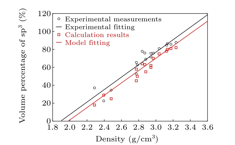
Fig. 1. Calculated and experimentally measured volume fractions of sp3 bonding as a function of the bulk a-C densities.
3. Results and discussion
The bonding in the 1-nm and 5-nm a-C films under the five aforementioned densities is schematically shown in Figs.2(a)and 2(b),respectively. Figure 2(a)shows that the 1-nm a-C structure with the lowest density contains sp/sp2/sp3bonded C atoms. Structures with a higher density have a smaller proportion of sp-bonds in the a-C structure, and the denser structures examined here only contain sp2and sp3bonded atoms. However, the sp3/sp2hybridization ratio is higher when the density exceeds 3 g/cm3. As the density of the pure sp2-bonded graphite and sp3-bonded diamond were reported to be 2.24 g/cm3and 3.54 g/cm3,[29]respectively, it is reasonable to infer that the 1-nm-thick a-C film with a density<2.5 g/cm3features an adequately large space to be filled with C atoms, thus leading to an abundance of sp2bonded atoms. When the density exceeds 3 g/cm3, the interatomic forces between the atoms are sufficiently strong to form a sp3-like structure. The extent of sp2/sp3hybridization in the 5-nm-thick a-C film (see Fig. 2(b)) is analogous to that in the 1-nm-thick structure. Most of the 5-nm-thick structure is occupied by sp2hybridized atoms when the density is lower than 2.5 g/cm3, whereas the film with a density of 3.03 g/cm3has approximately equal fractions of sp2and sp3atoms. The volume fraction of the sp3-bonded atoms begins to exceed the fraction of sp2-bonded atoms only when the density is at least 3.51 g/cm3. A comparison with the 1-nm structure shows that an a-C structure with an increased thickness is likely to provide more space for atomic oscillations,whereby the sp3bond becomes the dominant component when the density is relatively high.

Fig.2.Examples of the a-C films structures with densities of 1.52,1.99,2.47,3.03,and 3.51 g/cm3,respectively(from left to right)for(a)1-nm thickness and(b)5-nm thickness.
The volume fractions of the sp2-and sp3-bonded C atoms in the 1-and 5-nm-thick a-C films were also calculated at the temperatures ranging from 100 K to 900 K, and the results are shown in Fig.3. The volume fraction of sp3bonds in the 1-nm film at room temperature (300 K) gradually increases from 4% to 81.8% as the density increases from 1.52 g/cm3to 3.51 g/cm3(Fig.3(a));these results agree with the observations from Fig.2. In addition to the above mentioned dimension, we also investigated the influence of the cross-sectional size on the resulting sp2/sp3volume fractions. This was exemplified by using a 1-nm slab with a cross-section four times larger than that of its counterpart,as shown in Fig.2,at a density of 3.51 g/cm3(i.e., 176 atoms). Despite this significant difference in dimension, the calculated sp2/sp3volume fractions only changed by~3%. Additionally,the upper limit of the total number of atoms that VASP can process,in the case of small high-performance computer clusters,is~200;[30]thus,it is highly computationally expensive to further enlarge the cross-section. It is,therefore,believed that the original dimensions described in Fig. 2 afford a sufficiently high physical accuracy,without sacrificing computational efficiency.
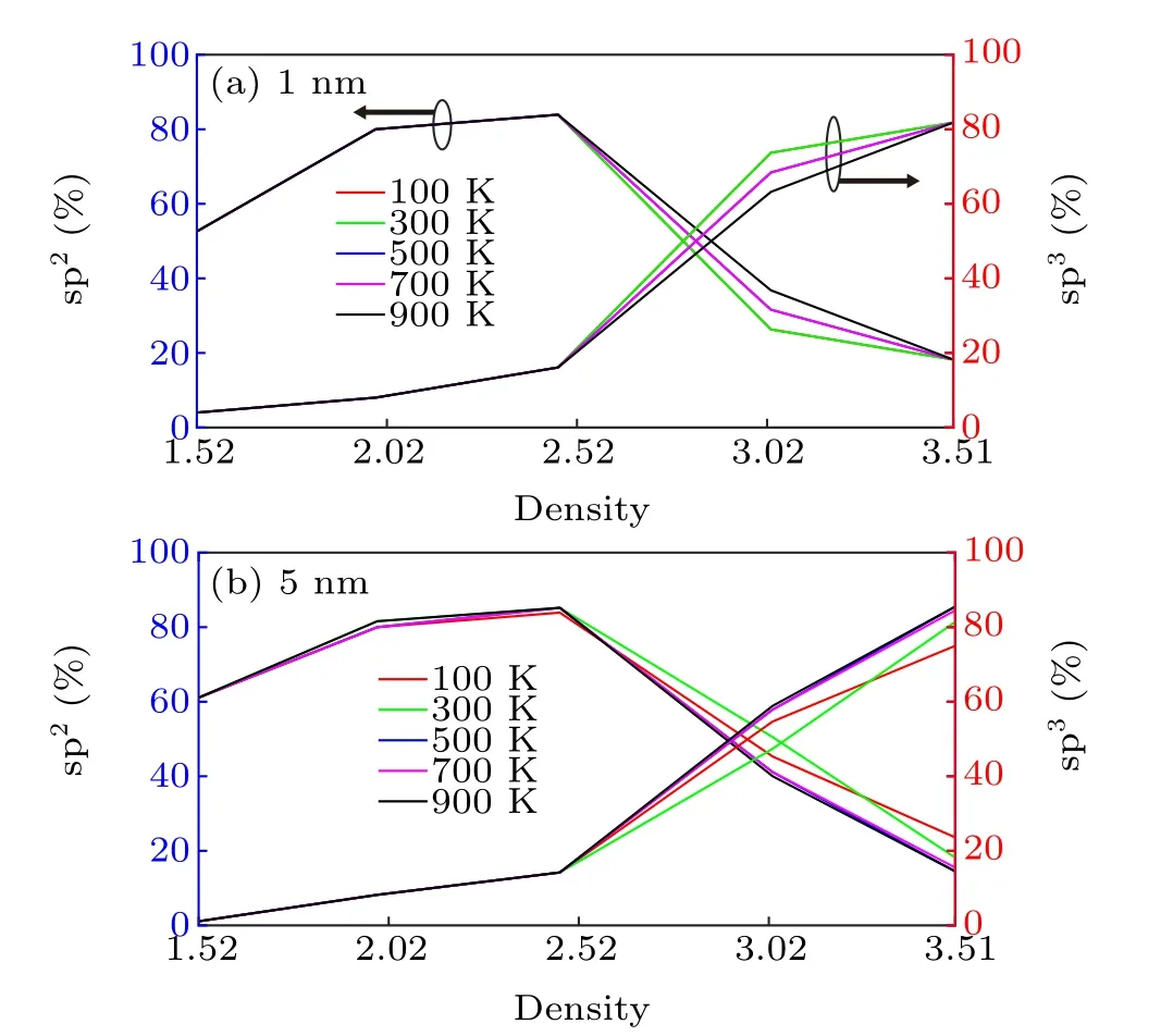
Fig. 3. Volume fraction of sp2 and sp3 bonded C atoms as a function of the temperature varying from 100 K to 900 K and density changing from 1.52 g/cm3 to 3.51 g/cm3 for(a)1-nm-thick a-C film and(b)5-nm-thick a-C film,respectively.
It should also be noted that the proportion of sp2-bonded C initially increases with the density increases and reaches a maximum value (~83.9%) at a density of 2.47 g/cm3, and a-C films with higher densities have lower proportions of sp2-bonded C.It is possible to infer that,under low densities,the available space is large with respect to the carbon atoms, implying that carbon atoms can be coordinated with each other more easily. To maintain the carbon structure with a relatively stable configuration, sp2hybridization may be favorable. However, the cases with densities≥2.52 g/cm3imply that the carbon structure tends to be closely packed. With considering that the carbon atoms with sp3hybridization have the greatest extent of space utilization,the amount of sp3-bonded C is expected to increase in order to maximize the extent of space utilization and stabilize the system. The above mentioned density-dependent trend is also reflected in the 5-nm film(Fig.3(b)). The sp3-bonded fraction increases from 1.1%to 85.5%at room temperature as the density increases. Meanwhile, the sp2volume fraction reduces to less than~85.2%when the density exceeds 2.47 g/cm3. In general, a-C with higher densities contains greater s-p hybridization. This is expected because a certain system always tends to possess a structure that minimizes its energy. Specifically, sp2bonds have higher energy than sp3bonds due to the larger s orbitals in sp2hybridization and the shorter interatomic distances between adjacent carbon atoms. This implies that the overall system is more likely to contain more sp2orbitals as this will cause the structure to have a lower internal energy. This speculation is valid for relatively low densities(below 2.5 g/cm3).However, when the density increases up to 3 g/cm3, the system has less space for all the sp2-hybridized carbon atoms,and some of the a-C atoms transform from sp2to sp3to enhance space utilization. Furthermore,figure 3 shows that the proportion of sp2/sp3does not change with temperature. This is because the range of investigated temperatures is below the melting temperature of a-C materials (~4000 K),[31]and the lattice vibrations and thermal motions are too weak to affect the general coordination of a-C atoms in a-C structures with different densities of a-C.As a result,although the exact atomic positions differ with temperature,varying the temperature for a particular a-C structure only has a weak influence on the consequent proportion of sp2/sp3(at least within the range investigated in this study).

Fig.4. Band structure at 900 K as a function of different densities for a-C thickness of(a)1 nm and(b)5 nm.
The band structures of the 1-and 5-nm-thick a-C films at five different densities and 900 K are depicted in Figs.4(a)and 4(b), respectively. Although band structures typically apply to periodic crystal systems, the investigated amorphous carbon films also exhibit limited periodic structures at the tens of angstroms scale.[32]Consequently, the band structures calculated here may potentially reveal the microscopic-scale electronic structure of a-C thin films. Figure 4(a)shows that using a 1-nm-thick a-C film at a relatively low density results in a small energy gap near the Fermi level. In this study, as the structures with high densities contain more atoms and form more bands, the formed bands overlap and thus decrease the band gaps. For the 5-nm-thick structure, no evident bandgap was noted at densities lower than 3.03 g/cm3. The a-C structure with a density of 3.51 g/cm3has a wider gap between 0.5 eV to 2 eV. This is expected because the structure with a density of 3.51 g/cm3may be similar to the structure of diamond, as both structures have the same high density. Under such densities, most of the carbon atoms are sp3hybridized,and no excess electrons can be provided for delocalization.This implies that the electrons face difficulties in traveling between the valance band and the conduct band,which possibly explains the 0.5 eV-2 eV band gap. The band structure of the ultra-thin a-C films appears to be independent of temperature,and this is likely due to the superior thermal stability of a-C films,which is not illustrated here.
The total density of states (TDOS) for the 1- and 5-nmthick a-C films at 900 K is shown in Figs. 5(a) and 5(b), respectively. These results are generally consistent with the calculated band structures, which are depicted in Figs. 4(a) and 4(b),respectively.As seen in Fig.5(a),the TDOS value is nonzero at the energy range of-5 eV to 5 eV for the 1-nm-thick a-C films at 900 K,and no evident energy band gaps are noted.This is consistent with the results shown in Fig.4(a).For the 5-nm-thick a-C films at 900 K,only the structure with a density of 3.51 g/cm3exhibits small gaps, as shown in Fig.5(b),and this also matches the structure with a density of 3.51 g/cm3,as shown in Fig. 4(b). These bandgaps only exist in certain limited structures,a representative of which is the 5-nm-thick structure with a density of 3.51 g/cm3. This phenomenon suggests that electrons in the valence band can still be excited to the conduction band,provided the structure is significantly thin. As a result, sp2electrons in a-C structures with lower densities can be more easily transferred throughout the material. In addition,most energy bands in the 5-nm structure are found to be mutually crossed when the density ranges from 1.99 g/cm3to 3.03 g/cm3,and there are no band gaps in these structures. This clearly demonstrates that some of the a-C atoms in these structures still possess the ability to transport additional electrons. This observation is significant and helps obtain electronic information regarding a-C materials. Under a particular density, the band structures of the ultra-thin a-C films are found to be independent of their temperature environment,owing to the aforementioned reasons.

Fig.5. Total density of state(TDOS)at 900 K as a function of different densities for a-C thickness of(a)1 nm and(b)5 nm.
Interestingly, as shown in Fig. 5, the calculated TDOS shows significant fluctuations under the aforementioned five densities. Such a trend was also observed for the amorphous carbon films with larger cross-sections(i.e.,176 atoms),which indicates that it is independent of the model dimensions. Another possible reason for these fluctuations may be the chosen computational parameters (e.g., ‘SIGMA’) governing the TDOS. A larger SIGMA can, in principle, reduce the TDOS fluctuations. To assess the impact of SIGMA on the calculated TDOS, SIGMA was artificially increased to an un-realistic value of 0.2 eV, which is four times higher than the default setting of 0.05 eV for both insulators and semiconductors.Despite these variations, relatively large fluctuations were still noted, which implies that computational parameters may not be the main factor causing the fluctuations. According to the above mentioned discussions, the strong fluctuations of the TDOS near the Fermi level can be ascribed to the intrinsic complexity of the amorphous carbon system,which results in complex electronic states near the Fermi level.
We subsequently calculated the optical properties of the 1-and 5-nm-thick a-C structures at different temperatures and densities. The temperature-dependent complex refractive index of the 1-nm a-C films with a density of 3.51 g/cm3and the corresponding density-dependent refractive indexes at 900 K are shown in Figs.6(a)-6(d). The complex refractive index is directly derived from the complex dielectric constant,which is obtained using the DFT/MD calculations,and expressed as[33]
whereωis the frequency,nandkare the real and imaginary parts of the refractive index, respectively, andε1andε2are the real and imaginary parts of the complex dielectric constants of the a-C films, respectively, which are obtained from the aforementioned DFT/MD models. In Eq. (1),nindicates the phase velocity, andkrefers to the extinction coefficient,which quantitatively indicates the amount of attenuation when an electromagnetic wave propagates through a material. According to Figs. 6(a) and 6(b), for the 1- and 5-nm-thick a-C films with a density of 3.51 g/cm3,nis lower when the photon energy is higher, particularly when the energy<1 eV. The value ofnremains constant once the energy exceeds 5 eV.Temperature has a slight impact on the resulting value ofnfor all the densities considered in this study. Figures 6(c)and 6(d) also show that, for a given temperature, the 1-nm-thick a-C films with densities below 3 g/cm3exhibit several peaks from 1 eV to 5 eV. The values of such peaks range from 1 to 3. However, in the 5-nm structure, the presence of a wide peak is witnessed, whennis approximately 2 for the structures with densities of 3.03 g/cm3and 3.51 g/cm3. This is because it is more difficult for the photons to pass through a material with higher density. At a density of 3.51 g/cm3, the value ofkundergoes a continuous reduction as the energy increases, for the 1-nm film; by contrast, the value ofkfor the 5-nm film initially increases along with the energy, reaches a maximum value at~12.5 eV, and then decreases rapidly.Varying the temperature has a slight impact on the resultingk. Unlike its temperature independence,the value ofkfor the ultra-thin a-C films was found to be strongly dependent on the film densities,as indicated in Figs.6(c)and 6(d). At a low energy level (≤5 eV), 1-nm films with higher densities exhibit higher values ofk. This trend continues until the energy exceeds 15 eV,after which the value ofkfor the 1-nm films was found to be insensitive to the densities. For the 5-nm films,the structure with the lowest density exhibits the largest value ofk, which gradually decreases on increasing the density, especially at an energy below 5 eV.Further increasing the energy weakens the variations inkunder the different densities, andkappears to be independent of the energy beyond 20 eV. As density reflects the extent of sp2/sp3hybridization,the extinction coefficient of the sp2-dominated a-C thin film differs from that of its sp3-dominant counterpart, particularly in the longwave regime. As a result,switching the volume fraction of sp2or sp3bonding can significantly alter the refractive index and consequently the transmittances of ultra-thin a-C films. This may enable the application of these films in optical storage media for emerging photonic memories in the near infrared(NIR)region.[34-36]
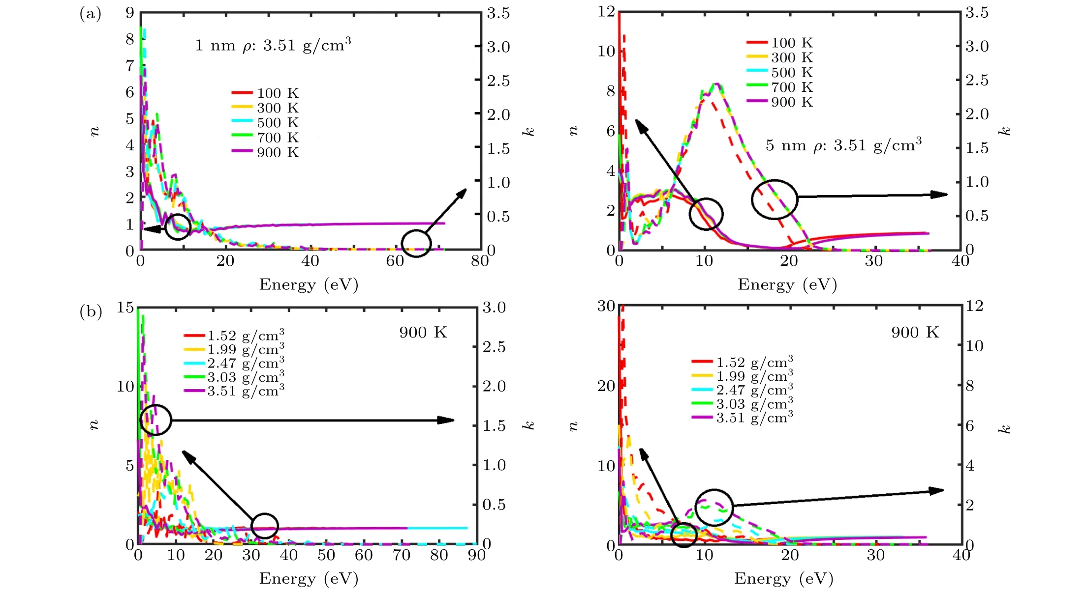
Fig.6. Calculated refractive index(a)at density of 3.51 g/cm3 as a function of different temperatures from 100 K to 900 K for a-C thicknesses of 1 nm (left) and 5 nm (right), and (b) at temperature of 900 K as a function of different densities from 1.52 g/cm3 to 3.51 g/cm3 for a-C thickness of 1 nm(left)and 5 nm(right).
The temperature and density-dependent absorption coefficients of the 1-nm and 5-nm a-C films were calculated and plotted, as shown in Figs. 7(a) and 7(b), respectively. As shown in Fig.7(a),the 1-nm film with a density of 3.51 g/cm3has an absorption coefficient that initially increases with the photon energy and reaches a maximum value of 1×106cm-1near 7 eV (~177 nm). A similar trend was also observed for the 5-nm a-C film, whose maximum absorption coefficient was found to be 3×106cm-1at~12 eV. The absorption coefficient spectra were dependent on the intrinsic properties of the material,such as the hybridization and the shortrange and long-range order associated with surface relaxation.All these parameters may influence the absorption coefficient values. With considering that such parameters vary significantly between the 1-nm and 5-nm a-C structures, it is reasonable for the 1-nm and 5-nm configurations to exhibit two different maximum absorption coefficients at different energies. Figure 7(a) also shows that temperature plays a minor role in determining the absorption coefficient of the 1-nm a-C films. The 5-nm-thick a-C film with the greatest sp3proportion (i.e., 3.51 g/cm3) exhibits a lower absorption coefficient at 100 K than at higher temperatures, particularly when the photon energy exceeds 10 eV.The density-dependent absorption coefficient of the 1-nm a-C films is uniform across the investigated portion of the optical spectrum, as illustrated in Fig. 7(b). However, the a-C films with relatively low densities (e.g.,<3.03 g/cm3) exhibit several small peaks in the absorption coefficient from 4 eV to 15 eV, whereas the a-C films with a density≥3.03 g/cm3usually exhibit only one large wide peak in the same energy band. In contrast to the 1-nm film,the 5-nm-thick a-C film with a low density exhibits peaks from 3 eV to 8 eV and 10 eV to 15 eV.Nevertheless,the peak from 3 eV and 8 eV is lower and the peak from 10 eV and 15 eV is higher when the density is higher. As high absorption coefficients correspond to a greater quantum efficiency,a-C films with higher densities(i.e.,greater sp3contents)produce greater attenuation and less transmittance. These results can be understood because a-C structures with higher densities have more sp3C atoms and produce a smaller mean free path for the photons owing to their close-packed structures.In addition,the sp3-hybridized structures are also non-planar,and no spare electrons can be shared to conduct photocurrents,which suggests that the photoconductivity of these films is lower. To compare the values of the absorption coefficient peaks for the 1-nm and 5-nm films, it is reasonable to assume that the absorption coefficients of the 5-nm structures are usually two times higher than those of the 1-nm film,under the same conditions.

Fig. 7. Calculated absorption coefficients (a) at density of 3.51 g/cm3 as a function of different temperatures from 100 K to 900 K for a-C thicknesses of 1 nm(left)and 5 nm(right),and(b)at temperature of 900 K as a function of different densities from 1.52 g/cm3 to 3.51 g/cm3 for a-C thickness of 1 nm(left)and 5 nm(right).
In addition to the absorption coefficients,the dependence of the reflectivity of the a-C films on temperature and density was calculated, and the results are shown in Figs. 8(a)and 8(b). Figure 8(a) shows that the reflectivity of the 1-nm a-C film with a density of 3.51 g/cm3is relatively high at longer wavelengths and decreases with the wavelength. The dependence of reflectivity on the temperature remains negligible. This agrees with the previous finding that the 1-nm a-C film has low and high absorption coefficients at low and high energy levels, respectively. In the 5-nm a-C film, reflectivity decreases on increasing the energy up to 1 eV, after which it gradually increases along with the energy and begins to decrease again beyond 20 eV.Up to an energy of 20 eV,the reflectivity of the 5-nm a-C film remains almost constant under different temperatures,and on further extending the energy beyond 20 eV,reflectivity is nearly independent of temperature.Figure 8(b) shows that the reflectivity with a value of 0-0.5 exhibits several peaks (ranging from 0 to 0.5) from 0 eV to 15 eV in the case of the 1-nm structures with densities of 1.52,1.99, and 2.47 g/cm3. However, structures with higher densities do not appear to exhibit such peaks,and the reflectivity gradually decreases as energy increases. The 5-nm structures with densities exceeding 1.5 g/cm3exhibit a wide peak from 10 eV to 20 eV, whereas the 1-nm structures mainly reflect light at lower energies. In summary,denser and thicker structures possess greater reflectance. It should also be noted that the 5-nm structures with high densities(>2.5 g/cm3)tend to have a low reflectance at lower energies.
Figures 9(a)and 9(b)show the energy loss functions for the 1-nm and 5-nm structures with a density of 3.51 g/cm3under different temperatures and for a temperature of 900 K at different densities, respectively. The energy loss peaks in the 1-nm structure are distributed uniformly across the overall energy spectrum,whereas only one energy loss peak is observed for the 5-nm structure. The effect of temperature on the resulting energy loss in the 1-nm a-C film is negligible, as shown in Fig. 9(a). However, the peak position of the 5-nm structure at 100 K is located at a lower energy,as compared to that at other temperatures. Regarding the density-dependent energy loss(Fig.9(b)),the peaks in the energy loss functions for the 1-nm films are distributed over the entire energy spectrum.Nevertheless,the 5-nm-thick structure shows peaks at a more positive energy position when the density is higher, allowing for similar peak shapes. This indicates that the 5-nm a-C film has a more ordered structure,and an atomic configuration similar to that of diamond is ensured at a density of 3.51 g/cm3.On increasing the density, the a-C structures exhibit higher peak values. This suggests that, for the 5-nm structures, the remaining energy after the incident light passes through the a-C films gradually decreases as the density is increased. This is consistent with the high absorption coefficients of these structures,as shown in Fig.7.
In addition to the optical properties of the ultra-thin a-C films, we evaluated the electrical resistivity of the ultra-thin a-C films by varying their density and temperature. These results have not been previously reported, to the best of the authors’knowledge. The electrical resistivity of the 1-nm and 5-nm a-C films as a function of density and temperature is illustrated in Figs. 10(a) and 10(b), respectively. Generally,the 1-nm-thick a-C structure has a resistivity of~1011Ω·m.This is consistent with the amorphous structure, where electrons cannot be readily delocalized and transported; hence,a-C materials can be considered as insulators in the absence of external stimuli. Under the same thickness, a-C structures with densities exceeding 3 g/cm3have slightly lower electrical resistivities than the films with lower densities. As a highdensity structure comprises more sp3carbon atoms, a small number of electrons can undergo transport via longer mean free paths. Compared with the 1-nm-thick structures, the 5-nm-thick a-C structures exhibit analogous electrical resistivity,which appears to contradict the previous finding that a-C films with thicknesses greater than 10 nm typically have lower electrical resistivities as the thickness increases.[37]It should be noted that the a-C thicknesses considered in this study are significantly less than 10 nm and thus exhibit a more pronounced quantum confinement effect, resulting in electrical behaviors different from those observed for greater thicknesses (e.g.,≥10 nm). This causes discrepant thickness-dependent resistivity between the ultra-thin and thicker films. Temperature has a weak influence on the resulting electrical resistivity of the 5-nm a-C films, and the 5-nm structure with a density of 3.51 g/cm3tends to have higher resistivity than the films with the remaining four densities. This is in good agreement with the aforementioned results for the band structures and the DOS. For instance, the 5-nm film with a density of 3.51 g/cm3has an average resistivity of 2.8×10¹¹Ω·m,which corresponds to a large bandgap obstructing electron transfer.Moreover, the energy loss function shown in Fig. 9 also implies that the high-density structures usually exhibit the largest peaks at higher energies. Therefore, it is reasonable to infer that the higher peak positions and values of the energy loss function may be correlated with a significant transition of the electrons from the valence band to the conduction band;thus, structures with higher densities would have higher resistivities. The electrical resistivity of a fairly thick a-C film(>10 nm)switches between the HRS(sp3bonding)and LRS(sp2bonding) under Joule heating, but this does not seem to apply to the ultra-thin a-C films (<5 nm) considered in this study;[38]thus, extremely low electrical resistivities are independent of the bonding structures. As a result, ultra-thin a-C films may not be considered as an appropriate candidate for non-volatile storage media. It should also be noted that the physical mechanism governing the aforementioned resistance switching in thick a-C films still remains unclear. However,because the electrical resistivity of ultra-thin a-C films with sp3/sp2-bonding was found to be independent of temperature,it is reasonable to ascribe such electrical switching behavior to an electrically induced effect, which warrants further investigation.

Fig. 9. Calculated energy loss function (a) at density of 3.51 g/cm3 as a function of different temperatures from 100 K to 900 K for a-C thicknesses of 1 nm(left)and 5 nm(right),and(b)at temperature of 900 K as a function of different densities from 1.52 g/cm3 to 3.51 g/cm3 for a-C thickness of 1 nm(left)and 5 nm(right).

Fig. 10. Calculated electrical resistivities with respect to different temperatures and densities for a-C film thickness of(a)1 nm and(b)5 nm.
4. Conclusion
In this study, a theoretical framework was developed to elucidate the electronic structure and opto-electronic characteristics of ultra-thin a-C films at different densities (ranging from 1.52 g/cm3to 3.51 g/cm3) and temperatures (ranging from 100 K to 900 K) based on the DFT. It was found that temperature plays a minor role in determining the electronic structure and opto-electronic characteristics of ultra-thin a-C films,whereas density was found to have a significant impact.The simulation showed that the volume fraction of sp3bonding increases with density, whereas that of sp2bonding initially increases, reaches a maximum value at 2.52 g/cm3, and then decreases rapidly. The 1-nm-thin film exhibited a pronounced band gap;however,this band gap was not observed for the 5-nm structures with low densities.The extinction coefficients of the ultra-thin a-C films were also found to be density-sensitive in the long-wavelength regime. This implies that switching the volume ratio of sp2to sp3bonding can effectively alter the transmittances of ultra-thin a-C films, which could serve as a novel approach toward photonic memory applications. Nevertheless,the electrical resistivity of ultra-thin a-C films appears to be independent of temperature. This implicitly indicates that the electrical switching behavior of a-C films previously utilized for non-volatile storage applications is likely due to an electrically induced effect and not a purely thermal consequence.
Acknowledgments
ProjectsupportedbytheNUPTSF(Grant Nos. NY220078, NY217116, and NY220112), the Science Foundation of Jiangsu Province, China (Grant Nos. BK20211273 and BZ2021031), the Dual Innovative Doctor of Jiangsu Province, China (Grant No. JSSCBS20210522), the Institution of Jiangsu Province, China(Grant No. 20KJB510014), the National and Local Joint Engineering Laboratory of RF and Micro-assembly (Grant No. KFJJ20200203), the Industry Program of Huzhou City(Grant No. 2020GG03), the Distinguished Professor Grant of Jiangsu Province, China (Grant No. RK106STP18003),the Jiangsu Province Research Foundation, China (Grant Nos. NLXZYZZ219001 and SZDG2020009), the National Natural Science Foundation of China (Grant No. 61964012),and the Foundation of Jiangxi Science and Technology Department,China(Grant No.20202ACBL212001).
猜你喜欢
杂志排行

Chinese Physics B的其它文章
- Superconductivity in octagraphene
- Soliton molecules and asymmetric solitons of the extended Lax equation via velocity resonance
- Theoretical study of(e,2e)triple differential cross sections of pyrimidine and tetrahydrofurfuryl alcohol molecules using multi-center distorted-wave method
- Protection of entanglement between two V-atoms in a multi-cavity coupling system
- Semi-quantum private comparison protocol of size relation with d-dimensional GHZ states
- Probing the magnetization switching with in-plane magnetic anisotropy through field-modified magnetoresistance measurement