Fabrication of Josephson parameter amplifier and its application in squeezing vacuum fluctuations∗
2021-12-22PengtaoSong宋鹏涛XueyiGuo郭学仪KaiXu许凯XiaohuiSong宋小会ZhanWang王战ZhongchengXiang相忠诚HekangLi李贺康LuhongSu苏鹭红YirongJin金贻荣andDongningZheng郑东宁
Pengtao Song(宋鹏涛) Xueyi Guo(郭学仪) Kai Xu(许凯) Xiaohui Song(宋小会) Zhan Wang(王战)Zhongcheng Xiang(相忠诚) Hekang Li(李贺康) Luhong Su(苏鹭红)Yirong Jin(金贻荣) and Dongning Zheng(郑东宁)
1Beijing National Laboratory for Condensed Matter Physics,Institute of Physics,Chinese Academy of Sciences,Beijing 100190,China
2School of Physical Sciences,University of Chinese Academy of Sciences,Beijing 100049,China
3Songshan Lake Materials Laboratory,Dongguan 523808,China
Keywords: Josephson parameter amplifier,squeezed state,quantum computing
1. Introduction
It has been well known that Josephson parameter amplifier(JPA)has very low noise level for microwave signals.[1]In recent years,it has attracted renewed interests since it is a suitable pre-amplifier for performing single-shot superconducting qubit readout.[4]With the use of a JPA, experimental observations of quantum jumps[5]and quantum feedback control of qubit states have been reported.[6]Even more,JPAs are being used in ultra-sensitive dark matter detection experiments.[7]In the simplest form, a JPA has a relatively narrow amplification bandwidth in the order of 10 MHz that is unsuitable for frequency multiplexed readout scheme of superconducting qubit devices and other applications.[8,11]To realize broadband JPA,a number of different methods have been proposed and realized.[9,10,26]Previously,broad bandwidth JPA devices using the design in Ref. [9] have been made by using fabrication process involving wet etching of Al films,[11]and the devices are used in a number of quantum experiments. In this work,we fabricate JPAs by using a modified process that combines structures made of Nb films and Josephson junctions of aluminum. This process can reduce and simplify fabrication steps. The device we fabricated with this process exhibits a 15 dB gain value and amplification bandwidth about 400 MHz with near- quantum limit noise performance. We also use this device to demonstrate the squeezing of vacuum fluctuations,achieving about 1.635 dB-squeezing of the power spectral density.
2. Fabrication procedure
The schematic circuit of the broadband JPA is shown in Fig.1(a)that is similar to the design reported in Ref.[9]. The key parts of the circuit are a non-linear LC resonator and a tapered impedance transformer. The resonator is formed by a superconducting quantum interference device (SQUID) loop and a capacitor. The amplification is realized by driving the resonator into non-linear region. This is achieved by applying a pump signal whose frequency is about twice of the input signal. The impedance transformer increases the coupling strength between the JPA and the environment and,hence,decreasesQfactor to achieve broadband amplification.[9]
In our device,the critical current of SQUID is 4µA(2µA for each Josephson junction)and the capacitance is 5.5 pF.The center frequency is around 7.4 GHz. The impedance transformation is realized by covering the parallel plate capacitor cross-overs on the signal CPW transmission line.[9,12]
The fabrication process uses e-beam lithography in every step, with a large current 50 nA for coarse structures and a small current of 100 pA for fine structures,in order to reduce the total exposure time.
The first step of fabrication is deposition of Nb film on high-resistance(greater than 10 kΩ)silicon substrates. Before deposition,the substrates are cleaned by using the mixture of ammonium hydroxide and hydrogen peroxide(1:1 in volume)to remove organic substances and then using 10%hydrofluoric acid to remove the silicon dioxide layer whose dielectric loss is very high. The growth of Nb film is performed by magnetron sputtering in an ultra-high vacuum chamber.
In the second step, we pattern the niobium film with reactive ion etching with a mixture of Ar and SF6, after defining the coarse structures using EBL.The e-beam photoresist is ZEP520A(ZEON).What we need to pay attention in this step is that the plasmas can etch substrate and the etching rate of silicon is very fast. Thus,if the etching time is too short,some areas on the film are etched completely and others are not because of the non-uniformity of film thickness. If the etching time is too long,the substrate will be over-etched. This could,on the one hand, change the impedance of the transmission line and, on the other hand, make the subsequent preparation of Josephson junctions more difficult. Our experience shows the best over-etch depth of substrate is about 50 nm to 100 nm.
The third step involves deposition of a dielectric layer and subsequent etching for the plate capacitor and crossovers of impedance transformer. The resist we used is ZEP520A.The dielectric material is amorphous silicon which is grown with plasma enhanced chemical vapor deposition (PECVD)method. Then we etch the silicon with plasmas generated by HBr. The advantage of choosing HBr is it does not etch niobium.
In the next step, we grow aluminum film with electron beam evaporation, and then lift-off the film above the photoresist(ZEP520A+PMGI), to form the top electrode of the capacitor and crossovers. It is important to note that the thickness of the aluminum film must be thicker than silicon film,otherwise the connection will be broken.
In the final step, we fabricate Josephson junctions with Dolan bridge shadow evaporation technique.[12,27]An double layer resist (PMMA950/MAA8.5) design is used for making the bridge. We evaporate the first aluminum film obliquely,and then put oxygen into the chamber to generate a very thin AlOxlayer,followed by evaporating the second aluminum film vertically to form Al/AlOx/Al junctions.
We chose niobium instead of aluminum as the first layer for the following reasons.Compared to the aluminum film,the niobium film can be easily distinguished from the substrate under a small current scanning electron microscope because the atomic number of niobium and silicon is largely different.Thus, it is not necessary to make Au marks for EBL alignment. The physical strength of the niobium film is high and the chemical propertied are stable,which can improve the device yield.

Fig.1. Experiment setup. (a)Circuit diagram of the JPA.A JPA consists of a plate capacitor and a SQUID,which couples to the environment strongly by an impedance transformer. In the left port,a circulator is used to separate the reflected signal. In the right port,a direct current and a microwave pump signal are used to tune the critical current of SQUID and to provide power,respectively.(b)Experiment setup for homodyne measurements.The output signals are amplified by a HEMT mounted at 4 K stage and a room temperature amplifier,respectively,and then sent to the RF port of an IQ mixer with a local frequency fpump/2. The quadrature signals I and Q are digitized by two analogue-digital converters(ADC)and then processed by a field programmable gate array(FPGA)in real time.
2.1. Characterization of device performance
Characterization of the broadband JPA device is carried out by using a vector network analyzer. The device is placed inside a dilution refrigerator that provides a 15 mK base temperature.The JPA is worked in a reflection mode.A very weak signal(∼−120 dBm to−140 dBm)is input,amplified and reflected back. A circulator is used to separate the input and reflected output signals.The output signal is further amplified by a commercial high-electron-mobility transistor (HEMT) amplifier(LN-LNC48C Low Noise Factory),mounted at the 4 K stage of the dilution refrigerator,and a room temperature amplifier. There is an isolator between HEMT and JPA to block the noise of the HEMT. The pump signal emitted by a microwave source and the DC signal generated by a DC source are coupled through a bias-tee to another port of the JPA.
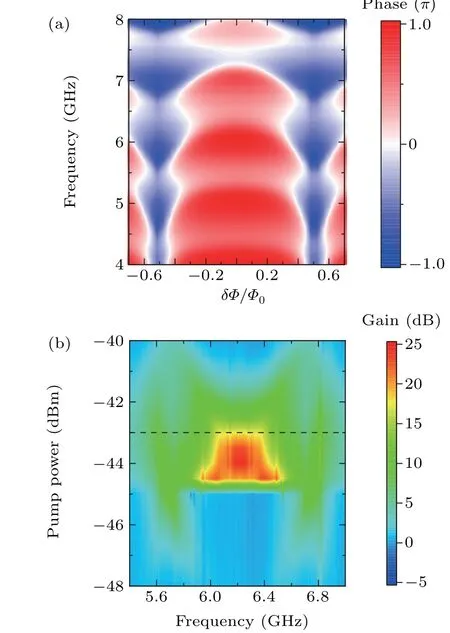
Fig. 2. Tuning and gain. (a) The phase component of measured S21 parameter as a function of DC bias for different input signal frequency. It shows the frequency of JPA tuned by external magnetic field. (b)Gain of JPA measured at different DC bias values and pump amplitudes for a fixed pump frequency 12.5087 GHz. The gain is defined by |S21on|/|S21off|,where|S21on|and|S21off|are the amplitudes of S21 parameter with pump on and off,respectively.
In the following section,we describe procedures for tuning a JPA.We can tune the inductance of SQUID via the DC bias current which can generate flux through the loop.It means the resonant frequency of JPA can be tuned accordingly. We measureS21parameter as a function of DC bias and observe periodical variation as shown in Fig.2(a). The data presented in the figure areS21phase component data measured between 4–8 GHz for different biases. Some variation along the frequency axis is observed,that is attributed to parasitic modes.
The amplification frequency range depends on the bias,pump frequency and amplitude. In principle, one may adjust bias to change the amplification frequency range. However,after many measurements,we find that the device exhibits better performance when it is biased in the flat region near zero or integer flux quantum. We normally measure gain as a function of input signal frequency and pump amplitude.In Fig.2(b),we plot measured data for a fixed pump frequency 12.5087 GHz.The input signal is set at−110 dBm. This 2D gain spectrum graph shows the amplification frequency region. By changing the pump frequency, we get many 2D spectra which provide clues to the working range of the device. Furthermore, the data we get show that we might tune bias slightly to obtain improved gain. The data in Fig. 2(b) show there is a region(the red color region)over which gain can exceed 20 dB.But we shall show later, the noise performance is poor in this region.
A good amplifier shows not only high gain value and broad bandwidth, but also low noise temperature. Generally speaking, it is difficult to obtain low noise temperature and gain-bandwidth performance at the same time. So, we need to balance these two factors according to experiment requirement.
Noise temperature is an important indicator to judge whether a JPA is practically useable. An advantage of JPA is its near-quantum-limited noise performance. To estimate the noise temperature of JPA,we assume that the output signal power measured with turning on and off JPA can be expressed as[13]

whereTpandGpare the noise temperature and the gain of the JPA,THandGHare the noise temperature and the gain of the HEMT,Tcand Gcare the noise temperature and the gain of room temperature amplifier,Giis the insertion loss of the circulator,Gais the attenuation of the line,Tsysis the system noise temperature, andσis the standard deviation of the signal.
According to the three formulas above, we can get the noise temperature of JPA By assuming the vacuum noise at 15 mK is small, we may ignore the system noiseTsys,and get

In our system,we already know
therefore, we need only to measure the standard deviation of the signal by turning on and turning off JPA to getσonandσoff, respectively. In practice, we obtainσonandσoffby taking 2000 times measurements for a given signal. The spread data points follow the Gaussian distribution. After this, the noise temperature of the devices is calculated.
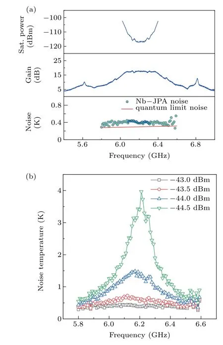
Fig.3. Performance. (a)Frequency dependence of the saturation power,gain and noise temperature. The data were taken at a working point with pump power of −43 dBm. The saturation power is defined as the 1 dB compression point. The quantum limit noise is defined as the equivalent temperature of one photo energy. (b) The noise temperature versus frequency curves measured at different pump powers.
We have measured noise temperature at different pump amplitude. The results are presented in Fig. 3(b). Clearly,noise temperature varies significantly with pump amplitude.We find at pump power of−43 dBm the noise temperature is about 0.4 K that is close to the quantum limit. In Fig. 3(a),we show noise temperature data measured at−43 dBm together with saturation power and gain data. There is about a 15 dB flat gain, a 400 MHz amplification bandwidth, a saturation power greater than−120 dBm and a near-quantumlimited noise performance.
At some other pump powers,we can get a flat 20 dB gain and a 500 MHz bandwidth, but the noise temperature is also very high. After a number of systematic measurements, we conclude that the region shows the highest gain value does not normally show good noise performance. We normally reduce gain slightly by changing pump power and can find an optimized working point. The open black square symbols in Fig.3(b)correspond to a good working point of pump power.
We also find that, by adjusting the pump frequency, the device can work from 4 GHz to 7.5 GHz, but gain-frequency profiles can be quite different,which are greatly influenced by the external admittance.[9]
3. Qubit readout
For superconducting qubits, dispersive measurement is most commonly used qubit readout scheme.[22–24]When a qubit is coupled with a cavity in the dispersive regime,the cavity frequency depends on the qubit state. In dispersive measurement, there are only a few photons stored in the cavity,so the probe signal power is very weak. Using JPA as a preamplifier can improve signal to noise ratio(SNR)significantly.
The JPAs we fabricated have been applied to multi-qubit readout in a number of experiments. Data shown in Fig.4 represents one example.The performance of the gain and amplification bandwidth is shown in Fig.4(a). The readout resonator signals are usually demodulated into in-phase(I)and quadrature (Q) components. In Fig. 4(b), we show the data in theI–Qplane. The red and blue dots represent data points taken for qubits prepared at|0〉and|1〉states, respectively. In this case, we repeat the measurement for 3000 times for|0〉state and 3000 times for|1〉state. Clearly,when the JPA is on,the separation of the two data point clouds representing the quantum states|0〉and|1〉is larger. The large separation allows faster readout and improved measurement fidelity.
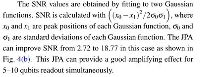

Fig.4. Qubit readout. (a)Measured response of S21 of a superconducting Xmon qubit device with the JPA pump power on and off,respectively. The lower panel shows the gain value obtained from the data of the upper panel. Clearly,the amplification bandwidth around 200 MHz is achieved with the gain more than 15 dB.The dips in S21 curve are readout resonator modes. (b)Upper panels: The readout resonator signal data shown in the I–Q plane. The blue and red dots represent|0〉and|1〉states of qubit,respectively. The data have been rotated to make the line through both centers of two clouds to be parallel to I-axis. Lower panels: Distribution of data points along the I-axis.
4. Realizing squeezed state
In quantum mechanics, the variances of a pair of conjugate variables are limited by the Heisenberg uncertainty principle. It has been suggested that one may generate squeezed states, in which the variance of one variable can be deceased while the variance of another variable is increased, to ensure that the product of two variances is still limited by the Heisenberg uncertainty principle.
The theory of squeezed state of light was firstly introduced in the 1960s,[14–16]and became matured in the 1980s.[17]In 1985, Slusheret al.observed squeezed state generated by four-wave mixing at optical frequency.[18]Then in 1986, Wuet al.also realized squeezed state by threewave mixing at optical frequency.[19]Similarly, people have generated squeezed states at microwave frequency using JPAs.[2,3,20]In this work,we investigate squeezing of vacuum state generated by a JPA with three-wave mixing.
The theory that using parametric amplifier to realize squeezed state is described by Wallset al.in 1984.[25]The interaction Hamiltonian of non-degenerate parametric amplifier is given by[17,25]
wherea1,a2, andbare the annihilation operator of signal,idler and pump modes,respectively,andκis the coupling constant. When the pump mode power is large,boperator can be replaced as a classical field asεe−iωpt,whereωpis pump frequency.
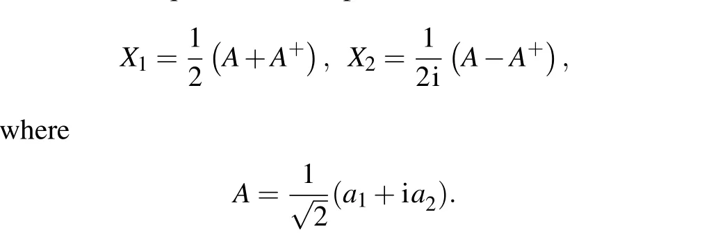
Then the quadrature components are defined as
The variance ofX1andX2areV(X1) = (1/4)e2randV(X1)=(1/4)e−2r, respectively, wherer=κεt, andtis the interaction time.
The homodyne setup used to detect squeezed state is shown in Fig. 1(b). The equivalent temperature of vacuum fluctuation at 6 GHz is about 144 mK (i.e., a half photon energy) while the environment temperature is about 15 mK.Thus,it is reasonable to assume that the input signal is mainly due to the vacuum fluctuations when there is no microwave signal input.
The output signals are amplified by the HEMT and room temperature amplifiers, respectively, before being transmitted to the RF port of anIQmixer that operates with a local frequencyfpump/2. The quadrature signalsIandQare digitized by two analogue-digital converters(DACs)and then processed by a field programmable gate array (FPGA) in real time. The output of the JPA consists of modes at signal frequency (fpump/2)+δand idle frequency (fpump/2)−δ. TheIQmixer down-converts the two modes to the same intermediate frequencyδ.We calculate the complex amplitudes(i.e.,IandQcomponents)of these two modes,respectively,and then add them together.Because these are quantum correlations between the two modes,the resulted data can show squeezing in some directions in theI–Qplane which is equivalent toX1–X2plane. This means the squeezing will be observed in theI–Qplane.
We can define the difference of power spectral densities∆Swith JPA on and off as measured squeezing level. Thus,
withSon=Gs(ςon+kBTn)andSoff=Gs(ςoff+kBTn).
Here,SonandSoffare the power spectral densities with JPA on and off.Gsis the total gain of amplifier chain,Tnis the equivalent noise temperature of the detection chain when JPA is off,kBis Boltzmann constant,ςonandςoffis the original signal with JPA on and off.
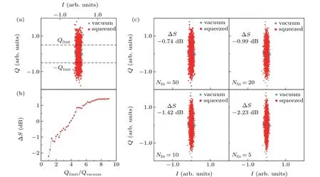
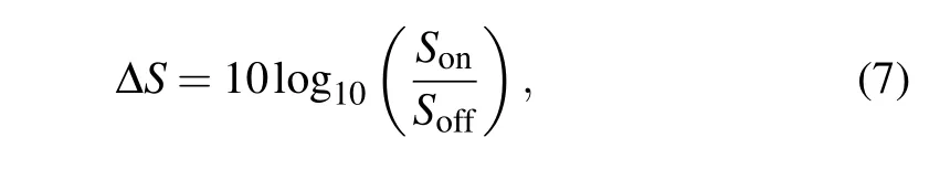
Fig.5. Illustration of vacuum fluctuations squeezing by the JPA.(a)The circular distributed blue dots are the IQ data measured with JPA off. The dumbbell distributed red dots are the IQ data measured with JPA on. The data are taken with δ =50 MHz. The two dashed lines define the region in which data are used for calculation of ∆S using Eq.(7)(see text). (b)Dependence of ∆S on Qlimit/Qvacuum,where Qvacuum is the maximum Q value of the vacuum state. (c)The data after phase noise correction with different Nfit values. The smaller the Nfit is, the more the squeezed data points distribution shape is like an ellipse. The ∆S value is calculated using Eq.(7).
To obtainSonandSoff, we first project the data to theIaxis and then fit the projected data using a Gaussian function.The power spectra density is the square of the standard derivation of the Gaussian function.
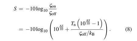
After that,we can get the actual squeezing levelSby[3,20]
When the input state is vacuum state,ςoff=(1/2)ħω0,whereω0is the signal frequency.
Once we obtain the measured squeezing level ∆SandTn,we can calculate the actual squeezing levelS. It means an observed squeezed state when ∆Sis below zero.
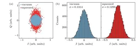
Fig.6. Effect of squeezing with low phase noise. (a)Vacuum state(blue dots)and squeezed state(red dots),which are measured with two channels of the same microwave source. (b)The statistics of the number of points along the I axis in Fig.6(a). We fit the histograms with Gaussian functions.Here σ is the standard derivation of Gaussian function and is used for the calculation of the measured squeezing level ∆S using Eq.(7).
The results of squeezing vacuum fluctuations withδ=50 MHz are shown in Fig.5(a), where vacuum and squeezed states are represented by 2000 blue and red points, respectively. The squeezed direction in theI–Qplane is determined by the relative phase between pump and local microwave sources, and we have adjusted the squeezed direction to theI-axis.
We note that the data point distribution of squeezed state shows a dumbbell shape rather than an expected ellipse shape.We suggest this is caused by the phase noise between pump and local microwave sources.
The phase noise leads to a small and random rotation of squeezed state around the original point in theI–Qplane, resulting in the dumbbell shape. Nevertheless, the squeezing along theI-direction is clear in the figure. To obtain ∆Squantitatively,we choose part of the squeezed data between−QlimitandQlimitto calculate ∆Sand find that ifQlimitis small enough∆Swill become smaller than zero,indicating squeezing of vacuum fluctuations. The relation between ∆SandQlimitis shown in Fig.5(b).
Furthermore,by assuming the relative phase between the microwave sources is stable during a short period of time,we may correct the phase noise manually. We fit every sequentially measuredNfitdata points to a line by minimizing the total distance between each point to the line,and then align all fitted lines to obtain the corrected data distribution, as shown in Fig.5(c). We find that the smaller theNfitis, the more the squeezed data points distribution like an ellipse. The ∆Svalue for data after phase noise corrections is calculated. Apparently, the measured squeezing level of 2.23 dB value may be obtained.
To confirm the problem of phase noise, we measure the phase noise with different brands of microwave sources. We find that the phase noise level of two microwave sources with same clock source is better than the microwave sources with different clock source. Then we use the same clock sources,and check the phase noise. The worst results are measured on two microwave sources with different brands (the test instruments are Keysight-PSG E8257D and Sinolink-SLFD-D).The better results are obtained with two same brand microwave sources (Keysight-PSG E8257D). The best results are measured with two channels of one microwave source (Sinolink-SLFD-D).
Then we measure another JPA sample fabricated with the same fabrication process in another dilution refrigerator.The pump and local microwave signals are generated from two output channels of one multi-channel microwave source(Sinolink-SLFD-D).In this case,the phase noise between the two channels is minimized. The measured data are shown in Fig. 6. We find that in the squeezed state data points distribution is more like an ellipse. We calculate the measured squeezed level by using Eq. (7) and find that ∆Sis about−0.0997 dB. The squeezing level appears to be smaller than those obtained in Fig.5(c). We suggest that the possible reasons are the lower gain value for this JPA device and the higher noise temperature of this measurement system. Nevertheless,by assuming aTnvalue of 2 K (the noise temperature of the cryogenic HEMT amplifier used in this work), we calculate the actual squeezing level by using Eq.(8)and obtain thatSis about 1.635 dB.
5. Summary
We have fabricated broadband JPAs by using a process that used Nb film and Al Josephson junction. By growing niobium film on silicon substrates instead of growing aluminum film on sapphire substrates, the process can omit the step of preparing Au marker. Also, the niobium film is physically harder and chemically more stable than aluminum film. This can improve the device yields. The broadband JPA fabricated exhibits a gain value of 15 dB with an amplification bandwidth about 400 MHz and a near-quantum-limited noise performance. We use the JPA in multi-qubit measurement,which improves the qubit readout SNR significantly. We also use the device to show squeezing of vacuum fluctuations, and a squeezing level of 1.635 dB is obtained.
猜你喜欢
杂志排行

Chinese Physics B的其它文章
- Transient transition behaviors of fractional-order simplest chaotic circuit with bi-stable locally-active memristor and its ARM-based implementation
- Modeling and dynamics of double Hindmarsh–Rose neuron with memristor-based magnetic coupling and time delay∗
- Cascade discrete memristive maps for enhancing chaos∗
- A review on the design of ternary logic circuits∗
- Extended phase diagram of La1−xCaxMnO3 by interfacial engineering∗
- A double quantum dot defined by top gates in a single crystalline InSb nanosheet∗