Fabrication and characterization of superconducting multiqubit device with niobium base layer∗
2021-10-28FeifanSu宿非凡ZhaohuaYang杨钊华ShoukuanZhao赵寿宽HaishengYan严海生ZitingWang王子婷XiaohuiSong宋小会YeTian田野andShipingZhao赵士平
Feifan Su(宿非凡) Zhaohua Yang(杨钊华) Shoukuan Zhao(赵寿宽) Haisheng Yan(严海生)Ziting Wang(王子婷) Xiaohui Song(宋小会) Ye Tian(田野) and Shiping Zhao(赵士平)
1Beijing National Laboratory for Condensed Matter Physics,Institute of Physics,Chinese Academy of Sciences,Beijing 100190,China
2School of Physical Sciences,University of Chinese Academy of Sciences,Beijing 100190,China
3Chinese Academy of Sciences Center for Excellence in Topological Quantum Computation,University of Chinese Academy of Sciences,Beijing 100190,China
4Songshan Lake Materials Laboratory,Dongguan 523808,China
Keywords: superconducting quantum computing,transmon qubit,device fabrication,characterization
1. Introduction
Superconducting circuits based on circuit quantum electrodynamics (cQED) have become a strong competitor in solid-state quantum computing and a convenient platform for quantum simulation.[1–8]In the circuit commonly known as the transmon qubit, the manipulation and readout of the quantum state are accomplished by control lines and mediated by qubit dispersive coupling to a transmission-line resonator.[9–11]Transmon qubits have proved favourable in several respects,such as quantum coherence time,device scalability, quantum-state manipulation, and fast state readout.The device fabrication process is also relatively simple(compared to the case of phase qubits,for example),which,in the planar single-chip case, usually consists of a large-area base layer,shadow-evaporated Josephson junctions,and airbridges used to reduce qubit crosstalk.[12]At present, superconducting transmon qubits with aluminum(Al)base layers are used in many studies,while some research groups are studying and looking for new materials for qubit devices, such as niobium(Nb)and tantalum(Ta).[13–15]
Using Nb base layers for the transmon qubits may offer advantages in terms of device fabrication, circuit wiring, and scaling up for more qubits. Nb films, for instance, have less electron-beam transparency than Al films, and the patterning can easily be positioned using the e-beam lithographic process(a gold mark layer is often prepared in Al-based devices).[16]The dry etching process of the Nb film is also relatively simple and stable. In addition,Nb is a hard metal,which does not react with the resist developer,and allows repeated wire bonding and room-temperature resistance measurements of the Josephson junctions using a four-point needle apparatus. Finally,it could be convenient for the scaling up for more qubit, using techniques such as 3D flip-chip wiring,[17]since interdiffusion with the indium layer will not occur, and an additional layer of TiN is not required in the 3D packaging process.
In this work,we present a detailed description of the fabrication of the superconducting transmon multiqubit device with Nb base layer. The fabrication process starts with a substrate treatment that does not involve cleaning in solvents such as piranha solution and ends with a special photoresist removal procedure following airbridge preparation. Our preliminary results show that the resulting qubit devices have energy relaxation and Ramsey (spin-echo) dephasing times as high as~40µs and 14(47)µs,respectively. Single-qubit gate operations are performed,and demonstrate a maximum gate fidelity of 99.97%. Two-qubit vacuum Rabi oscillations are also measured to evaluate the coupling strength between qubits,and the crosstalk among qubits is found to be less than 1%due to the use of airbridges across the qubit control lines. These results indicate that Nb-based qubits with excellent properties can be prepared using this simple fabrication process. Further improvements related to the qubit coherence properties,etc. can be expected and will be briefly discussed.
2. Sample fabricatio n
Figure 1(a) shows an optical micrograph of the central part of the superconducting ten-qubit device fabricated in this study using a Nb base layer. Each qubit is coupled to aλ/4 readout resonator,which is,in turn,coupled to a transmission line for measurement. In Fig.1(b),the enlargement shows the qubit’s SQUID loop,in which the microwave line forXYcontrol and the flux bias line forZcontrol can clearly be seen(the second, fourth, seventh, and ninth qubits do not have a separateXYline in this design). An airbridge across a microwave excitation line is shown in Fig. 1(c). The ten-qubit device is designed to have a central readout resonator frequency of 6.35 GHz with a separation of about 12.5 MHz between neighboring resonators. The qubit–resonator coupling strength is about 30 MHz and the qubit–qubit coupling strength is 10–20 MHz. The designed qubit frequency is 5.0 GHz.

Fig.1. Microscope images of(a)the central region of the fabricated coupled 10-qubit device, (b) the SQUID loop area containing two Josephson junctions,and(c)an airbridge across the control line.
As can be seen in Fig. 1, the superconducting ten-qubit device is made up of four film layers: the Nb base layer(light grey areas),the double Al layers made by shadow evaporation forming Josephson junctions[white area in Fig.1(b)],and the Al layer of airbridges [white small bridges in Figs. 1(a) and 1(c)]. The fabrication process started with the DC-sputter deposition of a 100 nm-thick Nb film at room temperature on a two-inch,430-µm-thick sapphire substrate,which was plasma cleaned in a mixture of oxygen and argon gases, and heat treated at 350°C for two hours in a load lock chamber before sputtering. Sputtering was performed in an ultrahigh vacuum system with a background pressure of 8×10⁻⁸Pa, at an Ar working pressure of 1.7 Pa with a deposition rate of 1.05 nm/s.X-ray diffraction and electrical measurements revealed a film lattice constant of 0.3303 nm (close to the bulk value), a superconducting transition temperature of 9.1 K,and a residual resistivity ratio(RRR)between 4 and 7. It was found that the RRR increased with increasing substrate temperatures during sputter deposition.
The film was spin-coated with S1813 photoresist at 500 rpm for 5 s and then at 4000 rpm for 60 s, resulting in a 1.3µm thick photoresist layer, which was subsequently solidified at 115°C for 1 min. The photolithographic patterning was performed using a DWL66+ laser direct-writing system with a laser writing head with a 4 mm aperture. The photoresist layer was developed in ZX-238 developer for 40 s at a constant temperature of 25°C and fixed in deionized water for 30 s. The sample was subsequently dry etched in a Samco 10NR reactive-ion etching system using SF6at a pressure of 4.5 Pa with a flow rate of 50 sccm and a power of 50 W for 3 min. During the etching process, we found it crucial to keep the reflection power as low as possible,since it is directly related to photoresist edge deterioration. A reflection power close to zero leads to high-fidelity image transfer and an unevenness of the final patterned edges of the Nb film structures on the order of 30 nm or less.
The next step was to prepare the MAA/PMMA double layer for the shadow evaporation of the Josephson junctions.Consequently,the sample was first spin-coated with a 200 nmthick MAA 11 layer at 500 rpm for 5 s and then at 5000 rpm for 60 s, and baked at 170°C for 2 min. A 300-nm thick PMMA 950 layer was then coated and baked at 170°C for 15 min. The double-layer resist was e-beam exposed in a 20 keV Raith 150 system with a step size of 20 nm and an aperture diameter of 20µm using areal doses of 200µC/cm2and 45 µC/cm2, respectively. The sample was subsequently developed in MIBK:IPA(1:3)developer at 25°C for 50 s and fixed for 10 s in deionized water.
The shadow evaporation of the Josephson junctions for the qubit device was carried out in a JEB4 system, a fourchamber ultrahigh-vacuum system with electron-beam evaporation,ion-milling,oxidation,and load lock capabilities. Precleaning in Ar gas was first performed to remove the impurities and nonconducting layers from the Nb film surface so that the Al junction electrodes could form superconducting connections with the Nb film. The thicknesses of the bottom and top Al electrodes were 65 nm and 100 nm,and angles of−62°and 0°were used for the evaporation,respectively. An oxidation time of 57 minutes and an oxygen pressure 3.6 Torr were used for the tunnel barrier formation, which led to a junction critical current densityJcof 60 A/cm2. The sample was then soaked in an NMP solution at a fixed temperature of 40°C for two hours and finally lifted off.
The final step was to prepare airbridges across the device control lines in order to suppress crosstalk among qubits,which is necessary for precise multiqubit manipulation and operation.[18–22]To do so,we prepared a SPR220 resist layer and used laser direct writing for the patterning; the 300-nm thick Al film bridges were fabricated by electron beam evaporation and subsequent lift off. The time spent in Ar ion milling before evaporation has to be carefully determined in the preparation process. When the time is too short,the superconducting connection between the airbridges and the bottom Nb film is insufficient. On the other hand, if the time is too long, the lift off process and residual resist removal become difficult. In this work, Ar ion milling was performed with an RF power of 170 W for 90 s. A resist removal process using specially designed apparatus was employed for this experiment.[23]
3. Sample characterization and discussion
The qubit coherence times, including the energy relaxation and dephasing times, which can be measured in separate experiments,[4,5,26,27]are listed in Table 1 for samples I and II. With known resonator responses to the qubit ground and first excited states,the energy spectra of each qubit can be measured by varying the flux bias through theZcontrol lines.Rabi oscillations are then measured by turning on a microwave pulse that is resonant with the qubit frequency for a given timeτand measuring the first excited state population(probabilityP1)after a short delay. Theπ-pulse amplitude and length are obtained from theP1~τdependence, which can be used to excite the qubit from the ground state to the excited state. In Fig.2,we show the experimental energy relaxation characteristic and the fitted relaxation time ofT1=31.4 µs for qubit nine of sample II. The data were obtained by initializing the qubit in the ground state, applying aπpulse for the excitation to the excited state, waiting for a given period of timeτ,and measuring the probabilityP1. By changing the qubit flux bias and repeating the above process,we obtained the energy relaxation timeT1for different qubits and frequencies and its variation with time. The average relaxation time was found to be 26.9µs for this qubit and the longest time was up to 40µs.The variations ofT1with frequency and time are shown in the inset of Fig.2.
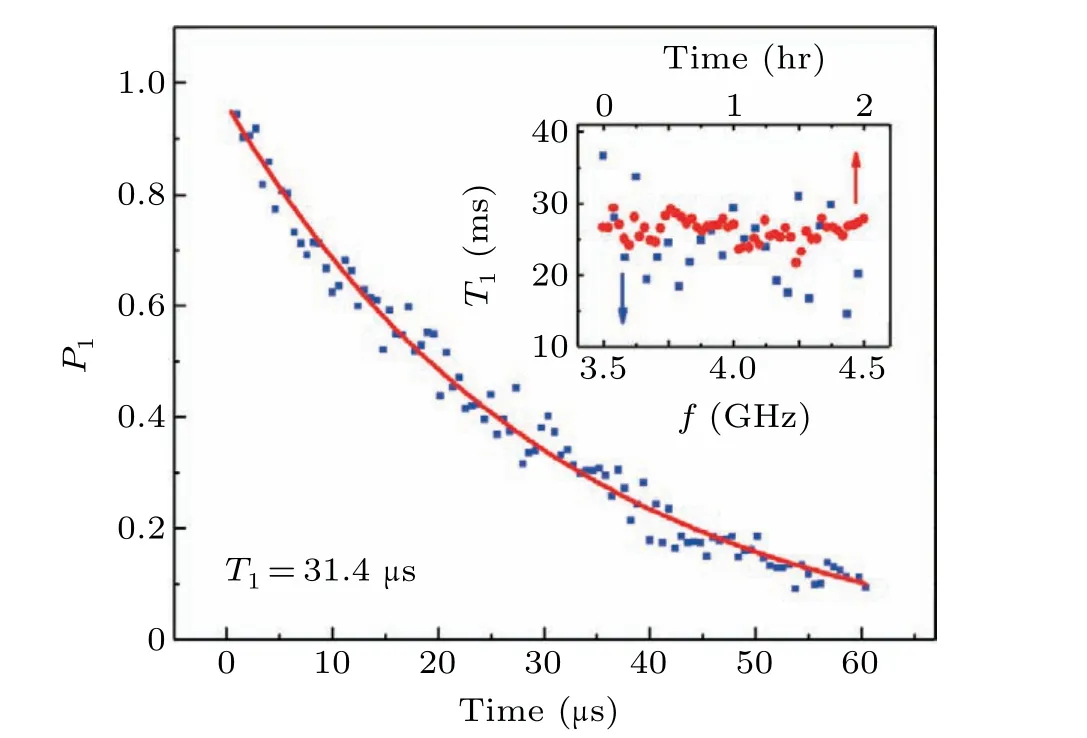
Fig.2. Experimental (symbols) and fitted(line) results of the energy relaxation process for qubit nine of sample II.The inset shows the variations of T1 with qubit frequency(squares)and time(circles).

Table 1. Energy relaxation time T1,Ramsey and spin-echo dephasing times Tϕ and T2E,measured near the qubit maximum frequency f01 for sample I.Data in parentheses are from sample II.
The qubit dephasing time can be determined from the Ramsey interference experiment, which measures the nondriven, freely precessing qubit state.[27]In this experiment aπ/2 microwave pulse around thex-axis tips the state vector from the north pole down to the equator, which is allowed to rotate in thex–yplane for a given timeτbefore being projected back by a secondπ/2 pulse. Furthermore, when aπpulse around thex-axis is inserted between the twoπ/2 pulses in the Ramsey experiment,a spin-echo experiment is performed,which removes the line-broadening associated with the lowfrequency noise of the qubit precession,and allows the observation of improved qubit coherence after the low-frequency dephasing noise has been mitigated. The measured dephasing time and characteristic time of the spin-echo experiment were up toTϕ=14.1µs andT2E=47.1µs,respectively. The typical measured values together withT1are listed in Table 1 for all qubits of sample I and qubit nine of sample II.
We characterize the single qubit gate fidelity by the randomized benchmarking method.[28,29]In this method, the qubit is first prepared in the ground state and a sequence ofmClifford gates are randomly chosen to drive the qubit. ThemClifford gates are either applied successively or interleaved with a specific gateH. The measurement of the remaining population of the initial state after the gate operations gives rise to the reference and gate sequence fidelitiesF, respectively, which can be fitted usingF=Apm+B, whereAandBare constants andpis a depolarizing parameter. In Fig. 3,we show the results forH=Y−π/2measured for qubit eight of sample I.For each sequence lengthm,we repeat the measurement 30 times(the open symbols represent their average values).By fitting to these values as a function ofm,we obtain the parametersprefandpgate. The gate fidelity is then calculated byFgate=1−(1−pgate/pref)/2 to be 99.86%. In Table 2,we list the experimental results for several other gate operations with fidelities as high as 99.97%in the case ofH=Xπ/2.

Table 2. Gate fidelities measured at f =4.979 GHz for qubit eight of sample I.

Fig. 3. Sequence fidelities as a function of the number of Clifford gates in a randomized benchmarking experiment for qubit eight of sample I.See text for further details.
Two-qubit vacuum Rabi oscillations are useful for the evaluation of the qubit coupling strength as well as calibrations of theZ-pulse amplitude and the iSWAP gate operation parameters.[30]Figure 4 shows the result when the frequency of qubit seven of sample I is fixed at 4.568 GHz and aZpulse with a changing amplitude is applied to qubit eight to vary its frequency near the resonant point with qubit seven.Qubits seven and eight are prepared in the ground and first excited states, respectively, and for eachZ-pulse amplitude,the excited-state populations of both qubits are measured as a function of time. In Fig. 4, we can see a clear excitation swap between the two qubits. At the central frequency, the fitted maximum period is 23.88 ns (or a minimum frequency of 41.88 MHz), which corresponds to a qubit–qubit coupling strength of 20.9 MHz.

Fig.4. Vacuum Rabi oscillation between qubits seven and eight of sample I.
For multiqubit devices and experiments, the crosstalk among qubits, i.e., the case in which one qubit is manipulated via theZand/orXYcontrol lines and other qubits also experience the change, is notorious, and greatly hinders qubit manipulation.[17,31,32]In this work, we fabricated Al airbridges across the control lines (see Fig. 1) to overcome this problem. Since a change of qubit frequency causes the resonator frequency to change, one can detect the crosstalk among qubits, for example, by varying the flux bias of one qubit and monitoring the resonator frequency changes of the other qubits. Figure 5 shows the results for sample III.When we change the flux bias of qubit eight,its resonator frequency shows periodic changes(middle panel)as expected,while the corresponding changes in the neighbouring qubits, seven and nine, can hardly be seen (left and right panels). A detailed analysis of theZ-pulse crosstalk matrix measurements indicates that the crosstalk among qubits is less than 1%.
Our results demonstrate that transom qubit devices with Nb films as their base electrodes fabricated using the simple fabrication process described above can have excellent properties and performance.We note that the experimentally determined device parameters,including the resonator frequencies,qubit-resonator coupling strength, qubit frequencies, as well as the qubit–qubit coupling strength measured by SWAP spectroscopy,are close to the designed values.The qubit coherence times are comparable to the results recently reported by the Princeton group using similar preparation conditions, which included an energy relaxation time ofT1=23µs.[33]Further improvements in the device coherence properties could be expected if more sophisticated substrate cleaning procedures and elevated substrate temperatures were used during the growth of the Nb film.[22,34–36]In addition, further optimizations of the device design and the use of alternative materials could improve the qubit performance beyond the limitations of the device fabrication process.[32,33,37–39]

Fig.5. Changes of the resonator frequencies from qubit seven to qubit nine of sample III (left to right panels) when only qubit eight is subjected to a changing flux bias,showing an extremely small crosstalk among qubits.
4. Summary
We have developed a fabrication process for superconducting transmon multiqubit devices with Nb base layers,shadow evaporated Josephson junctions, and airbridges for suppressing crosstalk among qubits. The fabricated multiqubit devices demonstrated excellent coherence properties,high gate fidelities, and small crosstalk. Two-qubit vacuum Rabi oscillations were measured to evaluate the qubit–qubit coupling strength. Our work provides a simple and convenient fabrication process, which could be useful for scaling up to more qubits, or the use of similar hard metal materials, such as Ta,for qubit fabrication. Further improvements in qubit coherence properties using these materials should be possible by modifying the substrate treatment and surface cleaning process, as well as by elevating the substrate temperature during film deposition.
Acknowledgment
We are grateful to the Laboratory of Microfabrication at the Institute of Physics for technical help.
猜你喜欢
杂志排行

Chinese Physics B的其它文章
- Physical properties of relativistic electron beam during long-range propagation in space plasma environment∗
- High winding number of topological phase in non-unitary periodic quantum walk∗
- Widely tunable single-photon source with high spectral-purity from telecom wavelength to mid-infrared wavelength based on MgO:PPLN∗
- Control of firing activities in thermosensitive neuron by activating excitatory autapse∗
- Adaptive synchronization of chaotic systems with less measurement and actuation∗
- Dynamics analysis of a 5-dimensional hyperchaotic system with conservative flows under perturbation∗