Electronic and magnetic properties of single-layer and double-layer VX2(X=Cl,Br)under biaxial stress∗
2021-10-28XingLi李兴YanfengGe盖彦峰JunLi李军WenhuiWan万文辉andYongLiu刘永
Xing Li(李兴), Yanfeng Ge(盖彦峰), Jun Li(李军), Wenhui Wan(万文辉), and Yong Liu(刘永)
State Key Laboratory of Metastable Materials Science and Technology&Key Laboratory for Microstructural Material Physics of Hebei Province,
School of Science,Yanshan University,Qinhuangdao 066004,China
Keywords: first-principles,biaxial tensile stress,phase transition,magnetic properties
1. Introduction
Since graphene[1]with weak interlayer van der Waals (vdW) interaction was successfully exfoliated, twodimensional (2D) materials have received extensive attention from scientists. Many 2D materials with excellent optical,[2,3]mechanical,[4]electrical,[5–7]and magnetic[8,9]properties have been widely studied, such as: phosphorene,[10,11]transition metal dichalcogenides (TMDs),[12,13]and CrI3.[14–16]Among them, 2D magnetic semiconductor materials have great potential in spintronic devices[17,18]due to their magnetic properties and ultra-thin thickness.
The large area and outstanding stretchability of 2D materials allow its magnetic properties be tailored by external field. For example, when an external electric field[19]is applied to this CrI3,electrons transporting through the CrI3barriers will generate huge magnetoresistance[15,16,20]due to the spin filtering effect. Songet al.proposed that the perpendicular electric field can adjust the splitting energy and reverse the spin splitting direction in the vdW monolayer arsenene/FeCl2heterostructures.[21]On the other side, stress engineering is also a common method to control the magnetic properties of 2D materials. The stress on the 2D material can be realized by the methods of substrate effect[22–24]and piezoelectric actuators[25,26]in the experiments. Zhuet al.pointed that the magnetic anisotropy energy of the 2D vdW GeS/FeCl2multiferroic heterostructures can be increased by applying biaxial compressive strain.[27]Zhanget al.found that there is a strain-induced phase transition from half semiconductor to bipolar magnetic semiconductor in the Janus Cr2I3X3(X=Cl,Br)monolayer.[28]When a biaxial tensile stress of 3.5%is applied to the single-layer of MoS2doped with single Fe atom,its magnetic moment changes from 2.04µBto 4µB.[12]Besides,there are phase transitions between the FM state and the AFM state in 2D materials[29–31]when stress is applied. For instance, when a biaxial compressive stress is applied, single layer CrI3[29]has a phase transition from FM state to AFM state,and single layer MnPSe3[30]has a phase transition from AFM state to FM state.
Inspired by the research of 2D material under external stress field, we put the research goal on 2D transition metal dihalides VX2(X= Cl, Br). There are three stable phases[13,32–34](T phase,H phase,and Tdphase)in the widely studied 2D TMDs.[35,36]Since 2D transition metal dihalides and TMDs differ only in non-metallic atoms, we also use the phases mentioned above to analyze 2D transition metal dihalide VX2. Several theoretical works[37,38]have displayed that the ground state of free-standing single-layer VX2in both 1H and 1T phases are AFM. In this work, we systematically investigated the mechanical, dynamic, electronic, and magnetic properties of single-layer and double-layer VX2under different stresses.Similar to previous work,[39]different stacking patterns are considered in constructing double-layer VX2.We find that the ground states of the single and double layer VX2are AFM semiconductors with T phase, and they are mechanically and kinetically stable. A phase transition from AFM state to FM state occurs when the biaxial tensile stress is applied. The mechanism of the magnetical phase transition is the competition between direct exchange and superexchange interactions. The band gaps increase and then turn to decreasing under biaxial tensile stress. Besides,applying stress to the VX2can increase the value ofTN.
2. Theoretical method
In the framework of density functional theory (DFT),the electronic structure and magnetic properties of materials were studied using the projector augmented wave (PAW)method, which was implemented in the Viennaab initiosimulation software package (VASP).[40,41]Perdew–Burke–Ernzerhof (PBE) was used to process the exchange relation function.[42]In this paper, a supercell size of 2×2×1 unit cells was used to study the magnetic structures in the calculations. A cutoff energy of 600 eV and aΓ-centered Monkhorst–Packk-points mesh of 9×9×1 for the Brillouin zone was found to be sufficient to obtain the convergence.The conjugate-gradient algorithm was employed for geometry optimization using convergence criterion of 10−6eV for the total energy and 0.01 eV/°A for Hellmann–Feynman force components. Using the density functional perturbation theory(DFPT)[43]to calculate the phonon spectrum,the convergence criterion of 10−10eV for the total energy and 10−5eV/°A for Hellmann–Feynman force components. We included the vdW correction in all the calculations using zero damping DFT-D3 method of Grimme.[44]
3. Results and discussion
The present work explores single-layer and double-layer VX2(X= Cl, Br) with the three most common phases in TMDs,namely T,H,and Tdphases.[13,32,34]Since the singlelayer and double-layer materials can be constructed by peeling off one or two layers from bulk materials, we need to construct the bulk structures at first. For the single-layer T-phase structure, there are three unequal positions (named A, B, C)in the c-axis direction, which are the position of one V atom and the positions of twoXatoms. And the single-layer Hphase structure has two unequal positions (named A, B) in thec-axis direction. Therefore, we could consider different stackings for the bulk structures. For example, AA stacking,AB stacking, and ABC stacking (stacking here only considers the different stacking methods of V atoms) are shown in Fig. 1 and Figs. A1–A3 in Appendix A: Supplemental material(See supplemental material for more details on the structures constructed, antiferromagnetic configurations of singlelayer structure, phonon spectrums, the formula for calculating the exchange correlation constant of double layer materials,and the exchange correlation constant of the ground-state single-layer and double-layer VX2). The bulk T-phase structure (ABC stacking) has hexagonal lattice, which belongs to theR3mspace group(166). In calculations,the non-magnetic(NM),FM,and AFM states are considered,by optimizing the atomic position and lattice constant to fnid the lowest energy states. The structures of Tdphase and T′phase would turn to the corresponding stacking forms of T phase when magnetism is considered, and the only difference between Td-phase and T′-phase structures is the stacking. In the following calculations,we only consider the T-phase and H-phase structures.
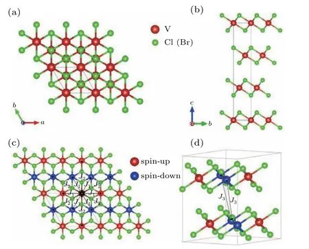
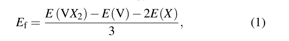
Fig.1. The schematic diagrams of the ground-state structure of the bulk transition metal dihalide VX2 (X =Cl, Br) in the c direction(a)and a direction(b). The ground-state AFM configurations of single-layer (c) and doublelayer (d) transition metal dihalide VX2 (X =Cl, Br), respectively. J1 and J2 represent the exchange correlation constant of the nearest neighbor and next-nearest neighbor in the layer,and J3 represents the exchange correlation constant of the third nearest neighbor between the layers.
The cleavage energy is the energy required to cleave the bulk materials in two halves,[45]which is a criterion for judging whether the bulk material is easy to peel off. The formula used to calculate the cleavage energy givesEc=Es−Et,whereEsdenotes the total energy of two separate parts andEtdenotes the total energy of the bulk. We find that the cleavage energy(see Table 1)of all structures considered in the article are less than that of graphene[46](0.36 J/m2), so they are easy to be peel off. Furthermore,the formation energy determine the difficulty for sythesision of VX2. For the binary compound VX2,the expression for the formation energy can be written as
whereE(V),E(X),andE(VX2)are the normalized energy of the stable bulk bcc-V, gas phases (Cl2, Br2), and bulk VX2,respectively. See Table 1, since the formation energies of all stuctures considered in this paper have negative values,which are experimentally stable.

Table 1. A summary table of the formation and cleavage energy of bulk VCl2 and VBr2. Ec stands for cleavage energy and Ef stands for formation energy.
In order to determine the most stable phases in all structures, one NM, one FM, and four AFM configurations are considered for the single-layer structure. For the double-layer structure,one NM,one FM,and seven AFM configurations[47]are considered. We find that the T-phase of the single-layer structure has lower formation energies, and the ground state magnetic order (named AFM2) is shown in Fig. 1(c) which is consistent with previous work.[37,38]The ABC stacking double-layer structure with T phase is more stable, and the ground-state AFM configuration is shown in Fig.1(d). In Table 2,the NM state has higher energy than the magnetic state,only the corresponding AFM configuration of the ground state is considered in the following calculations. Furthermore, in order to test the dynamic stability of the ground state singlelayer and double-layer structures,we provide the corresponding phonon spectrums in Fig.A5. There is no imaginary frequencies,implying the kinetic stability of the single-layer and double-layer VX2.
Figure 2 shows the electronic band structures and project density of states(PDOS)of the ground-state phases(the structure shown in Fig. 1). The indirect band gaps of the doublelayer VX2(1.0276 eV forX=Cl, 1.0170 eV forX=Br)is smaller than that of the single-layer VX2(1.0713 eV forX=Cl, 1.0472 eV forX=Br). Further, the electronic band structure of the double-layer structure is different from that of the single-layer structure in theKtoΓrange. The electrons of the d orbital of the V atom that play a major role to the band structure in this range. Due to the coupling between the layers, the electrons are not only localized in the plane, but also a small amount of electrons in a small range close to the plane, which leads to the difference in the band structure betweenKandΓ. The density of states (DOS) of all materials near the Fermi energy is reduced to zero,make these materials semi-conductivity.

Table 2. The normalized energy table of the ground state(AFM state),FM state,and NM state of single-layer and double-layer VX2 (X =Cl,Br). s-T represents single-layer T-phase structure,and d-T represents double-layer T-phase structure.

Fig.2. The ground-state electronic band structures and project density of states(PDOS)of(a)s-T-VCl2,(b)d-T-VCl2,(c)s-T-VBr2,and(d)d-T-VBr2.
For the 2D material VX2(X=Cl, Br), the microscopic mechanisms of VX2,which determine the magnetic properties,contain two parts: (i) direct AFM exchange interaction between two V atoms;(ii)FM superexchange interaction among V–Cl(Br)–V with an anionic mediation Cl(Br). The competition between AFM and FM may lead to different magnetic ground state. When the direct exchange interaction between two V atoms is stronger than the superexchange interaction between V–Cl(Br)–V,the ground state of the material shows AFM, otherwise it is FM. Here, the direct exchange interaction between V atoms is dominant in these systems. For AFM materials,the N´eel temperature(TN)[48,49]refers to a parameter of the temperature at which the AFM phase of the antiparallel magnetic order changes to the NM phase. We use the Ising model in the Monte Carlo method to calculate it. The Hamiltonian[50]can be written in the following form:

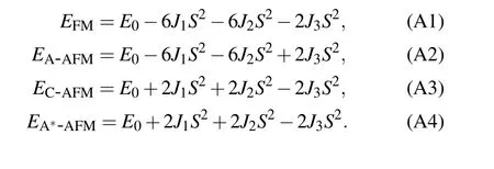
whereJijrepresents the exchange interactions of over all neighbor V–V pairs,Sirepresents the spin of the atomi.For the single-layer structure, this paper considers the nearest neighbor and the next nearest neighbor interaction,and the third nearest neighbor interaction between the layers is also considered for the double-layer structure. To calculateJ, we write the energy of the single-layer VX2in the FM, AFM2,and AFM4 configurations(shown in Fig.A4)in the following form:
whereJ1andJ2(shown in Fig. 1(c)) represent the exchange correlation constant of the nearest neighbor and the next nearest neighbor,andE0is the energy of a single-layer VX2without spin polarization andS=3/2.[51]Through calculations,the absolute value ofJ1for all materials is much greater thanJ2(J3),and the value ofJ1is negative(in the Table A1),which further verifies the antiferromagnetism of the ground states.We use the Metropolis algorithm and a 32×32 2D supercell with periodic boundary conditions to computeTN,and the calculations are implemented in mcsolver software.[52]Besides,because 2D materials have excellent stretchability, the pressure factor is also taken into account in the calculations. Figure 3 shows that the Monte Carlo simulations ofTNof the single-layer and double-layer VX2with pressure. When no stress is applied,theTNof single-layer and double-layer VCl2is 62 K and 96 K, and the value of single-layer and doublelayer VBr2is 32 K and 144 K.Compared with the single-layer VX2, theTNof the double-layer VX2are higher. In Table 2,the normalized energy of the double-layer structure is lower than that of the single-layer structure, so the coupling effect between the layers makes the double-layer systems more stable and higherTN. When stress is applied to the materials,as the stress increases,theTNof all materials tend to increase.
Further,we calculate the Curie temperature(Tc)of the ferromagnetic state under a tensile stress of 8%,theTcof singlelayer and double-layer VCl2is 53 K and 24 K, respectively.Due to the 8% stress is close to the phase transition point of single-layer and double-layer VCl2, the small exchange correlation constant results in a low Curie temperature. TheTcof single-layer and double-layer VBr2is 175 K and 293 K,respectively. The latter one is close to the room temperature.

Fig.3. (a) The N´eel temperature of single-layer and double-layer VCl2 and VBr2 under stress. (b) The Curie temperature of single-layer and doublelayer VCl2 and VBr2 under 8% biaxial tensile stress, m represents the total magnetic moment per V atom.
We also explore the magnetic state, magnetic moment and band gap depends of biaxial stress. From Fig. 4(a), the ground states of all materials change from an AFM state to an FM state when the biaxial tensile stress reaches the corresponding critical point. Meanwhile, there are no phase transitions under biaxial compressive stress. The stress of the phase transition points of the single-layer and double-layer VCl2are 6.65%and 7.64%,while the single-layer and doublelayer VBr2are 4.49%and 5.32%. For the same material, the phase transition stress for a double-layer structure is greater than that of a single-layer structure. See Fig. 4(b), the band gaps also changes under by applying biaxial stress. When applying pressure, the band gaps of all materials gradually decrease. However, when stress increases, the band gaps of all materials firstly become larger and then turn smaller. Noted that the band gaps decrease rapidly near the phase transition point. In Fig. 4(c), we find that the magnetic moment gradually decreases and increases under biaxial compressive and tensile stress, respectively. As the spin-polarized charges of VX2(X=Cl and Br)mainly arise from the localized nonbonding V-3d electrons,the increase of tensile stress reduces the covalent interaction between V and Cl or Br atoms. As a result,the number of nonbonding V-3d electrons increases, so that the magnetic moment of V atomic increases.[53]On the other side,compressive stress has the opposite effect. Moreover,the magnetic moment jumps at the phase transition points,and becomes insensitive to stress after the phase transition points.

Fig.4. (a)Magnetic ground state,(b)band gap,and(c)magnetic moment of single-layer and double-layer VCl2 and VBr2 under biaxial stress.
4. Conclusion
In summary, we explore the ground state phases among the possible structures of single-layer and double-layer VX2(X=Cl, Br)based on first-principles calculations. The electronic and magnetic properties of the corresponding phase under biaxial stress are systematically investigated. The ground states of single-layer and double-layer VX2are all AFM semiconductors with T phase, and are dynamically and mechanically stable. All ground-state structures only have one phase transition from AFM to FM under biaxial tensile stress. The mechanism of the magnetic phase transition is the competition between direct exchange and superexchange interactions.The band gaps increase and then turn to decreasing under biaxial tensile stress.TNof the single-layer are lower than that of double-layer VX2according to Monte Carlo simulations,which may be caused by the coupling effect between the layers. Besides,applying stress to the VX2can increase the value ofTNand the magnetic moment increases as the biaxial tensile stress increases. In 2015,Lvet al.[54]summarized controlled synthesis of 2D TMDs using wet chemical approaches,chemical exfoliation,and chemical vapor deposition(CVD).Meanwhile,it is possible to control the number of layers when synthesizing these materials. Our results show that single-layer and double-layer VX2(X=Cl, Br) would possess potential applications in spintronic devices. We also hope that our theoretical research will be helpful to the further experiment.
Acknowledgment
Thanks to the teachers and classmates who have helped me,and thanks to my parents and friends for their supports.
Appendix A:Supplemental material
In order to better understand and explain the descriptions in the main text, some figures, formulas, and table are given below.

Fig.A1. The schematic diagrams of the bulk T-phase VX2(X=Cl,Br)of(a)AA stacking and(b)AB stacking.

Fig. A2. The schematic diagrams of the bulk H-phase VX2 (X =Cl, Br) of(a)AA stacking and(b)AB stacking.

Fig.A3.The schematic diagrams of the bulk VX2(X=Cl,Br)of(a)T′-phase and(b)Td-phase.

Table A1. The exchange correlation constants of the ground-state singlelayer and double-layer VX2.

Fig. A4. The antiferromagnetic configurations of single-layer VX2 of (a)AFM1,(b)AFM3,and(c)AFM4.

Fig.A5. Phonon spectrum of the ground-state single-layer and double-layer(a)VCl2 and(b)VBr2.

Fig.A6. Phonon spectrum of the ground-state single-layer and double-layer(a)VCl2 and(b)VBr2 under 10%tensile stress.
The formulas for calculating the exchange correlation constants of double layer materials are given below:
猜你喜欢
杂志排行

Chinese Physics B的其它文章
- Physical properties of relativistic electron beam during long-range propagation in space plasma environment∗
- High winding number of topological phase in non-unitary periodic quantum walk∗
- Widely tunable single-photon source with high spectral-purity from telecom wavelength to mid-infrared wavelength based on MgO:PPLN∗
- Control of firing activities in thermosensitive neuron by activating excitatory autapse∗
- Adaptive synchronization of chaotic systems with less measurement and actuation∗
- Dynamics analysis of a 5-dimensional hyperchaotic system with conservative flows under perturbation∗