Surface plasmon resonance characteristics of a graphene nano-disk based on three-dimensional boundary element method
2021-10-10WANGShuoHUBinLIUJuan
WANG Shuo,HU Bin,LIU Juan
(School of Optics and Photonics, Beijing Institute of Technology, Beijing 100081, China)
* Corresponding author,E-mail: hubin@bit.edu.cn
Abstract: Compared with the commonly used simulation algorithms such as Finite Element Method (FEM)and Finite-Difference Time-Domain (FDTD) method, the Boundary Element Method (BEM) has the advantages of high accuracy, small memory consumption, and ability to deal with complex structures. In this paper,the basic principle of three-dimensional BEM is given, the corresponding program based on C++ language is written, and the Surface Plasmon Resonance (SPR) characteristics of a graphene nano-disk structure are studied. The Scattering Cross-Section (SCS) spectral lines of a graphene nano-disk under different chemical potentials, as well as the distributions of electromagnetic fields at the resonance wavelengths are calculated. The electromagnetic response of the graphene nano-disk in the infrared band is analyzed. In addition, considering the common corrugations of graphene materials caused by defects during processing, we study the influence of the geometric parameters of a convex structure in the center of the graphene nano-disk on the resonance intensity, wavelength and field distributions. A spring oscillator model of charge movement is used to explain the simulation results.
Key words: three-dimensional boundary element method; graphene; surface plasmon resonance; scattering characteristics
1 Introduction
When light is incident on the metal surface, the free charges in the metal will be driven by the incident light field to form collective oscillations with strong scattering, absorption or coupling. This characteristic is called Surface Plasmon Polaritons(SPPs) resonance. The SPPs have a strong local field enhancement effect. Because their transmission wavelength is smaller than that of incident light, they can be used in optical waveguide[1], lithography[2]and other fields. When the metal size is reduced to tens or hundreds of nanometers, the electromagnetic wave transmitted along the surface will be confined on the surface, generating Localized Surface Plasmonic Resonance (LSPR). Since the resonance wavelength, resonance intensity and scattering spectrum of LSPR can be modulated by the material, shape and other factors of nanostructures,LSPR has been widely studied and applied in the fields such as biosensing[3], energy[4]and information[5].
Graphene is a two-dimensional crystal made of a single layer of carbon atoms linked into honeycomb lattices[6], and is a good LSPR material with strong local field enhancement effect and low loss.In addition, the properties of graphene can be adjusted by the methods such as chemical doping and applied electric field, so graphene can be made into a new type of LSPR optical device with external modulation[6]. Graphene has a broad application prospect in optical waveguides[7-9], biosensors[10], metasurfaces[11], metamaterials[12,13], photoelectric devices[14]and other optical fields. Graphene nanodisk is a commonly used graphene structure. C.X.Cong et al.successfully prepared an ordered graphene nanodisk array by combining nanospheric lithography with reactive ion etching[15]. Sukosin Thongrattanasiri et al. investigated the application of graphene nanodisks in optical absorption and demonstrated a periodic graphene nanodisk array capable of achieving 100% optical absorption[16]. Zheyu Fang et al.proposed a tunable optical absorber based on graphene nanodisks and investigated the relationship between its absorption characteristics and the size, spacing and chemical potential of the nanodisks[17]. Hugen Yan et al. studied the coupling effect of graphene nanodisks and proved that different coupling modes would lead to different electromagnetic responses[18]. Jialong Peng et al. reported the study of a tunable terahertz half-wave plate based on coupled graphene nanodisks, using a reflective structure to achieve the function of half-wave plate[11]. Lauren Zundel et al. achieved infrared molecular sensing with subwavelength-level spatial resolution by utilizing the electrical tuning properties of the plasmon polaritons of graphene nanodisk arrays[19]. Vasilios D. Karanikolas et al. studied the role of graphene nanodisks between quantum emitters and demonstrated that the strong resonance of graphene nanodisks could increase the interaction distance between quantum emitters by an order of magnitude[20].
However, all of these studies focused on the ideal planar graphene. As a kind of flexible material,graphene can produce convex/concave structures,corrugations and other non-planar defects in the machining process.
Meanwhile, with the progress of modern micro-nano machining technique, the three-dimensional structures with surface corrugations can also be fabricated by artificial stretching, squeezing, mechanical vibration and other methods, and their dimensional parameters can be controlled[21-23]. These three-dimensional structures can also modulate the SPP resonance of graphene. Penghong Liu et al.studied the SPP resonance mode of wedge-shaped graphene waveguides and obtained the SPP propagation constants and local field distributions in different modes[8]. Slipchenko et al. studied the SPP reflection properties of corrugated graphene layers and quantitatively described the effect of corrugations on the reflection intensity[24]. Shengxuan Xia et al. demonstrated the tunable electromagnetically-induced transparency of sinusoidal graphene layers[25].Li Wang et al. investigated the LSPR properties of bent graphene nanoribbon arrays molded on soft substrates and discovered a new decoupling mechanism[26]. However, the above studies were all based on two-dimensional structures. There are few reports on the non-planar graphene with a three-dimensional defect structure.
In this paper, the three-dimensional boundary element method (3D-BEM or BEM) was used to study the SPR properties of flat and convex graphene nanodisks. Compared with other simulation algorithms in common use, the 3D-BEM can simplify the calculation of three-dimensional objects into the solution of the surface field of objects,that is, it can reduce the three-dimensional calculation to two-dimensional calculation. Therefore, this method can reduce the occupation of computer resources, and improve the calculation speed. We have written a 3D-BEM numerical calculation program based on C++ language. From the calculation results, it can be seen that the incident light in the mid-infrared band can stimulate the SPR phenomenon of graphene structure. By adjusting the electrochemical potential of graphene, we found that the resonance wavelength, the scattering intensity, and the FWHM (Full Width at Half Maximum) of the spectral lines all changed regularly. By adding a convex structure to the graphene structure, the scattering spectrum can also be shifted. We have made necessary explanation of the change law given in this paper by using the law of charge motion and the spring oscillator model. Our research will help understand the LSPR properties of graphene, and also expand the application of BEM algorithm.
2 3D-BEM theory
The schematic of scattering in three-dimensional space is shown in Fig. 1. In an isotropic free space, there is a three-dimensional scatterer, which is hit by infinite incident light. The scatterer surfaceSdivides the scatterer space into two parts, namely the outer regionV2and the inner regionV1. The outer normal vector of the scatterer is →n. The refractive index, relative dielectric constant and permeability of the regionV1aren1,ε1andμ1, respectively. The refractive index, relative dielectric constant and permeability of the regionV2aren2,ε2andμ2, respectively.
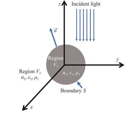
Fig. 1 Schematic of three dimensional scattering图 1 三维空间散射示意图

Fig. 2 Graphene model and surface-element division method (a) Graphene nanodisk model; (b) convex graphene nanodisk model; (c) mesh generation of graphene nanodisk model; (d) outer normal vectors of the meshes generated in graphene nanodisk(shown by blue arrows)图 2 石墨烯模型以及面元划分方法(a)石墨烯圆盘模型;(b)凸起石墨烯圆盘模型;(c)石墨烯圆盘建模的网格划分;(d)石墨烯圆盘所建网格的外法向矢量(蓝色箭头所示,见网络彩图)
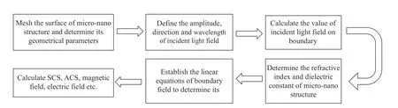
Fig. 3 Flow chart of boundary element method图 3 边界元算法流程图
By combining the classical Maxwell's equations with Green's function of vector potential, the following equations can be derived to show the distribution of electric and magnetic fields in the whole space[27]:
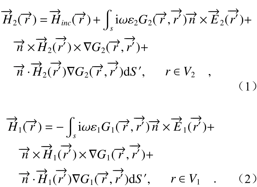


Next, we present the numerical method ofFirstly, the vector equations (3)and (4) are decomposed inx,yandzdirections to obtain 6 scalar equations[29], as shown in the appendix. Secondly, the surface of the scatterer is discretized and then divided intoMsurface elements.By using the values of electric and magnetic fields at the center of a surface element to approximate the electric and magnetic field distributions of the whole surface element, we can express the 6 scalar integral equations in the form of summation. Thus we can obtain the linear equation set of 6Munknowns[29], namely A6M×6MX6M=B6M. The 6Munknowns are the three components ofandin every surface elements, respectively, as shown in the appendix. Finally, by solving the linear equations, we can obtain the electric and magnetic field values of each surface element. It is worth noting that the calculated electric field value is only the tangential component of the actual electric field.
After the distributions of electric and magnetic fields on the surface of the scatterer are obtained,the magnetic field at any point in space can be obtained by further discretizing the equation (1) and equation (2). Then, by using Maxwell's equationthe electric field at this point can be calculated, and the distributions of electric and magnetic fields in the whole space can be obtained.After that, we can calculate other physical quantities, such as Scattering Cross Section (SCS), Absorption Cross Section (ACS), etc.
The SCS and ACS can be calculated by using the equations (5) and (6)[30]:
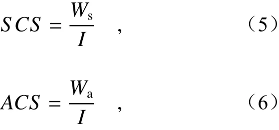
whereWsandWaare the scattering power and the absorption power. They can be calculated by using a closed surfaceГsurrounding the scatterer and the energy flux density (Poynting vector):


3 Modeling of the graphene nonadisk
We first consider the graphene nanodisk structure, with a diameter ofd=60 nm, located in thex-yplane, as shown in Figure 2(a). To study the graphene structure with a defect, we assume that there is a bulge at the center of the graphene nanodisk. This convex structure can be obtained by the mechanical vibration of a resonator[23]. The height of the bulge ish, as shown in Figure 2(b). The width of the bulge, marked as “w”, is defined as the length when the height is changed intoh/exp(1). Then the coordinates of the wrinkled nanodisk in thezdirection can be described as:
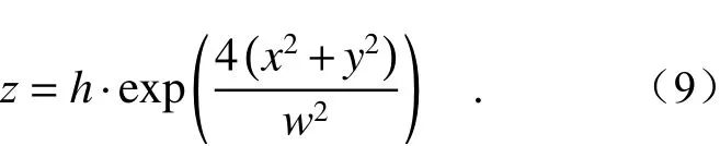
Next, we need to divide the surface elements of the graphene nonodisk structure through mesh generation. In the modeling process, the graphene thickness is set as 1 nm[32]. We consider the graphene nanodisk as a cylindrical model with very small height. Since the thickness of two-dimensional graphene material is very small relative to the size of the whole structure, the calculation instability can be caused easily. Therefore, an appropriate mesh generation method should be selected. The mesh generation here mainly follows the following two principles. Firstly, the aspect ratio of each mesh must not be too large. The maximum aspect ratio in this paper is 1.5:1. The structural change in the edge area is more complex than that in the central area, so the edge meshes should be denser. According to these two principles, meshes are generated in the disk, as shown in Figure 2(c). The upper and lower surfaces are divided into 11 rings. The width of each ring and the number of surface elements are shown in Table 1.
The flank is divided into two layers, each of which has 116 surface elements. Therefore, there are 1224 surface elements in total. The position of the center point of each face element and its outer normal vector are shown in Figure 2(d) (Color online). The mesh generation in a convex structure is realized by projecting the meshes of flat disk structure onto the convex structure along thezaxis.

Tab. 1 Parameters of mesh generation on the upper and lower surfaces of graphene nanodisk表 1 石墨烯纳米圆盘上下表面网格划分参数
The optical parameters of graphene are calculated using the method in the reference [32]. Its dielectric constant can be calculated by the following equation:

whereε0is the vacuum dielectric constant,ωis the angular frequency of the incident light,σis the conductivity of graphene, i is the imaginary unit, andtis the thickness of graphene. The conductivity of graphene in the far-infrared and terahertz bands can be expressed as[7,33]:

whereeis the charge per unit,EFis the chemical potential of graphene, andτis the carrier relaxation time.
Our numerical calculation program is written in C++ language. Under the sub-surface element condition mentioned above, the program occupies about 1.6 G of memory. It takes about 5 minutes for an ordinary personal computer (configuration: i7-8550U,4.0 GHz, 8G RAM) to calculate a wavelength point.The calculation process of the whole algorithm is shown in Figure 3.
4 Simulation results and analysis
4.1 Comparison of the results from BEM and FDTD
In order to verify the correctness of the threedimensional boundary element program written, we first calculated the SCS spectrum of graphene nanodisk in the wavelength range of 5~11 μm and the electric and magnetic field distributions at the resonant position, and then compared the results obtained by BEM with those obtained by the commercial software Lumerical FDTD Solutions based on Finite-Difference Time Domain (FDTD) method. The graphene disk under calculation has a diameter ofd=60 nm and a chemical potential ofEF=0.25 eV.The incident light perpendicular to the disk and incident along the −zaxis is linearly polarized light,and the polarization direction of electric field is along theyaxis. The normalized SCS spectra of the two algorithms are shown in Figure 4(a) and Figure 4(d) respectively. It can be seen that, in the calculated band, only one scattering resonance peak is obtained in either of the two algorithms. The resonant peaks in BEM and FDTD are at 7.04 μm and 7.3 μm, respectively, with the relative error of 3.6%.
The electric and magnetic field distributions calculated by BEM and FDTD under the resonant wavelength are shown in Fig. 4(b)~4(c) and 4(e)~4(f), respectively. By comparison, it can be seen that the electric and magnetic field distributions obtained by the two methods are very similar.For the electric field, the corresponding light fields are mainly concentrated in the two areas along the polarization direction of the incident light (ydirection). The magnetic field distribution is perpendicular to the electric field. This is mainly because the electric field component of the incident light forces the free electrons inside the graphene to oscillate collectively in the direction of electric field to form the plasmon resonance. Therefore, the resonant peaks in Figures 4(a) and 4(d) are the enhanced scattering phenomena caused by the SPR of graphene.

Fig. 4 Comparison of the results from BEM and FDTD. (a) SCS spectrum obtained by BEM; (b) magnetic field distribution obtained by BEM under the resonance wavelength; (c) electric field distribution obtained by BEM under the resonance wavelength; (d) SCS spectrum obtained by FDTD; (e) magnetic field distribution obtained by FDTD under the resonance wavelength; (f) electric field distribution obtained by FDTD under the resonance wavelength图 4 边界元算法与有限时域差分算法结果对比图。(a)边界元获得的SCS谱线;(b)共振波长下边界元获得的磁场分布;(c)共振波长下边界元获得的电场分布;(d)有限时域差分获得的SCS谱线;(e)共振波长下有限时域差分获得的磁场分布;(f)共振波长下有限时域差分获得的电场分布
4.2 Dependence of SCS spectrum on the chemical potential of graphene
One advantage of graphene over other materials is that its chemical potential can be dynamically adjusted by an applied electric field and other methods. Therefore, we calculated the influence of the change of chemical potential on the scattering characteristics of a graphene disk, without changing other parameter settings as shown in Figure 4. The chemical potentialEFwas set as 0.1, 0.15, 0.2 and 0.25 eV respectively. The calculation results are shown in Figure 5(a). It can be seen from the calculation results that, with the increase of chemical potential, the resonance wavelength is blue-shifted, the scattering intensity gradually increases, and the resonance peak width gradually decreases.
According to the reference [17], the relationship between the plasmon resonance frequency and electrochemical potential of graphene is ωp~(EF/D)1/2. Therefore, as the chemical potential of graphene increases, the resonant angular frequency will increase and the resonant wavelength will be blue-shifted. The number of charge carriers and the density of free charges gathered at both ends of the disk will increase with the chemical potential of graphene, leading to stronger scattering field intensity. The spring oscillator model presented in[32, 34] can explain many SPR phenomena. The scattering spectrum and absorption spectrum in the models meet the following linear law:
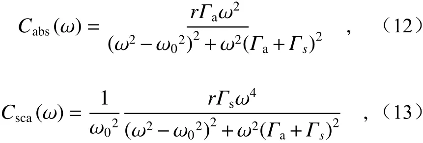
whereris the parameter related to structure and material, and Γaand Γsare the absorption coefficient and scattering coefficient respectively.
Since the SCS spectrum obtained by calculation is similar to the ACS spectrum, we only use the SCS spectrum to study the properties of graphene structure. By fitting the equations (12) and (13) with the ACS spectrum and SCS spectrum, we can obtain the scattering coefficientГsand the absorption coefficientГa. It is worth noting that since only the equation (13) is used to fit the scattering spectrum to obtain three relevant parameters, we should pay attention to the way of fitting and combine equation(13) with equation (12) in order to obtain accurate results. Ifω=ω0, both the SCS and ACS will be peaks, and the results will be as follows:
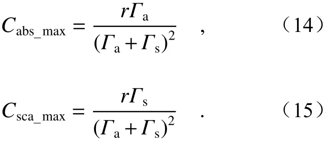
From the above two equations,andcan be obtained.Cabs_maxandCsca_maxcan be obtained from the scattering and absorption spectra. Therefore, we can fit the one parameterГsonly through equation (13), and obtain accurate results.
In Fig. 5(b), we show the relationship between the scattering coefficientГsand the chemical potential. It can be seen thatГsincreases with the chemical potential, which further explains the change rule of the scattering intensity. Also as shown in [32], for the narrow-band model structure of graphene in our paper, the scattering coefficient is directly proportional to the square of the charge involved in resonance and inversely proportional to the square of the resonance wavelength. This can also explain the change rule of the scattering coefficient. According to Reference [32], the half peak width of the scattering spectrum is directly proportional to the extinction coefficientГand the square of the wavelengthλ, that is, Δλ~Γ·λ2, where the extinction coefficientГis the sum of the scattering coefficientГsand the absorption coefficientГa. The relationship between the physical quantity Γ·λ2and the chemical potential is given in Figure 5(c). The physical quantity will decrease with the increase of chemical potential, thus explaining the change rule of half peak width.

Fig. 6 Influence of convex shape on SCS spectrum. (a) Relationship between SCS spectrum and convex height; (b) relationship between SCS spectrum and convex width图 6 凸起的形状对SCS谱线的影响。(a)SCS谱线与凸起高度的关系;(b)SCS谱线与凸起宽度的关系
4.3 Scattering spectrum changing with convex shape
In practical use, graphene may exhibit structural deformation due to the reasons mentioned earlier.Therefore, we also considered the influence of nonplanar convex structure on the LSPR of graphene.We calculated a disk-shaped planar graphene structure (as shown in Figure 4) with a bulge in the center and a chemical potential ofEF=0.2 eV. At first,the total width of the bulge was set as 20 nm, and its height was set as 10, 20, 30, and 40 nm respectively.The SCS spectrum results were obtained, as shown in Figure 6(a). We found that, with the increase of the bulge height, the resonance peak moved to the long-wave direction, resulting in a red shift. At the same time, the resonance peak intensity increased.The red shift of the resonance wavelength was mainly caused by two reasons. First, with the increase of the bulge height, the path of charge movement from one end of the graphene structure to the other end became longer[32]. Second, as the charge passed through the bulge, it could only be driven by the component of the electric field of the incident light in the direction of the path. Therefore, the increase of the bulge height led to the decrease of the charge-driving force, thereby slowing down the response of a charge to the incident light field[26]. That is to say, the bulge hindered the movement of the charge. Both reasons led to a longer cyclical movement period of the free charge, a lower resonance frequency and a red shift of the resonance wavelength. On the other hand, the increase of scattering intensity was possibly caused by the increase of the bulge height, which might lead to the increase of charge carriers inside the graphene and the increase of the charges gathering at both ends of the graphene structure to form a stronger scattering field. From this, we inferred that if the height of the bulge was fixed and its width was changed, a similar changing trend could also be generated to cause a resonance red shift and enhanced scattering. Then we did the calculation and obtained the results shown in Figure 6(b). We set the height ash=30 nm and the width changing from 10 nm to 20.5 nm. The calculation results were similar to what we expected, except that the SCS spectrum had no significant change until the bulge width was more than 18 nm.
5 Conclusion
In this paper, the SPR properties of the graphene nanodisk were studied by using the boundary element method. We established the numerical model of the geometrical structure of a graphene nanodisk, wrote a 3D-BEM algorithm based on C++language, and calculated the scattering spectrum of the nanodisk and its electric and magnetic field distributions at resonant wavelength.At first, we compared the results obtained by BEM with those obtained by the commercial software based on FDTD and verified the correctness of our program. Then we calculated the scattering spectra of the graphene disk under different chemical potentials. We found that with the increase of chemical potential, the resonance wavelength was blue-shifted, the scattering intensity increased, and the resonance peak width decreased gradually. Finally, we added a convex structure to the original graphene nanodisk model,and considered the influence of the convex structure on the scattering properties of graphene. Our research will contribute to the understanding of the physical law of graphene LSPR and the influence of surface corrugations on the LSPR phenomenon.
——中文对照版——
1 引 言
当光照射到金属表面,金属内的自由电荷在入射光场的驱动下形成集体震荡,表现出强烈的散射、吸收或者耦合,这个特性称为表面等离子体激元共振(Surface Plasmon Polaritons, SPPs)。SPPs具有很强的局域场增强效应,由于其传导波长比入射光小,因此可以应用于光波导[1]、光刻[2]等领域。当金属尺寸缩小至几十纳米或者几百纳米时,沿表面传导的电磁波将会被束缚在表面,形成局域表面等离子体共振(Localized Surface Plasmonic Resonance, LSPR)。由于LSPR的共振波长、共振强度、散射谱线等能够通过改变纳米结构的材料、形状等因素调节,所以在生物传感[3]、能源[4]、信息[5]等领域被广泛研究和应用。
石墨烯是由碳原子按蜂窝晶格链接而成的单原子层二维晶体[6],是一种良好的LSPR材料,可以实现超强的局域场……
猜你喜欢
杂志排行
中国光学的其它文章
- A new automatic cell smear and laser release system for near-infrared light responsive release of nucleated red blood cells
- Design of optical wedge demodulation system for fiber Fabry-Perot sensor
- Photon-assisted Fano resonance tunneling periodic double-well potential characteristics
- Formation mechanism of the continuous spectral profile of lightning plasma
- 中国遥感卫星辐射校正场敦煌戈壁场区光环境变化研究
- 油气井下光纤光栅温度压力传感器