GaAs器件镀层应力问题分析及解决
2021-08-24王敬松周国
王敬松 周国
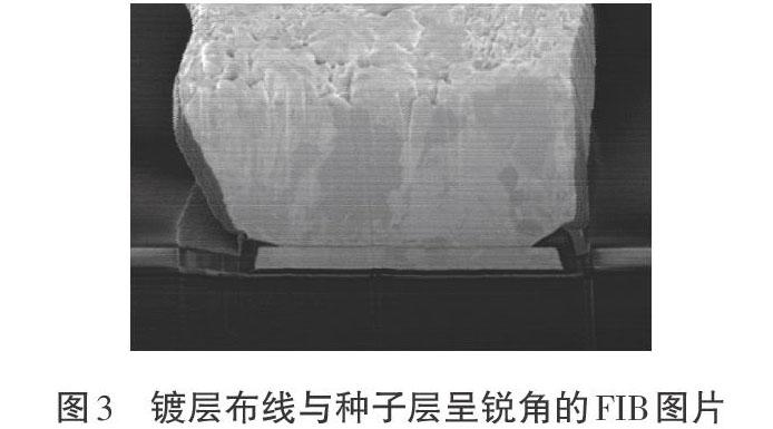
摘 要:传统的GaAs电镀布线工艺,镀层金属与种子层呈锐角,导致氮化硅表面出现变色脱落等现象,影响器件稳定性和可靠性。本文改进了传统的电镀布线工艺,在电镀布线后,表面先涂覆薄层聚合物(0.5 μm以内)以消除锐角,消除应力集中点,之后再淀积氮化硅,形成复合保护层。改进后的工艺解决了因镀层金属应力集中导致的氮化硅表面变色和脱落等问题。
关键词:电镀布线;应力集中;氮化硅
中图分类号:TN304.23文献标识码:A文章编号:1003-5168(2021)10-0033-03
Analysis and Solution of Coating Stress on GaAs Device
WANG Jingsong ZHOU Guo
(The 13th Research Institute of China Electric Technology Group Corporation,Shijiazhuang Hebei 050051)
Abstract: In the traditional GaAs electroplating wiring process, the coating metal and seed layer have an acute angle, which leads to the phenomenon of discoloration and falling off on the surface of silicon nitride, which affects the stability and reliability of the device. In this paper, the traditional electroplating wiring process is improved. After the electroplating wiring, a thin layer of polymer is coated on the surface to eliminate the acute angle and stress concentration point, and then silicon nitride is deposited to form a composite protective layer. The improved process solves the problems of discoloration and peeling of silicon nitride surface caused by stress concentration of coating metal.
Keywords: electroplating wiring;stress concentration;SiN
GaAs(Gallium Arsenide,砷化镓)器件具备高电子迁移率、高电子饱和漂移速度等优点,在雷达、航空航天、通信、功率电子等领域都具有广阔的应用前景。随着5G时代的到来,对无线通信终端和通信基站等微波系统的收发组件提出了更高的要求。而利用GaAs材料制作的低噪声器件具有效率高、抗辐射能力强等优点,将其应用于通信领域,能满足5G提出的要求。
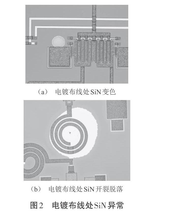
利用传统方法制作GaAs器件的过程中,会在芯片表面生成一定厚度的SiN(Silicon Nitride,氮化硅)介质层(总厚度300~500 nm),以阻挡潮气、离子沾污等因素对芯片的影响。在器件制作过程中,也发现了一些影响器件稳定性和可靠性的隐患。芯片表面金属镀层布线工艺经常出现应力集中点,导致该点氮化硅变色甚至开裂脱落,或者后续封装过程中受机械冲击时易产生微裂纹,严重影响芯片整体的可靠性[1-4]。
1 传统电镀布线工艺及问题
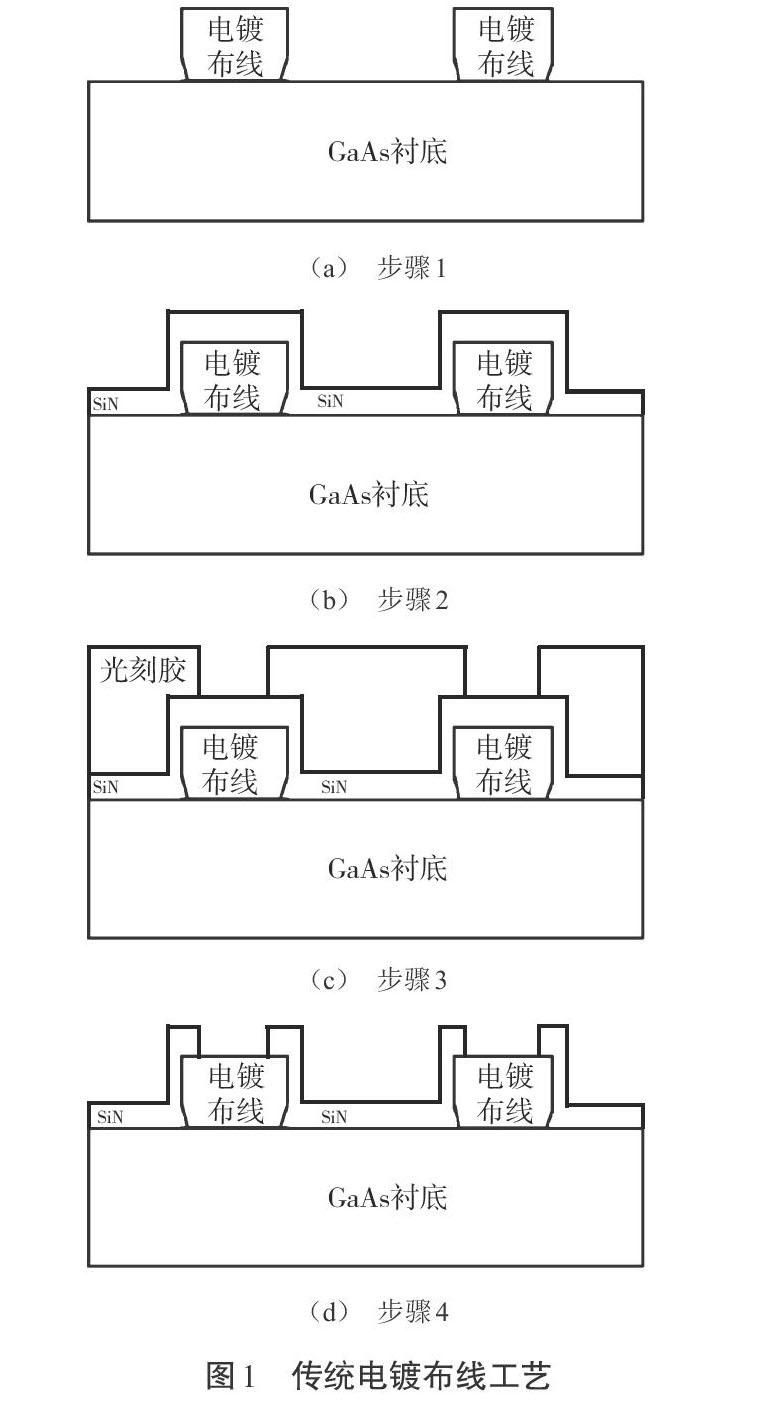
传统电镀布线工艺如图1所示。从图1可知,传统电镀布线工艺可分为四个步骤。……
