Localized electric-field-enhanced low-light detection by a 2D SnS visible-light photodetector*
2021-05-24HaoWen文豪LiXiong熊力CongbingTan谭丛兵KaiminZhu朱凯民YongTang唐勇JinbinWang王金斌andXiangliZhong钟向丽
Hao Wen(文豪), Li Xiong(熊力), Congbing Tan(谭丛兵), Kaimin Zhu(朱凯民), Yong Tang(唐勇),Jinbin Wang(王金斌), and Xiangli Zhong(钟向丽)
School of Materials Science and Engineering,Xiangtan University,Xiangtan 411105,Hunan,China
Keywords: two-dimensional SnS,photogating effect,low-light detection
1. Introduction
In the fields of video imaging and optical communications, visible-light detectors that can work under poor lighting conditions are urgently needed. Up until now, low-light signal detection has played an important role in space exploration, etc.[1,2]However, at present, commercial visible-light photodetectors, mainly based on Si, Ge and CdS,suffer from with high noise levels,which hinders their application in lowlight detection. The adjacent layers of two-dimensional (2D)layered materials are weakly bound by the van der Waals interaction, which gives them special structural and physical properties.[3,4]Their high carrier mobility, perfect switching characteristics, strong light interaction and ease of processing give 2D materials great potential for use in the fields of electronics and optoelectronics.[5–9]The photogating effect is a special phenomenon that exists in most photodetectors based on 2D materials.[10,11]Devices that work by the photogating effect usually obtain higher photoconductive gains(G)at low incident optical densities.[12–14]Thus, two-dimensional layered materials are one of the promising candidates for manufacturing high-performance low-light detectors.
In tin sulfide (SnS), one of the group IVA metal monochalcogenide semiconductors (MX, M =Ge, Sn; X =S, Se, Te), which is similar to puckered black phosphorous (BP),[15]one Sn atom bonds with three S atoms to form S–Sn layers with a van der Waals force present between them.[16]The SnS has an indirect bandgap of 1.07 eV and a direct bandgap of 1.3 eV, and therefore possesses a high light-absorption coefficient (α >104cm−1) in the visible spectrum.[17]Because it is stable in air, non-toxic,and earth-abundant, SnS has been seen as a suitable candidate for thin-film solar cells,[18,19]photocatalysis,[20]and photodetectors.[21–23]For example,Deng et al.[21]synthesized SnS nanoribbons in the solution phase and then fabricated a SnS-based photodetector for the first time; the photoconductivity gain(G)reached up to 2.3×10⁴when illuminated by a 532 nm laser at an optical density of 50 mW·cm−2. Zhou’s group[22]fabricated an ultrathin SnS nanobeltbased nearinfrared (NIR) photodetector; their device showed a photoresponsivity of 300 A·W−1under the illumination of 800 nm light at a density of 2.57 mW·cm−2, and a photocurrent transition time as fast as 43 ms.
In this work, highly crystalline 2D SnS nanosheets were prepared by a conventional physical vapor deposition (PVD)method. An 2D SnSbased two-terminal photodetector was constructed using ultraviolet photolithography. The device offers good lightsensing performance and cycling stability, and in particular,a high responsivity of 161 A·W−1and a high detectivity of 1.16×10⁹Jones when illuminated by a 450 nm laser at the fairly weak optical density of 2 mW·cm−2. Compared with other photodetectors in similar bands, our device shows some advantages in weak light conditions(Table 1).
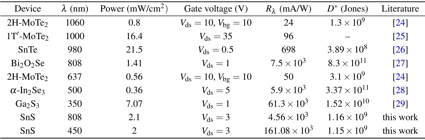
Table 1. Comparison of the photoelectric performance of our SnS photodetector versus other 2D materials.
2. Materials and methods
2.1. Growth and characterization of 2D SnS nanosheets
Two-dimensional SnS nanosheets were prepared using the physical vapor deposition (PVD) technique in a horizontal double-zone tube furnace (AnHui HeFei KeJing materials technology Co, Ltd.). For the growth process, 0.05 g of bulk SnS powder (99.5%, Alfa Aesar) in a quartz boat was used as the evaporation source and placed at the center of the hightemperature(HT)zone.Silicon substrates with a 300 nm-thick SiO2buffer layer were placed 15–20 cm away from the source in the low-temperature(LT)zone.Before heating commenced,the quartz tube was purged four times using high-purity Ar gas to drive off oxygen, then the HT zone and the LT zone were heated to 750°C and 550°C,respectively,at a speed of 20°C/min. When the HT zone reached 750°C,the temperature was maintained for 10 minutes in this area, ensuring the full evaporation of the SnS powder,and the temperature of LT zone was kept at 550°C at the same time. The Ar gas pressure in the quartz tube was fixed at 80 Torr with a flow rate of 70 standard cubic centimeters(sccm).
The morphology, size, and distribution of the synthesized 2D SnS nanosheets were characterized by an optical microscope (OM; Zeiss Primo Star) and field-emission scanning electron microscopy (FESEM; JSM-6700F). Powder Xray diffraction (XRD; Rigaku Ultima IV) was used to analyze the chemical composition, and high-resolution transmission electron microscopy(HRTEM;JEM 2100F)was carried out to confirm the single crystallinity of the samples. The TEM samples were prepared by the liquid-phase ultrasonic method. First, we put the SnS/SiO2/Si samples into a beaker which contained 10 mL ethanol,then the mixture was treated with ultrasonic oscillation for 20 minutes to exfoliate the SnS nanosheets from the SiO2/Si substrate, after which the SnS was suspended on the ethanol. Finally, the dispersion liquid was dropped onto a Cu grid and dried. UV-Vis diffuse reflectance spectroscopy (PerkinElmer 950) was used to measure the light-absorbing properties of SnS powder. The thickness of the nanosheets was measured by atomic force microscopy (AFM; Asylum Research MFP-3D Infinity). The collection of Raman spectra was carried out by a Renishaw inVia system with an excitation wavelength of 532 nm and a power of 500µW.The laser was focused on the top surface of a single SnS nanosheet.
2.2. Fabrication and characterization of the 2D SnS-based photodetector
Ultraviolet photolithography was applied to fabricate the 2D SnS-based two-terminal photodetector. Two Au–Ti(20 nm:10 nm) electrodes were deposited on an individual SnS nanosheet. Electrical measurements were carried out at room temperature using a semiconductor analyzer (Agilent B1500A) equipped with a four-channel probe station (EB).The photoresponse of the device was measured under 450 nm laser illumination.
3. Results and discussion
High-quality SnS nanosheets were synthesized in a double-zone tube furnace, as shown in Fig. 1(a). We found that lower temperatures in the deposition area facilitated largescale nanosheet growth,mainly by weakening the thermal motion of the Sn and S atoms. Therefore, when they reached the LT zone, they were more easily able to nucleate on the substrate.[30]In Fig.1(b),a typical optical image(center)and an SEM(bottom left)image of the SnS nanosheets on a mica substrate are clearly shown;the lateral dimensions of the SnS nanosheets range from 2 µm to 40 µm. Almost all of the nanosheets are near-rectangular in shape, and consistent with the shape of orthorhombic SnS crystals, as demonstrated in previous 2D SnS studies.[17,23,31]On the right side of Fig.1(b),EDS images of the nanosheet reveal the distributions of S and Sn elements within a single SnS nanosheet,indicating the uniformity of a single SnS nanosheet. The EDX spectrum in Fig. 1(c) further illustrates that the ratio of S and Sn atoms in a single nanosheet is 1:1, which proves the high purity of SnS.The Si elements originate from the silicon substrate.
To support the structural analysis of the SnS nanosheets,Raman spectra were obtained to provide molecular rotation and vibration information. According to previous reports,SnS has two major active modes, Agand B3g.[17,32]As illustrated in Fig. 1(d), three peaks located at 94.5 cm−1, 194.6 cm−1,and 219.0 cm−1belong to the Agmode, while the peak at 165.2 cm−1belongs to the B3gmode. These results confirm the pure orthorhombic phase of the synthesized SnS nanosheets. The AFM image in Fig.1(e)shows an individual SnS nanosheet with a height of 7.3 nm and a flat surface,corresponding to thirteen SnS monolayers. To further investigate the crystal structure of the sample,a TEM test was conducted.As shown in Figs. 1(f) and 1(g), the selected area electron diffraction(SAED)pattern shows sharp diffraction spots,and the HRTEM image shows that the lattice spacing is 0.34 nm,which is a good match for the (120) plane of the SnS. These results confirm the single-crystalline quality of the rectangular SnS nanosheets.

Fig. 1. (a) Schematic of the double-zone tube furnace used for 2D SnS growth, (b) optical image of large-scale SnS nanosheets with uniform shapes; lower left: SEM image of SnS nanosheets; upper right: S and Sn elemental mapping of a single SnS nanosheet; (c) EDX spectrum of an SnS nanosheet;(d)Raman spectrum of an SnS nanosheet at room temperature;(e)AFM images and height information of the sample;(f)SAED and(g)HRTEM pattern of the corresponding SnS nanosheet.
To study the photoelectric properties of SnS, measurements of the SnS powder were made by UV-Vis diffuse reflectance spectroscopy(DRS),as illustrated in Fig.2(a). The weak reflection at wavelengths of 400–900 nm indicates the strong light-absorbing properties of SnS in the visible light range. By adding a tangent line for the linear part of the reflection in Fig.2(a),we confirm that the edge of the SnS light absorption is located at about 1000 nm and close to an indirect bandgap of about 1.1 eV(1100 nm). The SnS-based photodetector was fabricated using a series of processes as described in the experimental section. A schematic of the structure of the device is visualized in Fig. 2(b), and figure 2(c) exhibits an optical image of the top surface. From the optical image,we can easily conclude that the SnS conductive channel length is 8µm. The I–V curves of the device under different optical laser powers are shown in Fig. 2(d), at a laser wavelength of 450 nm. When the incident optical power is increased from 0.5 to 44.3 mW,the photocurrent of the device increases from 405 nA to 5.048µA,showing an obvious response to 450 nm blue light. The blue to red lines correspond to dark current and photocurrent at different optical powers,respectively. It is noteworthy that Fig. 3(a) shows the dark current of the photodetector at bias voltages of −3 to 3 V, for which the zero dark current area lies in a low voltage range, indicating an energy gap between the SnS nanosheet and the Ti/Au electrodes. Nearly symmetrical I–V characteristic curves in the positive(V >0)and negative areas(V <0)illustrate the nonrectifying effect of the metal-semiconductor junction.According to previous research,P-type semiconductors made of SnS have a work function of 4.2 eV, smaller than that of titanium(4.33 eV), and the hole concentration in solution-phase synthesized SnS nanoribbons is larger than 1019cm−3. A dark current larger than 100 nA at a bias voltage of 1 V also confirms the huge hole concentration in SnS.The items mentioned above indicate an ohmic contact between the SnS nanosheet and the Ti–Au electrodes. The investigation into the photodetector was performed at room temperature,and the room was kept dark during the test.[10,33–35]

Fig. 2. (a) UV-Vis reflection spectrum of SnS; (b) schematic of 2D twoterminal photodetector; (c) optical image of the two-terminal structure;(d)I–V curves of device under blue light at 450 nm with different powers.The measurements were carried out at room temperature.
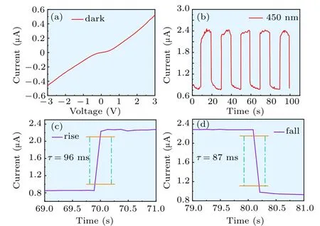
Fig. 3. (a) Dark current of device with bias voltage sweeps from −3 to 3 V.The laser wavelength is 450 nm. (b)The stable switching behavior of the device under 450 nm light illumination with a 3 V bias voltage; (c)the response and(d)recovery time of the device under visible light at 450 nm.
Next,we tested the cycling performance of the device,as shown in Fig. 3(b). The current of the device rose to a high value in the light absorption period (with the laser on), but remained at a low value in the dark(with the laser off). In detail,the photodetector was illuminated by a 450 nm laser with an optical density of 47 mW·cm−2;the laser was switched on and off repeatedly at 10 s intervals at a bias voltage of V. As shown, the device current in the laser’s ‘off’ state was below 1µA while it was larger than 2.2µA in the laser’s‘on’state,making a good identification of photoswitching performance of device. In particular, there is no obvious reduction in the photocurrent during the testing period. In addition,the photoswitching rate of the device is vital for practical applications.To our knowledge,the response and recovery time τ is calculated as

in which τrrefers to the time required for the current to rise from 10%of the maximum photocurrent to 90%,while,on the contrary,τfdenotes the time required for the current to decay from 90%of the maximum photocurrent to 10%.[36–39]The response and recovery processes of the device have been investigated and the results are shown in Figs.3(c)and 3(d), from which τrand τfare deduced to be 96 ms and 87 ms, respectively. In summary,the SnS nanosheetbased photodetector exhibits an excellent photoresponse and stable photoswitching.These features benefit from the high crystalline quality of the nanosheets and the large specific surface areas,which help to bring about fast photo-excited carrier diffusion.

According to previous reports,[36]the dependence of the photocurrent on the incident optical density fits the law Iph∝. Significantly, there are several key parameters used to assess the properties of photodetectors.First,the photoresponsivity(Rλ)is used to estimate the photoelectric switching ability,as calculated by the formula where the photocurrent, ΔI=Iphoto−Idark, while Pλrefers to the power density of the incident light, and S is the effective illuminated area of the device. Figure 2(c) shows that the channel area of the SnS photodetector is about 80 µm2.To be specific, the area of the incident light spot reaches 24 mm2, which is much larger than the channel’s surface area, so here, S=80µm2. Taking the 0.5 mW incident light power and 3 V bias voltage into account,ΔI=0.403µA andS=2.5×10⁻⁶mW,thus Rλis calculated to be 161.08 A/W.The external quantum efficiency (EQE) is obtained using the following equation:where h is Planck’s constant,c is the velocity of light,λ is the wavelength of the light used for excitation,and e is the electron charge. After calculation,the EQE reaches up to a surprising 4.45×10⁴%, which exceeds that of many other IV–VI group compounds reported previously.The detectivity(D*),an index used to estimate the sensitivity of light signals,is expressed as
According to this formula, the D*of the device is calculated to be 1.15×10⁹Jones. Figure 4(a) presents Rλand EQE versus the optical power density. When the incident optical power density rises from 2 to 177 mW·cm−2, both Rλand EQE clearly decrease. Figure 4(b) shows Rλand D*versus power density; the detectivity of the device also drops from 1.15×10⁹to 1.63×10⁸Jones with increasing power density under light illumination at 450 nm. We also measured the photoresponse performance of the device at a wavelength of 808 nm (in Fig. 5). Under light at 2.1 mW/cm2, Rλis 45.6 A/W, which is lower than at a wavelength of 450 nm.At 808 nm,the Rλ,EQE and D*also show a tendency to decrease rapidly as the optical power increases. Zheng et al.[40]reported that the photoresponsivity of a SnS nanowire photodetector reached its maximum at 700 nm, and when the wavelength was greater than 800 nm, the photoresponsivity decreased rapidly. Their result is consistent with our experimental observations.
At low optical densities, the high optical responsiveness of SnS photodetectors may be caused by the photogating effect. Figures 4(c), 4(d)and 4(e)show schematic diagrams of carrier distribution in a semiconductor channel in the dark and under different illuminations. The photogating effect of the device is due to two mechanisms: (i)In two-dimensional SnS photodetectors,the local electric field caused by nanoparticles or defects traps some of the carriers and acts as a gate.[2,41–44]Huang et al.[45]and Liu et al.[46]proposed that SnS defects may be caused by S vacancies. Under light conditions, photogenerated electron-hole pairs are generated in the channel.Because of the structural defects in SnS nanosheets or disorder at the interface, band tail states inevitably appear in the conduction and valence bands.[24]When the photodetector is illuminated,the electron-hole pairs excited by the light are firstly separated by an external bias voltage, and then the electrons are likely to be trapped in a localized state. They can be regarded as partial gates. Because the photocurrent generated is determined by Iphoto=gm×ΔVg(Iphotois the photocurrent,gmis the transconductance,ΔVgis the gate voltage),the presence of local gates increases the photoresponse.[41](ii)In addition,one type of carrier is captured, which extends the life of another type of carrier. Since the total charge remains neutral,then Δp=Δn+nt(Δp and Δn are the densities of photogenerated holes and electrons,respectively,ntis the trapped electron carrier concentration),and the additional photoconductivity can be expressed as follows:

where µnand µpstand for the mobilities of electrons and holes, respectively. Obviously, the separation effect due to local states increases the photoconductivity.[24]Since ntare limited by the number of defects,the photogenerated electronhole pairs cannot effectively be separated when the local state is fully occupied. Therefore,continuing to increase the optical power will shorten the carrier lifetime,resulting in a decrease in Rλ,EQE and D*.

Fig. 4. (a) Induced Rλ and EQE, (b) Rλ and D* properties of the device for a range of optical power densities; (c) band alignment of the SnS channel connected by two Ti–Au electrodes under external bias in the dark. The blue dotted circles represent the local state in the conduction band edge;(d)the local state captures the photogenerated electrons,and the electrons are trapped at the edge of the band as a local gate;(e)when the local state is full.
We further analyzed the dependence of photocurrent on optical power.As shown in Fig.6,under different voltages,the relationship between the photocurrent and the optical power in the device is nonlinear. This phenomenon may be caused by the combination of two mechanisms: the photoconductive effect and photogating effect.[24]The process of the photocurrent change can be divided into three stages: (i)When the optical power is fairly weak,the photogating effect plays a major role; qµpnt(the gain in photoconductivity caused by defecttrapped carriers)increases with the optical power, so that Δσ and the photocurrent increase rapidly;(ii)With an increase of the optical power,more carriers are generated in the channel.Defects that are filled reduce the separation effect of electronhole pairs, so that the photocurrent growth slows down. But at the same time,the defecttrapped carriers form a local gate,making the photocurrent increase; (iii) Both qµpntand ΔVgreach a maximum when the defects are full; an increase of the optical power will lead to a further reduction in the photocurrent growth rate.At this stage,the photocurrent is mainly produced by the photoconductivity effect.
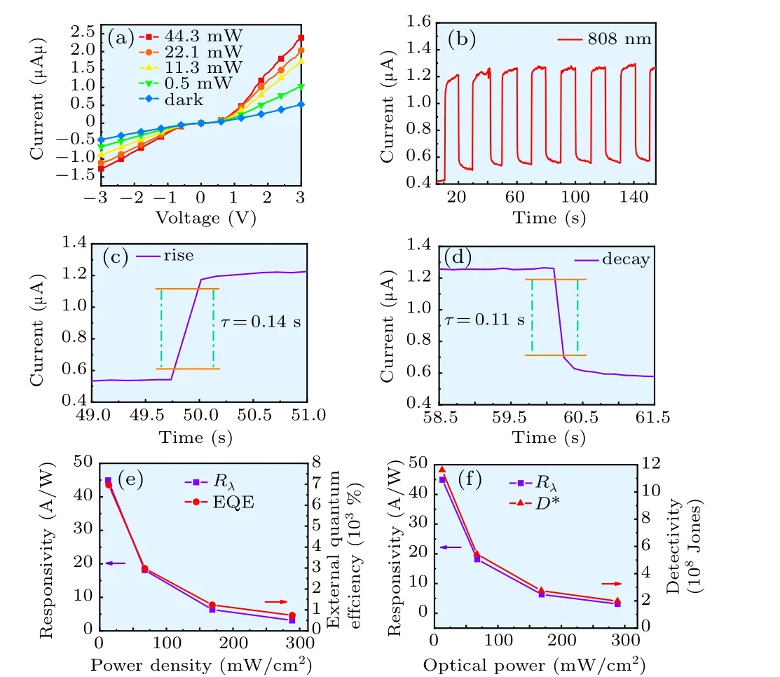
Fig. 5. (a) I–V curve of the device under blue light at 808 nm at different powers;the measurements are carried out at room temperature. (b)The stable switching behavior of the device under 808 nm light illumination at a 3 V bias voltage;(c)the response and(d)recovery times of the device under visible light at 808 nm; (e)the induced Rλ and EQE,(f)Rλ and D* properties of the device for varying optical power densities at 808 nm.
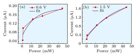
Fig.6. (a)and(b)the relationship between photocurrent and optical power at different voltages,for a wavelength of 450 nm.
4. Conclusion
In summary,we fabricated a 2D SnS-based two-terminal photodetector. At a low optical density of 2 mW·cm−2,the photodetector obtained a high responsivity (Rλ) of 161.08 A·W−1, while the external quantum efficiency (EQE)and detectivity (D*) reached up to 4.45×10⁴% and 1.15×10⁹Jones, respectively. These results show that the twodimensional SnS has the potential to be applied in low-light detection. When the optical power density increases,Rλ,EQE and D*all show a downward trend. This phenomenon is explained by the photogating effect. The defects in the SnS nanosheets or the local electric field formed in the interface can trap electrons and extend the life of holes. When the optical power density increases,the local states are filled,and the local electric fields have a reduced effect on electron-hole pair separation,resulting in a shortened carrier lifetime.Therefore,Rλ,EQE and D*show a decreasing trend with an increase in optical power density.
猜你喜欢
杂志排行

Chinese Physics B的其它文章
- Corrosion behavior of high-level waste container materials Ti and Ti–Pd alloy under long-term gamma irradiation in Beishan groundwater*
- Degradation of β-Ga2O3 Schottky barrier diode under swift heavy ion irradiation*
- Influence of temperature and alloying elements on the threshold displacement energies in concentrated Ni–Fe–Cr alloys*
- Cathodic shift of onset potential on TiO2 nanorod arrays with significantly enhanced visible light photoactivity via nitrogen/cobalt co-implantation*
- Review on ionization and quenching mechanisms of Trichel pulse*
- Thermally induced band hybridization in bilayer-bilayer MoS2/WS2 heterostructure∗