Ferroelectric effect and equivalent polarization charge model of PbZr0.2Ti0.8O3 on AlGaN/GaN MIS-HEMT*
2021-05-24YaoPengZhao赵垚澎ChongWang王冲XueFengZheng郑雪峰XiaoHuaMa马晓华AngLi李昂KaiLiu刘凯YunLongHe何云龙XiaoLiLu陆小力andYueHao郝跃
Yao-Peng Zhao(赵垚澎), Chong Wang(王冲), Xue-Feng Zheng(郑雪峰), Xiao-Hua Ma(马晓华),Ang Li(李昂), Kai Liu(刘凯), Yun-Long He(何云龙), Xiao-Li Lu(陆小力) and Yue Hao(郝跃)
Key Laboratory of Wide Band-Gap Semiconductor Materials and Devices,School of Microelectronics,Xidian University,Xi’an 710071,China
Keywords: PZT,AlGaN/GaN,MIS-HEMT,equivalent polarization charge model(EPCM)
1. Introduction
AlGaN/GaN high electron mobility transistors(HEMTs)have a two-dimensional electron gas (2DEG) with high electron density and mobility in the channel because of the spontaneous polarization and piezoelectric polarization,[1–4]and they are well suited for applications in power switching devices.[5–8]The integration of ferroelectric materials and Al-GaN/GaN has attracted much attention because of exhibiting some unusual characteristics.[9,10]Recently, some ferroelectrics have been integrated with GaN-based HEMTs, such as PbZrxTi1−xO3(PZT). The polarization of PZT is several orders of magnitude larger than that of AlGaN/GaN and is variable and reversible when different electric intensities are applied.[11]Moreover, the polarization of PZT can modulate the 2DEG density of AlGaN/GaN heterojunctions,and this has been reported in some studies.[11,12]
Gate dielectric material is of vital importance for MISHEMTs.[13,14]Different from the traditional oxide and nitride,ferroelectric materials have strong polarization effect, resulting in the modulation of the 2DEG density and the current density.[15]The nonlinear polarization characteristics of ferroelectric materials make it possible to modulate the 2DEG density under the gate without sacrificing the gate-control ability.[15]However,few articles have reported the specific calculation model of the PZT gate dielectric for the AlGaN/GaN MIS-HEMTs.
In this paper, AlGaN/GaN MIS-HEMTs with Pb(Zr,Ti)O3(PZT)ferroelectric gate dielectric are fabricated.The PZT gate dielectric is grown by pulsed laser deposition(PLD).A theoretical calculation model of polarization charge is proposed. Moreover, the DC and pulse characteristics are analyzed.
2. Device fabrication
The AlGaN/GaN heterojunction structure used in this paper was grown on the sapphire substrate by the metal organic chemical vapor deposition(MOCVD)method.The wafer consists of an AlN nucleation layer, an AlGaN gradient layer that the Al percent is from 8% to 0, a 1-µm-thick undoped GaN layer, a 160-nm-thick undoped GaN channel, and a 25-nm-thick undoped Al0.25Ga0.75N barrier layer. Room temperature Hall measurements of the epi-wafer yield an electron sheet density of 9.2×1012cm−2and an electron mobility of 1986 cm2/V·s.
The mesa area was formed by using BCl3/Cl2plasma etching in an inductively coupled plasma (ICP) system followed by the drain/source Ohmic contact formation using Ti/Al/Ni/Au(30 nm/180 nm/40 nm/60 nm)annealed at 840°C for 30 s. A 60-nm-thick Si3N4layer was deposited on the surface by the plasma enhanced chemical vapor deposition(PECVD), and the Si3N4of the gate area was removed by CF4/O2plasma etching. Then, the PZT dielectric layer was deposited by pulsed laser deposition(PLD)with the thickness of 30 nm. Then, Ni/Au E-beam evaporation and lift off were carried out to form the gate electrode. The Lg,Lgd,and Ldsof the devices are 1.0µm,3.5µm,and 7.0µm,respectively. The Wgof the devices are 50 µm. Figure 1 shows the schematic cross-sectional structure of the gate recessed MIS-HEMT.Figure 2 shows the photomicrograph of the MIS-HEMT.The parameters of the devices were measured by Keithley 4200.

Fig. 1. The schematic cross-sectional structure of PZT AlGaN/GaN MISHEMT.
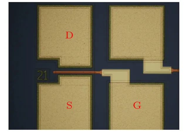
Fig.2. The photomicrograph of the MIS-HEMT device.
3. Results and discussion
Figure 3(a) shows the transfer characteristics of the four sweeping speeds of gate voltage. The maximum drain current density reaches 800 mA/mm with the drain voltage of 10 V when the gate voltage sweeping speed is 2 V/s. The current density decreases to 450 mA/mm when the sweeping speed is up to 20 V/s. For the same device, as the change of polarization charge takes time, the amount of polarization charges in PZT is different at different sweeping speeds and different amount of polarization charge leads to different current densities. The peak trans-conductance decreases from 122 mS/mm to 40 mS/mm when the scanning speed is 2 V/s and 20 V/s,respectively. The trans-conductance decreases due to the depletion of electrons in the channel by the polarization charge.When the sweeping speed is 20 V/s, the polarization charge cannot keep pace with the change of the gate voltage, which results in the decrease of the current density. The calculation model of polarization charge will be presented in the following part.
Figure 3(b)shows the transfer curve in logarithmic coordinates. Excellent off-state performance was achieved with a low leakage current of about 10−10A/mm.The threshold voltage(Vth)in this paper is defined as the gate bias when the drain current reaches 1 mA/mm. The Vthincreases from −12.2 V to−8 V when the scanning speed is 2 V/s and 20 V/s, respectively.The change of polarization charge can modulate the Vth,and the modulation range is up to 4.2 V,which is an effective method to realize the enhancement-mode devices.
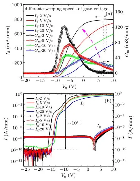
Fig. 3. Transfer characteristic curves of different sweeping speeds of gate voltage(a)conventional coordinates and(b)logarithmic coordinates.
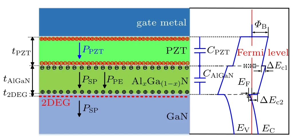
Fig.4. Polarization charge diagram and energy band diagram of PZT MISHEMT.
The polarization charges and energy band of MIS-HEMT are shown in Fig.4. In AlGaN/GaN heterojunction,electrons will be confined at the interface because of spontaneous polarization and piezoelectric polarization. To calculate the amount of the polarization-induced sheet charge density σ at the Al-GaN/GaN interface, we use the following set of linear interpolations between the physical properties of GaN and AlN[16](the x is the Al-content of the AlxGa1−xN barrier):

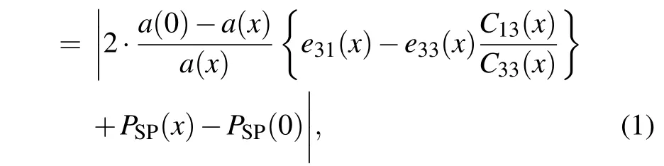
where a(x) is lattice constant, C13(x) and C33(x) are elastic constants,e33(x)and e31(x)are piezoelectric constants,Psp(x)is spontaneous polarization. The specific calculation methods of these parameters are shown in Ref. [16]. When x is 0.25,σ(x)is 0.022 C/m2.
The distance between PZT polarization charge and 2DEG is large compared with the σ of the AlGaN/GaN interface.The force between the polarization charge and the electrons in the channel is inversely proportional to the distance. We propose an equivalent polarized charge model(EPCM)with the calculation method as given in Eq. (2), it can be used to calculate the effect of both the PZT and AlGaN polarization charges on the 2DEG.σ′(x)is the equivalent polarization charge.
where tAlGaNis the thickness of the barrier layer, tPZTis the thickness of the PZT layer, t2DEGis the distance between 2DEG and the polarization charge of the AlGaN surface. According to the C–V curve and the distribution of 2DEG,t2DEGis taken as 1 nm.Equation(2)can be simplified as Eq.(3)after substituting the values of each thickness into the equation.

According to Eq.(3),it can be concluded that the polarization charge of PZT must be an order of magnitude larger than that of AlGaN in order to have a significant effect on the device performance. Capacitor of PZT and AlGaN are connected in series. The 2DEG concentration formula of MIS-HEMTs can be obtained from[17]
where φB(x)is the Schottky-barrier height,EFis the difference between Fermi level and GaN conduction band edge level,and ΔEC1and ΔEC2is the conduction band discontinuity between PZT and AlGaN,and AlGaN and GaN.
Figure 5(a) shows the trend of polarization charge and electron concentration. With the increase of PZT polarization charge,the equivalent polarization charge and the electron concentration increase linearly. When the polarization charge of PZT reaches 0.5 C/m2, both of the equivalent polarization charge and the electron concentration increase by 48.6%. The polarization charge of PZT has a great ability to control the channel electron concentration. Figure 5(b)shows the trend of polarization charge of PZT with different gate voltages. According to the MFM structure in the reference,[11]the polarization charge of PZT has hysteresis in the process of gate voltage sweep back. The hysteresis characteristics of PZT are different with different sweeping speeds.When the speed of voltage scanning is faster,the hysteresis of the curve is larger because of the delay of the change of the planned charge. Therefore,in the process of voltage increasing,when the voltage sweeping speed is faster, the corresponding polarization charge is smaller.
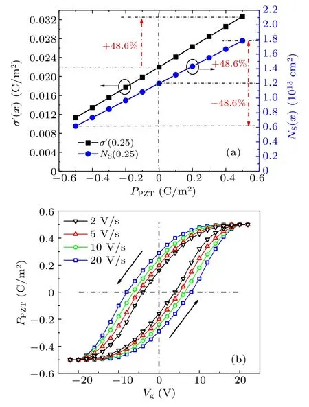
Fig. 5. (a) The trend of polarization charge and electron concentration and(b)the trend of polarization charge of PZT with different gate voltages.
For the HEMT devices, the current between source and drain(IDS)can be calculated by

where W is the gate width, v(x) is the velocity of the electrons in the channel. As the barrier layer is not etched, the electron velocity is proportional to the electron mobility, and the electron mobility remains unchanged. The IDSis mainly determined by the NS(x).
Capacitors of PZT and AlGaN are connected in series.Assuming that the 2DEG in the channel is totally depleted at Vth,the Vthcan be expressed as[17]

where εPZTis dielectric constant of PZT.
According to the above formula and experimental results,the experimental and theoretical results of IDSand Vthcan be obtained.Figure 6 shows that the theoretical values are in good agreement with the experimental results.The EPCM proposed in the present paper can guide the design of the PZT MISHEMT.
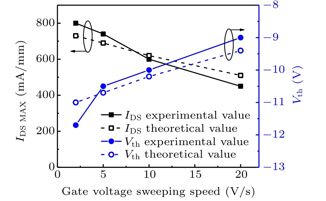
Fig.6. Experimental and theoretical values of IDMAX and Vth for the MISHEMT.
Figure 7 shows the change of the transfer characteristics with different gate voltage stresses. According to the results shown in Fig. 3, the transfer characteristics were tested with the sweeping speed of 2 V/s. The gate voltages were swept from −20 V to 10 V and the maximum gate voltage is equal to the stress voltage. This avoids the sweeping voltage having an influence on the stress effect. As shown in Fig.7(a),the Vthincreases from −11.2 V to −7.1 V after applying 10-V gate voltage for 210 s. The Vthhas a positive shift with an increase time in the stress–gate voltage. Moreover,the Vthchanges little from 150 s to 210 s, indicating that the modulation of polarization charge has reached the limit. The polarization of PZT in PZT/AlGaN/GaN HEMT is enhanced with an increase time and this means that more negative polarization charges of PZT are switched in the PZT/AlGaN interface. Therefore,the two-dimensional electron gas density at the channel decreases,and Vthhas a positive shift. Figure 7(b)shows that the Vthdecreases from −7 V to −11 V after applying −20-V gate voltage for 210 s. The same principle as mentioned above is due to more positive polarization charges of PZT being switched in the PZT/AlGaN interface.

Fig.7. (a)Transfer characteristics of 10-V gate stress for different time and(b)transfer characteristics of −20-V gate stress for different time.
Figure 8(a) shows the comparison of output characteristics before and after the gate-voltage stress. After a gatevoltage stress of 10 V for 120 s, the maximum output current density only decreased from 781 mA/mm to 779 mA/mm and the current density decreased from 518 mA/mm to 424 mA/mm when the gate voltage is 10 V and −2 V,respectively. After the stress is applied, the Vthis positively biased,which leads to the decrease of the output current at the same gate voltage. The on resistance(Ron)also remains unchanged before and after the stress,which is 4.6 Ω·mm.This shows that the gate voltage can modulate Vthof the device. When testing the output current curves,the drain voltage increases from 0 V to 10 V by keeping the gate voltage bias unchanged. Therefore,when the gate voltage is stable,the polarization charge is fixed and the output characteristics of the device remain stable.
Figure 8(b)shows a dual-pulse current collapse test performed on the device.In the test,the pulse width is 5×10⁻⁷s,with 1-ms period and 1.5×10⁻⁷-s rise time and the decline time.[18]The current collapse test selects two static operating points,the(Vgs,Vds)=(0,0)state and the(Vgs,Vds)=(−8,10)state. According to the measurement, the current collapse of the MIS-HEMT is 5.2%. Because the voltage change in the current collapse test is at the microsecond level and the change of polarization charge takes many seconds, the polarization charge has no time to follow the change of the gate voltage.Therefore,the current collapse of the device is very small and the current collapse characteristic is very stable.
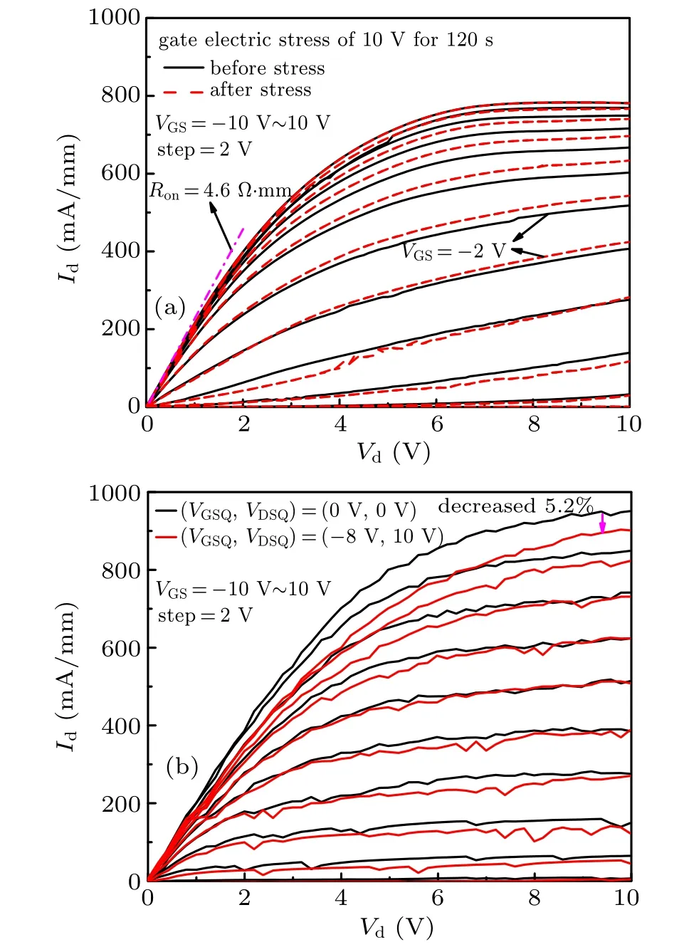
Fig.8. (a)Output current curves of before and after gate stress for 120 s and(b)pulse output current curves of the devices.
The multi-frequency C–V characteristics are shown in Fig.9. The C–V curves of different frequencies are basically coincident,and the maximum value of dispersion is only 0.3 V.At the same time,the C–V curves is swept back and the maximum hysteresis is 0.5 V.According to the results of the C–V curves,the Vthis stable when the polarization charge is fixed.In the C–V test, the frequencies are from 10 kHz to 1 MHz and the corresponding time is from 1 µs to 100 µs, respectively. The polarization charge is also difficult to keep up with the changing speed, so the polarization charge is also stable.Therefore,the Vthcan be adjusted according to the modulation of polarization charge.

Fig.9. Multifrequency C–V curves of PZT MIS-HEMT.
4. Conclusion
The PbZr0.2Ti0.8O3AlGaN/GaN metal–insulator–semiconductor high electron mobility transistors (MISHEMT) is fabricated on the sapphire substrate. The ferroelectric effect is shown in the transfer characteristics. The amount of polarization charges in PZT are different at different sweeping voltage speeds. An equivalent polarization charge model is proposed for calculating the concentration of 2DEG.The threshold voltage(Vth)and output current density(IDS) can be obtained by the theoretical model. The theoretical values are in good agreement with the experimental results and the model proposed can guide the design of the PZT MISHEMT. The polarization charges of PZT can be modulated by different gate-voltage stresses. So the Vthhave a regulation range of 4.0 V.The polarization charge changes after the stress of gate voltage for several seconds. When the gate voltage is stable or changes at high frequency,the output characteristics and the current collapse of the device remain stable.
猜你喜欢
杂志排行

Chinese Physics B的其它文章
- Corrosion behavior of high-level waste container materials Ti and Ti–Pd alloy under long-term gamma irradiation in Beishan groundwater*
- Degradation of β-Ga2O3 Schottky barrier diode under swift heavy ion irradiation*
- Influence of temperature and alloying elements on the threshold displacement energies in concentrated Ni–Fe–Cr alloys*
- Cathodic shift of onset potential on TiO2 nanorod arrays with significantly enhanced visible light photoactivity via nitrogen/cobalt co-implantation*
- Review on ionization and quenching mechanisms of Trichel pulse*
- Thermally induced band hybridization in bilayer-bilayer MoS2/WS2 heterostructure∗