Combined effects of carrier scattering and Coulomb screening on photoluminescence in InGaN/GaN quantum well structure with high In content∗
2021-05-06RuiLi李睿MingShengXu徐明升PengWang汪鹏ChengXinWang王成新ShangDaQu屈尚达KaiJuShi时凯居YeHuiWei魏烨辉XianGangXu徐现刚andZiWuJi冀子武
Rui Li(李睿), Ming-Sheng Xu(徐明升), Peng Wang(汪鹏), Cheng-Xin Wang(王成新),Shang-Da Qu(屈尚达), Kai-Ju Shi(时凯居), Ye-Hui Wei(魏烨辉),Xian-Gang Xu(徐现刚), and Zi-Wu Ji(冀子武),†
1School of Microelectronics,Shandong University,Jinan 250100,China
2Shandong Inspur Huaguang Optoelectronics Co.,Ltd.,Weifang 261061,China
3State Key Laboratory of Crystal Materials,Shandong University,Jinan 250100,China
Keywords: photoluminescence,carrier localization effect,internal quantum efficiency,growth temperature
1. Introduction
Much attention has been paid to white light-emitting diodes (WLEDs) for solid-state lighting applications due to their excellent brightness, low power consumption, long lifetime, and environmental friendliness.[1–3]Generally, white light emission results from the use of phosphor to transform part of emissions of blue LEDs to the yellow–green spectral range. The transformation is related to an energy loss termed Stokes’ loss, which is on the order of 25% and thus restricts the highest attainable phosphor-converted WLED efficiency to much less than 100%;[4,5]however, in principle, one can avoid the loss through the use of phosphor-free monolithic WLEDs, which are integrated by blue, green, and even red long-wavelength InGaN-based LEDs, since the nitride system can cover the entire spectral region of the emitted light from near-ultraviolet to near-infrared by adjusting the composition of InGaN alloy.[6,7]Therefore, InGaN-based LEDs are a promising candidate for realizing the phosphor-free monolithic WLEDs operated at a high efficiency.
Currently,InGaN/GaN multiple quantum wells(MQWs)-based blue LEDs with low In content have been found to have a high internal quantum efficiency (IQE) of about 90%,[8,9]however, by contrast, the IQE for the InGaN/GaN MQWsbased long-wavelength (e.g., yellow–green) LEDs with high In content is still much lower.[10–12]Several factors are responsible for the deterioration of emission efficiency.First,because of the low InN dissociation temperature, the high-In-content InGaN must be grown at low temperatures:[13]however,unfortunately,besides an increased density of structural defects[14]and incorporation of impurities,[15]the use of a low growth temperature for the InGaN well layers can result in more numerous composition fluctuation-induced point defects[16–18]and a stronger well/barrier lattice mismatch-induced quantumconfined Stark effect(QCSE)in the MQWs on account of the high In content.[19]Nevertheless,it has also been reported that in such InGaN/GaN MQW structures with a high-In-contentinduced compositional fluctuation, the In-rich regions in the InGaN well layers, acting as localization centers with deep potential levels, can restrict the outflow of carriers to nonradiative recombination center around, thus improving the emission efficiencies of the MQW structures.[20,21]In addition,some studies have shown that for a series of InGaN/GaN MQW LEDs with similar structures but different growth conditions, although those members in the set have almost the same In content, their localization effects are different as reported in Refs.[22,23]. These reports show that the emission mechanisms of the InGaN/GaN MQW structures, especially those of the InGaN/GaN MQW structures with lower growthtemperatures used for formation of their InGaN well layers,are diverse,and a comprehensive investigation is thus deemed necessary.
In the present work, two green InGaN/GaN MQW samples with different growth temperatures of InGaN well layers are grown. To facilitate the incorporation of In into the MQWs and improve the emission efficiency of the MQWs,an underlying superlattice layer is introduced into both samples for releasing the strain in the MQW region.[24–26]The effects of growth temperature on the emission mechanism in such samples are investigated by measuring the dependence of photoluminescence(PL)spectra on temperature and excitation power.
2. Experiment
Two green InGaN/GaN MQW samples(S1 and S2)under study were grown on (0001)-oriented sapphire substrates via metal-organic chemical vapor deposition (MOCVD). During epitaxial growth,trimethylgallium(TMGa),ammonia(NH3),trimethylindium (TMIn), and silane (SiH4) were separately used as the precursors of Ga, N, In, and Si. The epitaxial structure for each of both samples includes a GaN buffer layer (25-nm thick), an undoped GaN layer (4-µm thick),an Si-doped n-type GaN layer (3-µm thick), five periods of In0.05Ga0.95N/GaN (1 nm/5 nm) forming a strain relief layer(SRL),and ten periods of InGaN/GaN(3 nm/17 nm)forming the MQW active region, in turn. For better comparison, the growth parameters of the two samples are the same except the growth temperature of InGaN well layers in the active region,which is 745◦C for S1 and 730◦C for S2.
Temperature and excitation-power-dependent PL were measured by placing samples on a Cu cold-stage in a closedcycle He cryostat at temperatures ranging from 6 K to 330 K,and a semiconductor laser (405-nm cw) with a spot size of about 200µm and an operating range of 0.001 mW to 75 mW was used as an excitation source. An iHR320 monochromator(Jobin-Yvon) and a thermoelectrically cooled Synapse CCD detector were used to scatter and detect PL signals, respectively.
3. Results and discussion
Figure 1 shows the typical 5-mW PL spectra of samples S1 and S2 detected at 6 K and 300 K,respectively, where all PL spectra exhibit one InGaN-related main PL peak at around 2.35 eV.Two weak peaks denoted as 1LO and 2LO at 6 K for both the samples are phonon replicas of the main PL peak. In order to estimate the peak position and linewidth of the main PL peak,the spectra are deconvoluted by multi-peak gaussian fitting.[21]Additionally,it is also found from Fig.1 that comparison between scenarios of samples S1 and S2 shows that the main PL peak of S2 has a lower energy and a slightly larger linewidth at all measured temperatures,and the integrated PL intensity shows a more significant reduction as the temperature increases from 6 K to 300 K.To further investigate the effects of growth temperature of the InGaN well layers on the emission mechanism of the InGaN/GaN MQWs,both the temperature and excitation-power-dependent PL spectra for the two samples will be investigated.
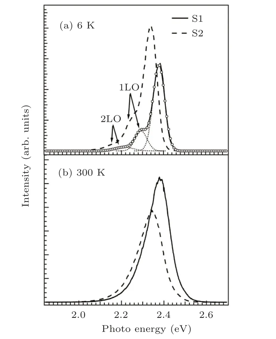
Fig.1.The 5-mW PL spectra of S1 and S2 at(a)6 K and(b)300 K,with two observed weak shoulder peaks(1LO and 2LO)at 6 K belonging to phonon replicas originating from the main peak, thin dotted lines denoting fitted Gaussion peaks of profile of S1 at 6 K,and empty circles referring to their sum.
Figure 2 shows the dependence of the PL peak energy and linewidth on excitation power for these two samples measured in a range of 0.001 mW–75 mW at 6 K. As seen from Fig.2, when the excitation power rises from 0.001 mW to about 0.02 mW, the peak energy remains almost unchanged while the linewidth narrows in a monotonic manner for each of the two samples. This behavior can be explained as follows: with the increase of excitation power in the initial range below about 0.02 mW, the increased free carriers in the In-GaN matrix can weaken the QCSE in the MQWs, resulting in an increase in peak energy accompanied by a decrease in linewidth; meanwhile, the increased localized carriers in the localized centers will enhance the carrier scattering effect,which causes the localized carriers to transfer from the highenergy localized centers to the low-energy localized centers by tunneling, resulting in a decrease in peak energy accompanied by a decrease in linewidth.[26–29]That is, the above MQW-related emission processes for both samples should be dominated simultaneously by the carrier scattering effect and the Coulomb screening effect of QCSE in the initial excitation power range. Nevertheless, by comparison, it is found from Fig.2 that the behaviour of the excitation-power-dependent linewidth narrowing is more significant for S2 than for S1,indicating that both the carrier scattering effect and the Coulomb screening effect in the process should be stronger for S2 than for S1. Next, when the excitation power further increases above about 0.02 mW,the peak energy values for both samples increase monotonically up to 75 mW,but the difference is that the linewidth of S1 significantly narrows below 10 mW due to the Coulomb screening effect, and then markedly broadens because of the filling effect of the high-energy localized states;in contrast,the linewidth of S2 slightly broadens below 0.1 mW due to the filling effect of the low-energy localized states,and then significantly narrows because of the more significant Coulomb screening effect.

Fig.2. Excitation-power-dependent peak energy and full-width at halfmaximum(FWHM)for(a)S1 and(b)S2 measured at 6 K.
The above results obtained from Figs. 1 and 2 suggest that S2 should have a higher In content in the MQW than S1 due to the lower growth temperature, and thus causing a more significant component fluctuation-induced potential fluctuation and a stronger well/barrier lattice mismatch-induced QCSE for S2,which eventually results in the aforementioned stronger excitation-power-dependent carrier scattering effect and Coulomb screening effect(Fig.2),respectively.
Figure 3 shows the excitation-power-dependent PL peak energy and linewidth of the two samples in a range of 0.001 mW–75 mW at 300 K. With the excitation power increasing, the PL peak energy and linewidth for each of the two samples exhibit an excitation-power-dependent approximately “V-shape” (decreasing-increasing) and an approximately “N-shape” (broadening-narrowing-broadening), respectively. These behaviors are often observed in similar InGaN/GaN-based structures,[21,27]and can be explained as follows. Under the 300-K high temperature measuring conditions, the defect-related non-radiative centers are thermally activated,with excitation power increasing in the initial excitation power range below a critical value(Pc),the non-radiative recombination dominates the emission process in the MQW,thus leading the peak energy to decrease and the linewidth to broaden as shown in Fig.3. Here,Pcis about 0.05 mW for S1 and about 0.2 mW for S2. In the case for the excitation power higher than Pc, as an increasing excitation power makes the non-radiative centers saturated,the Coulomb screening of the QCSE followed by the band-filling of high-energy localized states dominates the emission process of the MQWs for both samples. Moreover, it can also be seen from Fig.3 that the excitation-power-dependent behaviors of the peak energy and linewidth in the initial non-radiative recombination process and in the subsequent Coulomb screening process, are more significant for S2 than for S1. These results,together with the larger Pc(0.2 mW)of S2 than that of S1(0.05 mW)mentioned above,indicate that S2 should have more non-radiative centers and stronger QCSE in the MQW than S1,which is consistent with those obtained from Figs.1 and 2.

Fig.3. Excitation-power-dependent peak energy and FWHM for(a)S1 and(b)S2 measured at 300 K.
To examine and compare the carrier localization effects of the two MQW structures, figure 4 shows the curves of peak energy shift versus temperature for these two samples at 0.005 mW and 75 mW, respectively. At 0.005 mW(see Fig.4(a)), the peak energy of sample S1 exhibits an“S-shaped” (decreasing-increasing-decreasing) temperaturedependent behavior, while that of S2 demonstrates an approximately“V-shaped”(decreasing-increasing-remaining almost constant) relationship. These behaviors are often observed in similar InGaN/GaN-based structures, and ascribed to the potential fluctuation and localized nature of carrier recombination caused by compositional fluctuation in the In-GaN well layers.[19,21,30–33]However, these behaviors shown in Fig.4(a) also indicate that S2 has a stronger carrier localization effect than S1,since the carrier thermalization process following what is predicted by Varshni’s equation in the hightemperature range as observed in sample S1, is not seen in sample S2.[34,35]
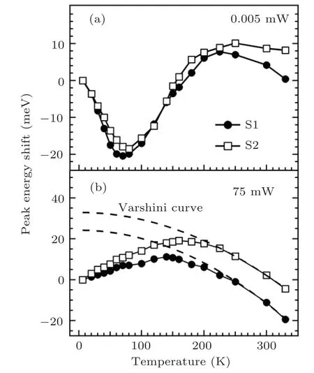
Fig.4. Temperature-dependent peak energy shift for S1 and S2 measured at(a)0.005 mW and(b)75 mW.
Furthermore, as the excitation power increases from 0.005 mW to 75 mW,it is found that both the“S-shaped”behavior for S1 and the “V-shaped” behavior for S2 as shown in Fig.4(a) evolve into an inverted “V-shaped” (increasingdecreasing)relationship(Fig.4(b))due to the carrier localization effect decreasing markedly.[31,36]Nevertheless,as a comparison, one can see from Fig.4(b) that the critical temperature corresponding to the maximum of the peak energy shift,is greater(160 K)for S2 than for S1(140 K);also, the depth of the localized states, which is estimated from the discrepancy between the curve of the peak energy shift versus temperature and the Varshni’s curve at low temperatures,[6,26]is greater(∼32.8 meV)for S2 than for S1(∼24.2 meV).These results indicate that S2 has a stronger carrier localization effect than S1, which is in good agreement with the aforementioned result. Moreover, it is also found from Figs. 1–4 that S2 has a stronger localization effect and QCSE than S1, but its linewidth is only slightly larger. The reason is not clear. It may be because S2 has a better homogeneity in the depth of the localized state than S1,[36]and this partially compensates for its stronger QCSE-induced linewidth broadening.

Fig.5. Excitation-power-dependent IQE for samples S1 and S2.
To explore the influence mechanism of the well layer growth temperature on recombination efficiency, the IQE,which is defined as the ratio of the PL efficiency at 300 K to the maximum PL efficiency at 6 K,is plotted as a function of excitation power for both S1 and S2(Fig.5). Here,the PL efficiency is defined as the integrated PL intensity divided by the corresponding excitation power density,and the maximum PL efficiency value at 6 K is assumed to be nearly 100% in the present study.[37,38]With the excitation power increasing from 0.005 mW to 75 mW, the IQE value of S1 markedly increases below 10 mW followed by relatively slowly increasing up to 75 mW, implying that the growing of photogenerated carriers can gradually saturate those non-radiative recombination centers thermally activated at 300 K, and this results in the carrier recombination mechanism in the MQWs gradually evolving from one of non-radiative recombination to radiative recombination;[31]in contrast, however, the IQE value of S2 first increases slightly below about 0.02 mW,then decreases slightly until about 0.2 mW, and finally increases markedly up to 75 mW. The excitation-power-dependent increase of the IQE value of S2 both in the initial excitation power range (<0.02 mW) and in the final excitation power range (>0.2 mW) is believed to be related to the dominant non-radiative recombination,similar to the description for S1 in Fig.5, but the excitation-power-dependent decrease of the IQE value of S2 in the intermediate excitation power range of 0.02 mW–0.2 mW, may correspond to the marked weakening of carrier localization effect. The explanations are also supported by the experimental fact that compared with S1,S2 exhibits a high IQE in the initial excitation power range below about 0.05 mW,which may be due to the stronger carrier localization effect as mentioned above,and a lower IQE in the high excitation power range above about 0.05 mW may mainly be because of the presence of more numerous defect-related nonradiative centers as confirmed in Fig.3. Moreover, the claim that there is a larger number of non-radiative centers in S2 than in S1, is also consistent with the experimental result that in contrast to S1,S2 does not exhibit excitation-power-dependent saturation trend of the IQE even in the higher excitation power range above 10 mW(Fig.5).
4. Conclusions
Excitation-power-dependent and temperature-dependent PL spectra of two different green InGaN/GaN MQW samples S1 and S2, in which InGaN well layers are separately deposited at a higher temperature of (745◦C) for S1 and a lower temperature (730◦C) for S2, are investigated. When the excitation power increases in an initial excitation power range below about 0.02 mW at 6 K, the peak energy remains almost unchanged while the linewidth narrows monotonically for both the samples S1 and S2, but the behavior of the excitation-power-dependent linewidth narrowing is more significant for S2 than for S1. The behaviors indicate that in the initial excitation power range, the emission processes of the MQWs for both the samples are dominated simultaneously by the carrier scattering effect and Coulomb screening effect, but both the scattering effect and the screening effect in the process are stronger for S2 than for S1; however,when the excitation power rises in the highest excitation power range above about 10 mW, the peak energy increases monotonically for both the samples, but the peak linewidth markedly broadens for S1 and significantly narrows for S2,indicating that the excitation-power-dependent Coulomb screening effect is stronger for S2 than for S1 in the highest excitation power range. The above results indicate that S2 has a higher amount of In content in the MQWs than S1 due to the lower growth temperature, and this results in the more significant compositional fluctuation-induced potential fluctuation and the stronger well/barrier lattice mismatch-induced QCSE. This explanation is also supported by the measurements of the excitation-power-dependent PL peak energy and linewidth at 300 K, the temperature-dependent peak energy,and the excitation-power-dependent IQE.
猜你喜欢
杂志排行

Chinese Physics B的其它文章
- Speeding up generation of photon Fock state in a superconducting circuit via counterdiabatic driving∗
- Micro-scale photon source in a hybrid cQED system∗
- Quantum plasmon enhanced nonlinear wave mixing in graphene nanoflakes∗
- Restricted Boltzmann machine: Recent advances and mean-field theory*
- Nodal superconducting gap in LiFeP revealed by NMR:Contrast with LiFeAs*
- Origin of itinerant ferromagnetism in two-dimensional Fe3GeTe2∗