二维过渡金属硫属化合物的大面积制备与应用研究进展
2021-02-26杨鹏飞石雨萍张艳锋
杨鹏飞,石雨萍,张艳锋
(1.北京大学前沿交叉学科研究院,2.工学院材料科学与工程系,北京100871)
1 Introduction
Recently,the discovery of graphene has inspired extensive explorations of two-dimensional(2D)layered materials[1,2].In particular,2D transition metal dichalcogenides(TMDs)[3,4],a huge family with abundant compositions,diverse crystal phases and sizable bandgaps,have attracted tremendous interests.Their remarkable physical and chemical properties,such as the indirect-to-direct bandgap transition[5],strong light-matter interaction[6,7],spin and valley coupling[8,9],and high electrocatalytic activity[10,11],were also uncovered by successive efforts.Some intriguing applications have been pursued,including electronic/optoelectronic devices[12,13],catalysis[14,15]and energy storage and conversions[16,17].Particularly,the rapid development of large-scale integrated electronics industry has brought up new requirements to the sample size,crystalline quality and thickness uniformity of 2D TMDs,for approaching the satisfactory performance of a single device and the large-area homogeneity of the device arrays.In this regard,the controllable synthesis of large-scale,high-quality TMDs is highly desired.
2D TMDs materials were firstly obtained by a mechanical exfoliation route using a scotch tape as the supporting media[5].Afterwards,liquid-phase exfoliation route was also exploited to produce TMDs flakes or powders in a low-cost and high-yield way[18].However,the derived TMDs products by these exfoliation methods usually possess small flake sizes(nanometer scale),uncontrollable thicknesses,and unsatisfactory quality,due to the existence of residual reagents and the involved uncontrollable violent force[19].Recently,chemical vapor deposition(CVD)has been developed as a scalable and high efficient route to grow large-scale high-quality 2D materials[20—26].This is because that,the CVD setup can be easily scaled up to the industrial level,the involved chemical reactant can be strictly controlled through vapor phase chemistry,and the growth substrates can be designed to facilitate different growth modes(surface catalyzed or segregation growth modes).With this approach,inch-scale single-crystal graphene monolayers have been successfully synthe⁃sized on single-/poly-crystalline Cu foils by different growth strategies(e.g.,van der Waals epitaxy[27],local precursor feeding assisted route[28],and substrate pulling route[29])in the CVD processes.Wafer-scale singlecrystal h-BN monolayers have also been obtained on molten Au substrates[30]and single-crystal Cu facets[31,32][e.g.,Cu(110)and Cu(111)],by the stitching of mono-orientated single-crystal domains.
In recent years,several CVD strategies have been designed to synthesize large-domain and thicknesscontrollable TMDs materials on various substrates[33—38].However,the large-area uniform growth of mono-or few-layer TMDs materials is still under way.The key challenges are as follows.First,the primary metal precursors having high melting points(MoO3:530℃,WO3:850℃,etc.)usually present variable release rates and nonuniform nucleation at the early growth stage,and thus inhomogeneous growth along the gas-flow direction[39].Second,the impurities or defect sites on the commonly used substrates usually induce preferen⁃tial nucleation and growth at these highly active positions,resulting in the formation of unnecessary additional layers.Third,the limited diffusion of precursors on growth substrates usually results in random thickness distributions from monolayer to few layers.Accordingly,the growth of large-scale thickness-uniform TMDs films requires sufficient and uniform delivery of metal precursors to the substrates,their isotropy diffusions on the atomically flat substrate surfaces,as well as the control of defects and nucleation densities on the substrates.
Generally,the small domain size and the high density of domain boundary are considered to imply negative impact on the crystalline quality of TMDs.Domain boundaries commonly appear in large-area,poly⁃crystalline TMDs films,which usually serve as conducting channels and charge carrier scattering centers,thus hampering the electrical and optical properties of the related devices[40—42].To tackle this,large-size TMDs films with few or even without domain boundaries are expected,since they provide the ultimate crystal⁃line quality without worsening from the defects.As known that,micrometer-sized TMDs domains are easily available,while the wafer-scale synthesis of single-crystal monolayers still remains a huge challenge,since the domain boundary will be formed when the adjacent domains are not oriented.In view of this,the epitaxial growth route through the seamless stitching of mono-oriented domains should be a more reliable strategy.
Alternatively,the high density of domain boundaries with abundant crystal defects can enrich the chemi⁃cal properties of TMDs towards new functionalities.For instance,the domain boundaries or the domain edges in monolayer TMDs have been demonstrated as catalytically active sites for hydrogen evolution reaction(HER).TMDs monolayers thus have the potential to serve as naturally abundant,cost-effective catalysts in electrocatalytic fields with regard to the traditional Pt-based caltalysts[43,44].At this point,introducing high density of domain boundaries or domain edges in the TMDs monolayers should be an effective way to enhance their HER performance.Given these requirements,considerable efforts have been devoted to the preparation of large-scale monolayer TMDs flakes/films with highly uniform thickness and nano-sized domains.
Herein,we provide a review of the latest CVD routes developed for the large-scale uniform growth of TMDs films,as well as their electrochemical applications.We summarize two classes of CVD growth ap⁃proaches from the viewpoints of precursor feeding route and substrate engineering,to realize the large-scale growth of 2D TMDs with uniform thickness.The internal growth mechanisms and parameter optimization pro⁃cesses are also intensively discussed.The popular applications towards large-scale integrated electronics and electrochemical catalysis are also summarized.Finally,an outlook of the challenges and future directions for the syntheses of wafer-scale TMDs films is provided.
2 Controlled Growth of Large-area Uniform 2D TMDs Films
In a typical CVD growth process of TMDs,transition metal oxides(e.g.,MoO3,WO3)and chalcogens powders are commonly used as metal and chalcogens precursors[45,46],respectively.Various experimental pa⁃rameters,such as the type of precursors,roughness of substrate,and gas flow rate,can influence the domain size,crystal quality,thickness and uniformity of the TMDs layers.To achieve the large-area uniform growth of TMDs,the most important premise is to ensure the homogenous nucleation at the initial growth stage.Herein,two strategies are summarized along this direction,especially for the large-area uniform growth of monolayer MoS2,through designing more practical metal precursor feeding strategy and selecting more suitable growth substrate,as will be discussed separately in this section.
2.1 Precursor Delivery Design
2.1.1 Face⁃to⁃face Precursor Delivery Route
It is generally believed that,the transport coefficient of the gaseous precursor under the low-pressure condition is several orders of magnitude higher than that under atmospheric-pressure condition[47].It means the precursor species in the low pressure condition have a relatively long diffusion distance and high masstransport rate.Therefore,the low-pressure CVD(LPCVD)route is,in general,more suitable for the uniform growth of TMDs over a decimeter scale along the gas flow direction.In the traditional LPCVD process,the metal precursors(e.g.,MoO3,WO3)and chalcogens(e.g.,S,Se)were placed at the upstream of the sub⁃strate.After being heated individually,their vapor phases were conveyed downstream by the carrier gases,and reacted with each other to deposit TMDs on the substrate[38].According to the deposition geometry between metal precursor and substrate,this method is referred as the“point-to-face”metal precursor supply route.However,due to the much higher melting points of the metal precursors(e.g.,MoO3:530℃,WO3:850℃)than those of the chalcogens(e.g.,S:103℃,Se:220℃),the volatilization and diffusion of the metal precursors were significantly limited.As reported by Aljarbet al.[48],in the LPCVD process,the concentration of metal precursor usually decrease quickly along the gas flow direction,while that of the chalcogens remains constant.Accordingly,both the coverage and domain size of TMDs are decreased with increasing the distance away from the metal source.Therefore,such“point-to-face”supply route is difficult to produce uniform monolayer/multilayer films even over several centimeter scale.To bypass this issue,a“face-to-face”metal precursor supply route was developed.
Recently,Yanget al.has reported the successful synthesis of 6-inch uniform monolayer MoS2film by using Mo foil as metal precursor,which was placed above the soda-lime glass substrate[49].Notably,due to the relatively high melting point of the Mo foil(ca.2600℃),the O2carrier was introduced into the furnace to oxi⁃dize the Mo foil for directly releasing chemically active MoO3−x(x=1,2).As shown in Fig.1(A),the Mo foil is folded as a bridge and placed on top of the glass substrate in a face-to-face configuration.Thus,the MoO3—xspecies arising from the oxidized Mo foil can be uniformly released into the gap between Mo foil and glass,resulting in homogenous nucleation and growth of monolayer MoS2over the entire glass surface.For compari⁃son,the point-to-face metal precursor supply route was also employed by using MoO3powder as feedstock.As shown in Fig.1(B),the MoS2/glass sample derived from the point-to-face metal precursor feeding assisted route shows a gradually fading brown color along the gas flow direction(from left to right),with the MoS2thick⁃ness varying from multilayer to continuous monolayer,and to discontinuous domains.In stark contrast,the sample derived by the face-to-face metal precursor assisted growth route presents a uniform color contrast over the entire glass surface.The corresponding optical microscopy(OM)images[Fig.1(C)]of the marked points in Fig.1(B)reveal the remarkable thickness uniformity over a decimeter scale.The representative Raman spectra with an identical frequency difference of 20.5 cm—1confirm its monolayer feature[Fig.1(D)].

Fig.1 Controllable synthesis of large⁃area uniform TMDs films by the face⁃to⁃face metal precursor supply assisted route
Except for this,the uniformly distributed sodium in the soda-lime glass was also confirmed as an effective catalyst by lowering the highest energy barrier of monolayer MoS2growth(the growth step from Mo2S2to Mo2S4)fromca.0.53 toca.0.29 eV,according to the theoretical calculations.Accordingly,a 6-inch uniform mono⁃layer MoS2film with the domain size(edge length of the triangular domain before merged)larger than 400µm was successfully synthesized at 720℃within only 8 min.Moreover,nucleation and growth of the second MoS2layer were found to be very difficult,probably due to the limited catalysts on the surface and the involved sur⁃face catalytic growth mechanism.Recently,alkali metal halides have been proved to be perfect promoters in facilitating the nucleation and growth of 2D TMDs materials[50,51].In light of these,the thickness controllable growth of wedding-cake-like multilayer MoS2flakes was also realized on the 6-inch soda-lime glass at 720℃by Yanget al.[52],using the NaCl-coated Mo foil as metal precursor and the similar face-to-face metal precursor feeding assisted growth route.The thicknesses of MoS2flakes were precisely tuned from bilayer to more than twenty layers by increasing the concentrations of NaCl solutions[Fig.1(E)].Based on the characterizations of the intermediate products,it was deduced that,the coated NaCl effectively facilitated the evaporation of Mo precursors by forming volatile MoOCl4,leading to the formation of bilayers and multilayers.Furthermore,the photodetector devices based on the monolayer-multilayer MoS2lateral junctions displayed a relatively high rec⁃tification ratio(ca.103)and extra high photoresponsitivity(ca.104A/W),demonstrating the relatively high crystal quality of the MoS2multilayers.
For the atmospheric-pressure CVD(APCVD)growth of 2D TMDs layers,the metal precursor is usually placed below or adjacent to the substrate,in view of the limited mass-transport rate under the atmosphere condition.The concentration or the deposition rate of the metal precursor is thereby hard to be controlled under such a short precursor-substrate distance.To solve this issue,Limet al.[53]developed a chemicalreactive-barrier-based approach to regulate the precursor flux.As schematically shown in Fig.1(F),a piece of NiO foam is used as a barrier and placed directly above the MoO3powder.The sapphire substrate is placed on top of the foam.During the CVD process,NiO reacted with MoO3and formed a stable NiMoO4compound,which effectively reduced the concentration of Mo precursors and the nucleation density on sapphire,allowing the maximum domain size up toca.170µm.Besides,the face-to-face deposition geometry between the MoO3source and substrate enabled a uniform distribution of reactants on the sapphire substrate.Thereby,a highly uniform monolayer MoS2film with an area of 2.5 cm×2.5 cm was successfully obtained[synthesized at 775℃for 10 min,Fig.1(G)].
In summary,the face-to-face metal precursor supply assisted CVD route was proved to be effective in achieving the homogeneous distribution of precursor,enabling the growth of uniform monolayer/multilayer films over a decimeter scale.The domain size of the continuous film can be effectively controlled by tuning the carrier-gas flow rate,the source-substrate distance and the precursor concentration,etc.This unique growth strategy is thereby proposed to be reliable for future scaling up of the production of TMDs layers.However,more effective control of the releasing rate of the metal-precursor should be further explored,considering of the extremely high melting points of various metal foil.
2.1.2 Coating of Precursor⁃solution Route
Comparing with the solid metal precursor powder,solution-processed precursor is more feasible to assem⁃ble on the growth template to form a homogenous film,enabling the uniform releasing of the metal source in the CVD growth process.From this perspective,a precursor feeding strategy was developed by spin-coating the metal precursor solution on a supporting template.Specifically,the metal precursor[e.g.,MoO3,(NH4)2MoO4]was first dissolved in a certain solute(e.g.,water,acetone)to make a precursor solution.Then,the solution was dropped/spin-coated on the substrate to form a thin film,which was then used as the metal source in the following CVD process.
Yunet al.[54]reported the successful synthesis of a 2 cm×3 cm uniform monolayer WS2film[Fig.2(A,B)]on the Au foil by using(NH4)6H2W12O40·x(H2O)(AMT)and H2S as precursors,viathe tungsten-sourcecoating route.AMT was dissolved in the deionized water and dropped onto an Al2O3plate.After drying in an oven,this precursor template was placed below the Au substrate in a parallel geometry,inducing the release of the metal precursor in a face-to-face manner.Notably,surface treatments(including annealing,chemical mechanical polishing,and acid treatment)to the Au foil substrates were conducted before the growth of WS2,in order to improve the substrate flatness.The continuous WS2film(synthesized atca.935℃for 15 min)presented an excellent thickness uniformity with the monolayer portion close to 100%.Meanwhile,the domain size of the continuous film was effectively tuned by varying the growth temperature.A relatively high growth temperature(ca.935℃)helped to increase the domain size toca.420µm(triangular edge length).The fabricated WS2-based field effect transistor(FET)showed a high electron mobility ofca.20 cm2∙V—1∙s—1and a high on-off ratio ofca.108at room temperature,confirming the high crystalline quali⁃ty of the WS2monolayers.
In order to further increase the domain size,Leeet al.[55]used a low-concentration solution-processed pre⁃cursor supply route and realized the CVD growth of large-scale MoS2monolayer.Specifically,small amount of MoO3(ca.0.01 mg)precursor was dissolved in NH4OH and then the mixed solution was spin-coated on a SiO2template,to supply Mo-source to the over positioned SiO2/Si substrate[Fig.2(C)].This method induced a relatively low supersaturation level of the metal precursor and hence reduced the nucleation density down to 32 nuclei mm−2over the entire substrate.Thereby,a 1 cm×2 cm uniform monolayer MoS2film[Region C in Fig.2(D)]was successfully synthesized within 5 min,with the domain edge length larger than 500µm.However,there are many unconnected triangular domains on the edges of the substrate(Region L and R),probably due to the insufficient precursor supply,through the metal precursor solution coating assisted growth route.

Fig.2 Controllable synthesis of large⁃area TMDs monolayers by the metal⁃precursor⁃solution⁃coating assisted CVD route
To further enhance the uniformity of metal precursor on the substrate,Zhuet al.[56]developed a MoS2—OH bilayer-mediated method[Fig.2(E)]and realized the growth of a 3 cm×3 cm uniform monolayer MoS2film[Fig.2(F)],with the domain edge length exceeding 200µm on arbitrary substrates(sapphire,mica,quartz,graphene,etc.).They added KOH(or NaOH)into the(NH4)2MoO4solution to introduce—OH groups in the precursor solution,and then spin-coated it onto the substrate.During the CVD growth process,the—OH groups were preferentially attached to the MoS2(001)surface,forming an S—Mo—S—OH bilayer structure.The occupation of—OH groups greatly impeded the vertical growth of MoS2,and constrained the growth only along the lateral direction.As shown in Fig.2(G),the uniform color contrast in Raman intensity mapping demonstrates the relatively high thickness uniformity of the resultant MoS2monolayer.Moreover,—OH groups can act as a protective layer to prevent MoS2from oxidation in air,and effectively reduced the sulfur vacancies and defects in the afterwards sample preservation and application processes.Accordingly,the fabricated FETs based on the MoS2monolayers presented a relatively high carrier mobility ofca.30 cm2∙V−1∙s−1,again confirming its high crystalline quality.
In order to ensure the uniform delivery of non-metal precursors,spin-coating and thermolysis of ammonium thiomolybdate[(NH4)2MoS4]were also used[57].Yiet al.[58]combined this with a roll-to-roll process and synthesized 50 cm long MoS2multilayer films on Ni foils.The thickness of MoS2was tuned by adjusting the concentration of(NH4)2MoS4precursor.However,it is rather difficult to obtain uniform monolayer film,due to the difficulty in controlling the amount and the distribution of metal precursor on the substrate surface.
In short,the precursor-solution-coating-assisted growth route was developed as a facile and economical route for the large-area growth of TMDs monolayers.This strategy usually combines with the face-to-face metal precursor supply geometry for the syntheses of various TMDs on arbitrary substrates.The domain size of the TMDs films can be well controlled by regulating the growth temperature,precursor spin-coating rate and pre⁃cursor solution concentration,etc.However,through the current precursor-solution-coating-assisted growth method,the thickness of the metal precursor film is still not strictly uniform,which usually results in the uncontrollable feeding of the precursors.
2.2 Substrate Engineering
Although much effort has been devoted to the large-scale and thickness-uniform production of 2D TMDs,the as-produced films are usually polycrystalline with the existence of many randomly orientated domains and domain boundaries.The boundaries are demonstrated to have a significant effect on the overall properties of the TMDs materials.For instance,domain boundaries can produce local strain that can either reduce or in⁃crease the bandgap depending on the tilt angle between the domains[59].Besides,they always act as charge car⁃rier scattering centers,and greatly hinder the charge transport and degrade the device performance[42].As dis⁃covered by Tsenet al.,the electron mobility across a domain boundary can be largely decreased by a factor of three[60].To fulfill the applications in electronics and optoelectronics,the growth of wafer-scale TMDs continu⁃ous films with few or even without domain boundaries is highly desired.In the past decade,the van der Waals epitaxial growth relying on the lattice matching between single-crystal substrates and the overlayers has been widely used to obtain large-size,single-crystal-like 2D films[31,61].That is because,the orientation of the mate⁃rial can be regulated by the surface symmetry of the substrate through their van der Waals interactions.For the epitaxial growth of TMDs,various lattice matched single-crystal templates,including the insulting substrates[62,63](e.g.,mica,sapphire),metallic substrates[64][e.g.,Au(111)]and 2D materials(e.g.,graphene,h-BN,GaN)[65—67],have been extensively explored.
Jiet al.[68]reported the growth of centimeter-scale uniform monolayer MoS2film[Fig.3(C)]on the latticematching mica substrate by using MoO3and S powders as feedstocksviathe LPCVD method.As illustrated in Fig.3(A),the lattice parameter of mica(amica=0.531 nm)approximates to 3aMoS2(ca.0.546 nm)with a small mismatch of−2.7%(negative sign means MoS2lattice is compressed),an epitaxial growth mode of MoS2was therefore induced on the mica substrate.The threefold symmetric MoS2domains were found to primarily align along two orientations on the six-fold symmetric mica,presenting a relative rotation angle of 60°.Fullcoverage MoS2monolayers were achieved at 530℃with the growth duration of 50 min.As shown in Fig.3(B),the atomic force microscopy(AFM)image of the nearly complete MoS2monolayer(with coverage ofca.90%)exhibits a nearly homogeneous color contrast,indicating its high thickness uniformity.Moreover,the striking⁃ly strong single PL peak(an excitonic emission)of as-grown sample provided a straightforward proof of the rela⁃tively high quality of the CVD-derived MoS2monolayer.From this prospective,the van der Waals epitaxial CVD method opens up a new avenue to achieve large-scale high-quality TMDs monolayers.
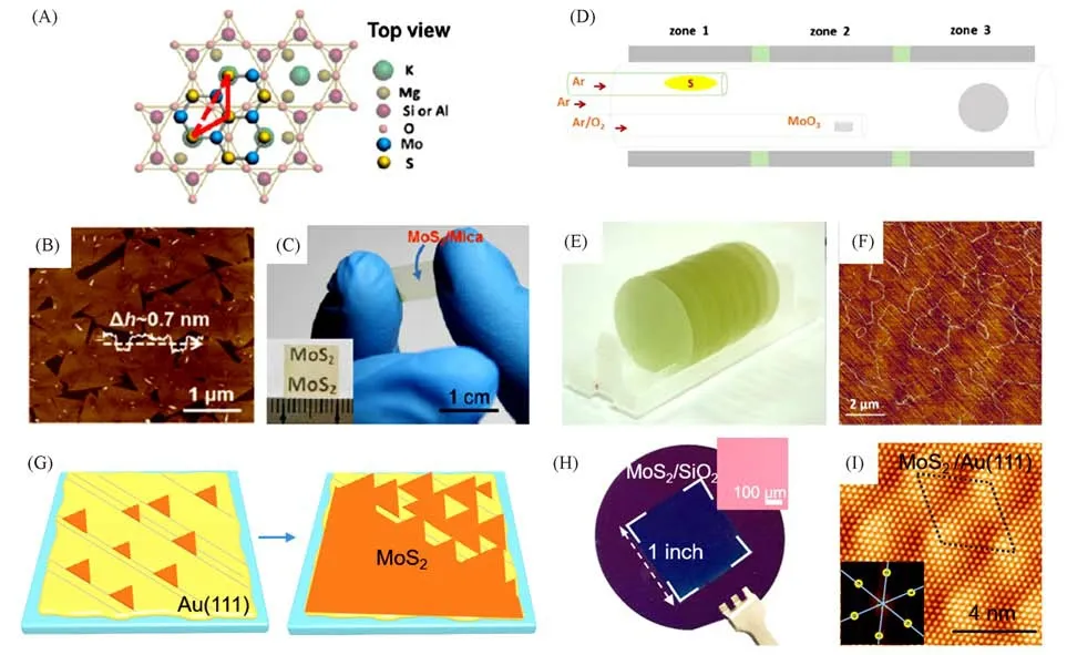
Fig.3 Epitaxial growth of monolayer TMDs on lattice⁃matching substrates
In addition to mica,the highly polished sapphire substrates are also commonly used to achieve the epitaxial growth of TMDs domains.Dumcencoet al.[62]reported the epitaxial growth of centimeter-scale mono⁃layer MoS2on the sapphire substrate through a APCVD route.The commensurability of the lattice of sapphire(aAl2O3=0.48 nm)with that of MoS2(aMoS2=0.24 nm)allows the epitaxial growth of MoS2on it with two energeti⁃cally preferential orientations(0° and 60° orientations).Besides,it was found that,the preparation of atomi⁃cally smooth terraces on the surface of sapphire by a standard annealing process(in air for 1 h at 1000℃)is the key to achieving such domain orientation.
Except for the substrate treatment process,Aljarbet al.[48]discovered that,the ratio between S and MoO3also plays a crucial role in the seed size and orientation of MoS2on sapphire.High S/MoO3ratio was necessary to form the nucleated seeds with small sizes,which can be easily aligned to the substrate lattice structure.In order to give a better control of the concentration of precursor,Yuet al.[69]placed the MoO3(530℃)and S(115℃)sources in separate temperature zones and employed independent carrier gas pathways(Ar/O2and Ar gases,respectively)for them[Fig.3(D)].Thereby,the batch production of 2-inch highly oriented continuous and uniform monolayer MoS2films(synthesized atca.930℃for 40 min)was achieved on the sapphire sub⁃strate following an epitaxial growth mechanism[Fig.3(E)].The derived epitaxial film was mainly stitched by 0° and 60° orientated triangular domains with the edge length ofca.2µm.The adjacent domains with same orientation stitched seamlessly and merged into a big single crystals,while the 0° and 60° stitched domains evolving a 60° domain boundary,which was directly recognized in the AFM image[Fig.3(F)]after exposing the sample in the moist atmosphere condition(with a humidity ofca.55%).Furthermore,the FET device arrays fabricated on the MoS2monolayers presented relatively high electron mobility and high on-off ratio,which have a narrow distributions and average atca.40 cm2∙V−1∙s−1andca.106,respectively.These values suggest the high thickness uniformity and high crystal quality feature of the epitaxial films.
By utilizing the above epitaxial substrates(mica and sapphire),the domains of the continuous films have been reduced to only two preferential relative orientations(0° and 60°).However,it is a huge challenge to eliminate the antiparallel domains and twin boundaries,because the six-fold symmetry of these substrates is in⁃compatible with the threefold symmetry of TMDs.Recently,Leeet al.demonstrated the successful synthesis of single-oriented WS2domains[70]and wafer-scale single-crystal WS2monolayer films,by substituting single-crystalline h-BN monolayers on a melting gold surface,with upstream conveyed(NH4)2S and spincoated Na2WO4as sulfur and metal sources,respectively.The internal mechanisms of the single orientated growth of WS2domains are still need to be further explored.
Very recently,Yanget al.[71]have realized the epitaxial growth of 3 cm×3 cm single-crystal MoS2mono⁃layer films[Fig.3(G)]on vicinal Au(111)surface by precisely controlling the domain orientation,and the stitching of the mono-oriented domains.The Au(111)facet was obtained by melting and resolidifying of the commercial Au foil on a tungsten template.During the APCVD process,the Au(111)substrate was placed on top of the MoO3powder in a face-to-face manner.As shown in Fig.3(H),the photograph and corresponding OM image of the transferred centimeter-scale monolayer MoS2film(synthesized atca.720℃for 8 min)present a homogenous color contrast on SiO2/Si,suggesting its high thickness uniformity.The unidirectional alignment and seamless stitching of the monolayer MoS2domains were comprehensively demonstrated using atomic-to centimeter-scale characterization techniques,such as low energy electron diffraction(LEED),trans⁃mission electron microscopy(TEM)and scanning tunneling microscope(STM).From the STM images of the as-grown monolayer MoS2/Au(111)shown in Fig.3(I),the MoS2atomic row can be observed to be wellaligned with the direction of the moirépattern or the lattice of Au(111),confirming the epitaxial relationship between monolayer MoS2and the Au(111)substrate.More importantly,the experimental results and firstprinciples calculations revealed that,the nucleation of MoS2monolayer was dominantly guided by the steps on Au(111),leading to highly oriented growth of MoS2along the<110>step edges.Such an orientation control strategy is expected to be broadly utilized on the single-crystal growth of other TMDs materials.
In summary,the van der Waals epitaxy route relying on the lattice-matching single-crystal substrate has presented great promise in the mono-orientation growth of the TMDs domains and in their merging into singlecrystal films.The epitaxial substrates(e.g.,mica and sapphire)were reported to be able to induce two prefer⁃ential relative orientations(0°and 60°)of TMDs domains,while the metallic substrates[e.g.,Au(111)]and 2D materials(e.g.,graphene,h-BN)templates enable the mono-orientation of the TMDs domains,thus have the potential to realize the wafer-scale growth of single-crystal films.
3 Applications of Large⁃area Uniform 2D TMDs Films and Their Hetero⁃structures
The rapid development of the CVD technique has shown its great potential to synthesize large-area,thick⁃ness-uniform and high-quality 2D TMDs materials.The explorations of their applications in various fields(electronics[72,73],optoelectronics[74],catalysis[75],etc.)have long been pursued.The vertically stacked hetero⁃structures by the stacking of TMDs and other 2D materials(e.g.,TMDs/TMDs,TMDs/h-BN,and TMDs/graphene heterostructures)have also been constructed to integrate their respective properties,affording extraordinary performances superior to their separate components[76—78].In this section,the recent progresses on the applications of large-area TMDs films and their heterostructures in electronic/optoelectronics and cata⁃lysts in HER are introduced.
3.1 Applications in Electronics and Optoelectronics
The well-known Moore’s law predicts that,the numbers of transistors per unit area will be doubled every two years,indicating that the size of each transistor will be shrunk continuously[79].However,traditional silicon transistors are reaching their physical limit nowadays.TMDs with the thickness of only several atomic layers have been recognized as one of the best candidate materials to extend the Moore’s law.Their surfaces are atomically flat and free from any dangling bonds,thus the electrons are less prone to scattering,and the charges can flow through them freely.In 2011,the first monolayer MoS2-based FET was reported with a high room temperature mobility ofca.200 cm2·V−1·s−1and a high on-off current ratio ofca.108,and the used MoS2sample was mechanically exfoliated by scotch tape[80].With the development of the CVD technique,the largearea,large-domain-size and high-quality TMDs monolayers have been directly synthesized and extensively employed to fabricate large-area integrated electronical/optoelectonical device arrays very recently.
In 2015,Kanget al.[81]prepared 4-inch scale high-quality monolayer MoS2and WS2films with excellent homogeneity on SiO2/Si substrates by using a metal-organic chemical vapor deposition(MOCVD)technique.The derived monolayer MoS2-based back gated FETs showed high electrical performance with average electron mobility ofca.30 cm2·V−1·s−1and on-off ratio ofca.106at room temperature.They also demonstrated the wafer-scale batch fabrication of 8100 monolayer MoS2FETs with a standard photolithography process,as well as the multi-level fabrication of vertically stacked FETs for three-dimensional circuitry.
In addition to these conventional rigid devices,transparent and flexible electronic/optoelectronic devices have also been exploited by virtue of the high transparency and good flexibility of 2D TMDs.Gaoet al.[35]pre⁃sented large-area flexible monolayer WS2FET device arrays on a polyethylene naphthalate(PEN)substrate,by transferring a 2-inch CVD grown monolayer WS2film onto the PEN substrate with pre-patterned electrodes(made by a standard photolithography).The mobility and on-off ratio were evaluated asca.0.99 cm2·V−1·s−1andca.105,respectively.Moreover,no electrical performance degradation was observed even after repeated bending to a radius of 15 mm for 100 times,indicating the great potential for the batch fabrication of large-area flexible devices.
Although great progress has been made on the FETs fabrication,the current experimentally reported mobility of monolayer MoS2is still one or two orders of magnitude lower than the theoretically predicted ones(200—410 cm2∙V−1∙s−1)[82].The possible reason for this discrepancy should arise from the existence of extrin⁃sic charge scattering from the interfacial Coulomb impurities,traps,and crystal defects in 2D TMDs samples[83].Among these,the Coulomb impurities at the semiconductor-dielectric interface is believed to be the most important limiting factor in current TMDs devices.To bypass this issue,the most effective approach is utilizing the insulating h-BN layer as a substitute for conventional dielectrics(e.g.,SiO2).To figure out the internal mechanism,Zhanget al.[84]synthesized h-BN monolayer and subsequently MoS2monolayer onh-BN/Au foilsviaa two-step LPCVD method[Fig.4(A,B)].The MoS2/h-BN stack based back-gate FETs showed a high mobility ofca.11.4 cm2∙V−1∙s−1[Fig.4(C)],which was about six times higher than that of the MoS2based ones.To investigate the reasons for the performance improvement,onsite scanning tunneling microscope/spec⁃troscopy(STM/STS)technique was utilized to exploit the band gap structures of monolayer MoS2on h-BN/Au and on bare Au substrates.A band gap increasing byca.0.25 eV was achieved for MoS2on h-BN/Au,with regard to that of pure monolayer MoS2/Au(ca.1.5 eV).This demonstrated that,the h-BN monolayer can par⁃tially block the metal-induced gap states for monolayer MoS2on Au,thus decrease the Schottky barrier height and increase the mobility of MoS2monolayer.
Theoretical and experimental analyses have indicated that,Fermi-level pinning,lattice strain,and metal induced gap states at the interface of metal-semiconductor greatly suppressed the charge carrier transport,re⁃sulting in performance degradations of the related devices[85].In view of this,the carrier mobility can be fur⁃ther improved by optimizing the interfacial contacts between electrodes and TMDs materials.Recently,metal⁃lic TMDs(m-TMDs)and semiconducting TMDs(s-TMDs)heterostructures have been reported to possess unique depletion profiles,leading to ultralow-resistance contacts.To confirm this,Jiet al.[86]synthesized MoS2/VS2lateral heterostructures on SiO2/Si substrates through a two-step CVD process.The polycrystalline monolayer MoS2nucleated from the vertices of multilayered VS2crystals,creating one-dimensional junctions with ultralow contact resistance(0.5 kΩ·µm).As a result,the field-effect mobility for the VS2-contacted MoS2device reached up toca.35 cm2·V−1·s−1,at least six times higher than that of the conventional Ni con⁃tacted ones(ca.5.5 cm2·V−1·s−1).However,the synthesized MoS2and VS2layers in this work were polycrys⁃talline and randomly oriented,which may influence the interfacial contacts.

Fig.4 Large⁃area electronic and optoelectronic devices based on TMDs and their heterostructures
To improve the interfacial quality,Zhanget al.[87]designed a robust van der Waals epitaxial route,and constructed a series of lattice-matched VSe2/MX2(M:Mo,W;X:S,Se)heterostructures[Fig.4(D)]through a two-step CVD method.The metallic VSe2was selected as the electrodes in view of its extra-high electrical conductivity ofca.106S/m[Fig.4(F)],which was 1—4 orders of magnitude higher than that of other conduc⁃tive 2D materials,and even comparable with that of silver and steel[88].The metallic VSe2multilayers prefer to nucleate at the energy-favorable edge site of the single-crystal s-TMDs monolayers,and then extend inward to form“void island”shaped structures[Fig.4(E)].By using the Kelvin probe force microscope(KPFM)charac⁃terizations,the formation of Schottky-diode or Ohmic contact-type band alignments was also determined for the VSe2/p-type-WSe2and VSe2/n-type-MoSe2stacks,respectively,which should facilitate their applications in high-performance optoelectronics and electronic devices with low-contact resistances.This work,thereby,provides an important reference for the device fabrication of such m-TMDs/s-TMDs heterostructures.
To fulfill the scalable integrations,Liet al.[89]developed a general synthetic strategy for the scalable fabri⁃cation of m-TMDs/s-TMDs heterostructure arrays.Specifically,periodic arrays of nucleation sites were firstly patterned on monolayer or bilayer s-TMDs(e.g.,WSe2,WS2,MoS2),on which the m-TMDs(e.g.,VSe2,VS2,NiTe2)selectively nucleated and grew to form m-TMDs/s-TMDs heterostructures.Diverse m-TMDs with designable arrangements and tunable lateral dimensions were thus successfully synthesized on s-TMDs substrates.A wide range of heterostructures(VSe2/WSe2,NiTe2/WSe2,CoTe2/WSe2,NbTe2/WSe2,etc.)were produced with atomically sharp and nearly ideal van der Waals interfaces,as evidenced by scanning transmis⁃sion electron microscopy(STEM)characterizations.In a further step,WSe2-based 2D transistor arrays were fabricated by using the stacked VSe2nanoplates as source and drain electrodes.The output characteristics showed a linear drain-source current-voltage relationship,indicating the formation of good Ohmic contact.Moreover,the devices with the CVD synthesized VSe2contacts present considerably improved carrier mobility(ca.100 cm2·V−1·s−1)and much narrower mobility distribution,comparing with the directly deposited Cr/Au metal contacts(mobility onlyca.10 cm2·V−1·s−1).
Except for the applications in high-mobility electronic devices,monolayer TMDs also attract great atten⁃tion in the optoelectronic devices due to their direct bandgaps and high absorption coefficients[90].Recently,several groups have reported the ultrafast interlayer charge transfer between MoX2/WX2(e.g.,WS2/MoS2,MoSe2/WSe2,MoTe2/WS2)bilayer heterostructures,due to the formation of type-II band alignments,where the conduction band minimum(CBM)and the valence band maximum(VBM)resided in the MoX2and WX2layers,respectively[91—93].Such type-II band alignments are conducive for the separation of electron and holes,and lead to greatly enhanced photocurrent generation.Tanet al.[94]fabricated arrays of graphene-contacted ver⁃tical WS2/MoS2heterobilayers by transferring pre-patterned graphene electrodes and metal bond pads onto the substrates with pre-transferred TMDs domains.All the 2D materials were grown by the CVD method,allowing the production of device arrays on a large scale.Due to the strong Coulomb interactions between WS2and MoS2monolayers,the photoresponsivity of the devices was increased by more than one order of magnitude,compar⁃ing with respective TMDs monolayers and bilayers,reaching 103A/W under an illumination power density of 1.7×10²mW/cm2.Moreover,the efficient charge transfer at the WS2/MoS2heterointerface and the long trap⁃ping time of photogenerated charges contribute to large photoconductive gain of 3×10⁴.This demonstrates the great application potential of hybrid TMDs heterostructures in high-performance photodetectors.
In short,the CVD-grown large-area uniform,high-quality TMDs provide robust platforms for the construc⁃tion of high-performance electronic and optoelectronic devices over large scale.Several routes have been put forward to optimize their performances,such as using h-BN as dielectric layer to reduce the charge disorder of the original substrates,utilizing m-TMDs or graphene as intermediate contacts to reduce the contact resistance between electrodes and semiconductors,fabricating type-II heterostructures to promote electron-hole separa⁃tion and the electron transfer.
3.2 Catalysts for Hydrogen Evolution Reactions
TMDs materials have also shown great prospective in catalyzing the electrochemical hydrogen(H2)pro⁃duction from water[95—99].Particularly,monolayer MoS2has been demonstrated as an effective catalyst for HER due to the following two aspects:(i)density functional theory(DFT)calculations have predicted that,the Gibbs free energy(ΔGH)of hydrogen adsorbed on Mo-terminated edge isca.0.1 eV,very close to that of Pt,which can facilitate both H*adsorption and H2desorption[44];(ii)the exchange current density of MoS2is also comparable to that of the noble metals,leading to high electron transfer rate and kinetic activity in HER[100].Taking these advantages,TMDs materials with unique electronic configurations have attracted tremendous interests in the HER research.To date,many strategies have been developed to optimize their HER catalytic activities,where the guiding principle was to optimize the active edge sites and activate the inert basal planes.
The domain edges or the boundaries of monolayer TMDs usually function as the active catalytic sites for HER[101].Exposing abundant domain edges/boundaries using nanostructured TMDs is a straightforward approach to improve the catalytic activity.To achieve this,Shiet al.[102,103]synthesized nano-sized,monolayer MoS2triangular domains with the edge length ofca.200 nm on the commonly used HER electrodes of Au foils,at a relatively low temperature(ca.530℃)through a facile CVD method[Fig.5(A)].As shown in Fig.5(B),the as-grown monolayer MoS2/Au catalysts present enhanced HER activities with increasing the coverage of monolayer MoS2.Especially,the 80% coverage sample exhibited a lowest Tafel slope ofca.61 mV/dec and a highest exchange current density ofca.38.1µA/cm2.Moreover,the strong electron coupling between monolayer MoS2and Au foil also contributed to the extraordinary HER activity.To further increasing the edge density over a large scale,Heet al.[104]fabricated 2-inch atomically thin MoS2films with sub-10 nm domains by means of Au-quantum-dots-assisted CVD route.The Au-quantum-dots were used to facilitate the MoS2nucleation and confine the domain size below 10 nm,so that the density of domain boundary was in⁃creased toca.1012cm−2.The electrocatalytic activity of the nanograin films was examined by a four-electrode micro-electrochemical cell,showing excellent HER performance with an onset potential of−25 mV and a Tafel slope ofca.54 mV/dec.
Beyond this,introducing catalytically active sites to activate the inert basal plane is also a possible route.As calculated by Liet al.,theΔGHfor the basal plane of intrinsic 2H-MoS2was as large asca.2 eV[105].How⁃ever,when increasing the concentrations of sulfur vacancy on the basal plane to 9%—19%,theΔGHvalue continuously decreased to about±0.08 eV,which was similar to or better than that of the edge site(ca.0.1 eV).In the experimental efforts,they introduced rich sulfur vacancies to the CVD-grown 2H-MoS2monolayers with a concentration of(12.5±2.5)%by the Ar plasma treatment.These sulfur vacancies served as new cata⁃lytic sites,and induced enhanced HER activity with an overpotential ofca.250 mV(at a current density of 10 mA/cm2)and a Tafel slope ofca.82 mV/dec.Besides,the local electronic structures of various types of sulfur vacancies were directly probed using STM/STS technique.It was confirmed that,the presence of sulfur vacan⁃cies introduced additional electronic states in the band gap,and enabled the band to move closer to the Fermi level,thus inducing the strengthening of H binding at these sites.
To optimize the activities of the inert basal planes,increasing their conductivities is also an important aspect,as it can facilitate the electron transfer between the interface of TMDs and electrolyte.To realize this,one commonly used method is to convert the phase of TMDs from semiconducting to metallic phases.The me⁃tallic 1T′-MoS2exhibits higher catalysis performance than 2H-MoS2,owing to its efficient electrical coupling with the substrate,rapid electron transport and plentiful catalytically active sites[106].Nevertheless,the direct synthesis of 1T′-MoS2is very challenging due to its metastable feature,making it easily convert to the stable 2H phase.Moreover,the formation energy of the 1T′phase(ca.0.84 eV per formula unit)is much higher than that of the 2H phase(ca.0.55 eV per formula unit).Nowadays,the preparation of 1T′phase MoS2main⁃ly relies on the transformation from 2H phase,which is induced by the post-growth treatments,such as lithium ion intercalation,electron-beam irradiation,and plasma hot electron transfer.However,these approaches can only produce a mixture of 1T′and 2H phased MoS2flakes,which are also not compatible with batch produc⁃tion.

Fig.5 HER performances of TMDs monolayers and their heterostructures
Recently,Liuet al.[107]have designed a potassium(K)-assisted CVD method for the direct synthesis of metallic 1T′-MoS2domains by using K2MoS4as growth precursor.As guided by the theoretical calculations,the 1T′phased MoS2became more stable than that of the 2H phase when the K concentration exceeded 44%.The metallic few-layer 1T′-MoS2flakes grown on highly oriented pyrolytic graphite(reversible hydrogen elec⁃trode)presented relatively high catalysis performance with the overpotential at a current density of 10 mA/cm2and Tafel slope of about−205 mV and 51 mV/dec,respectively,much lower than those for 2H-MoS2flakes(about−286 mV and 70 mV/dec,respectively).These results suggested the great application potential of 1T′-MoS2as a high-performance catalyst.
Meanwhile,various m-TMDs(e.g.,TaS2)were employed as efficient catalysts in HER due to their high conductivities and abundant catalytically active sites.Shiet al.[98]fabricated thickness-tunable 2H-TaS2flakes and centimeter-scale ultrathin films on gold foilsviadesigned LPCVD and APCVD routes,respectively.The 2H-TaS2flakes(thickness ofca.150 nm)showed a Tafel slope ofca.33 mV/dec in HER,comparable to that of Pt(ca.31 mV/dec),possibly due to the existence of abundant active sites at edges and basal-planes.Recent⁃ly,Huanet al.[108]designed a universal synthetic route for the scalable synthesis of m-TMDs(e.g.,1T-TaS2,V5S8,and NbS2)nanosheets on water-soluble microcrystalline NaCl crystals templatesviaa facile APCVD route.The derived 1T-TaS2flakes with uniform thickness and domain size were proved to be high-efficiency electrocatalysts in HER.
An alternative approach to promote the electron transport between TMDs and electrolyte is to combine TMDs with other conductors,such as graphene,carbon nanotube,and metal foil[109].Shiet al.[110,111]reported the direct synthesis of monolayer MoS2/graphene heterostructure on the conductive Au foil substrate[Fig.5(C)]through a two-step CVD route.By using the STM/STS characterizations,a dramatic decrease of the bandgap of monolayer MoS2was observed,which reduced fromca.2.20 toca.0.30 eV at the domain edge(within a later⁃al distance ofca.6 nm).This confirmed that,the inserting of graphene between MoS2and Au substrate can ef⁃ficiently suppress the charge recombination and improve the interfacial charge transfer.In consequence,the MoS2/graphene/Au samples presented much lower onset potential(ca.90 mV)and relatively small Tafel slopes(52—60 mV/dec),as compared with monolayer MoS2on Au foils(Tafel slopeca.70 mV/dec)[Fig.5(D)].Besides,it was reported that,the hydrogen recombination barrier was reduced at the Mo-terminated edge of the MoS2/graphene hybrid,which should explain the enhanced HER efficiency from a theoretical point of view.
In addition to the above strategies,fabrication of TMDs/TMDs vertical heterostructures possessing type-II bandgap alignment feature has manifested advantages in terms of the efficient separation of electron-hole pairs,which can facilitate the photocatalytic application in HER.Shiet al.[112]directly synthesized MoS2/WS2and WS2/MoS2heterostructures on Au foils through a designed growth-temperature-mediated two-step CVD strategy.As shown in Fig.5(E),the as-grown MoS2/WS2/Au foil demonstrates higher photocatalytic activity than those of individual MoS2,WS2monolayers and WS2/MoS2stacks.This was explained from its stepwise type-II band alignment feature,which facilitated the effective electron-hole separation,as well as the fast elec⁃tron transfer kinetics[Fig.5(F)].
In summary,2D s-TMDs materials(especially monolayer MoS2)have emerged as potential substitutes for Pt in electrocatalytic and photocatalytic HER.To improve the HER performance of individual TMDs,several strategies have been developed to increase the active edge sites and activate the inert basal planes,such as maximally exposing the edges,introducing sulfur vacancies,and transforming the phase to metallic phase.Furthermore,TMDs-based heterostructures have also shown great potential in HER due to their fast charge transfer and unique band alignment features.The CVD method enables the precise control of the flake thickness,domain size and phase state,and thus the amount of the catalytically active sites of the derived materials,which provides us fertile platforms to explore the internal catalytic mechanisms.
4 Summary and Prospect
This topic review provides a comprehensive introduction of the recent progresses on the CVD syntheses of large-scale,thickness-uniform,high-quality TMDs materials,and discusses their versatile applications in electronics,optoelectronics and electrocatalysis related fields.The large-scale uniform growth of TMDs films rely on the homogenous nucleation at the initial growth stage.Thereby,two key strategies have been summa⁃rized and discussed in detail.The homogenous supply of precursors is vital for the nucleation process,as can be realized by tuning the partial pressure and the precursor delivery route in the CVD growth process,the layer thickness can also be modulated accordingly.The face-to-face precursor feeding route and the coating of precursor-solution assisted growth routes are proved to be effective in ensuring the homogenous supply of the metal precursors.Besides,the strategies of substrate engineering,such as the pretreatment of the substrate surface and the selection of lattice-matching single-crystal substrate,also play important roles during the CVD synthetic process.In particular,the van der Waals epitaxial strategy based on the single-crystal substrate can precisely control the orientation of the composite domains to a specific direction,inducing the growth of largearea single-crystal TMDs films.
Although many attempts have been made at the growth of TMDs films over a large scale,the in-depth investigations related to the scalable syntheses and practical applications of 2D TMDs are still at the initial stages.Firstly,the domain sizes of TMDs achieved by CVD methods are mostly less than 500µm(triangular edge length),and the synthesis technology is still less mature than that for the graphene growth.It is practica⁃ble to improve the domain size of TMDs by learning from the growth of graphene,such as by using local feeding of reactants,pulling the growth substrates,and introducing etchants at the growth process.Secondly,wa⁃fer-scale single-crystal growth should be a very urgent issue.Normally,the epitaxial grown TMDs films com⁃posed by 60° rotated domains possess inevitable twin boundaries.More unique single-crystal epitaxial sub⁃strates,especially the metal facets,should be further explored for the mono-oriented growth of individual do⁃mains,and for their merging into wafer-scale single-crystal film.Thirdly,the direct fabrication of large-scale van der Waals heterostructures still remains a great challenge.Moreover,in order to catch broader interests from the society,more accessible applications based on large-area TMDs or their heterostructures should be developed,such as the applications in wearable and flexible devices,sensors,displays.
This work is supported by the National Key Research and Development Program of China(No.2018YFA0703700),the National Natural Science Foundation of China(Nos.51991344,51991340,51925201,51861135201)and the Beijing Natural Science Foundation,China(No.2192021).
