单元素二维材料及其衍生物作为电荷传输层在太阳能电池中应用的研究进展
2021-02-26林生晃傅年庆鲍桥梁
林生晃,傅年庆,鲍桥梁
(1.松山湖材料实验室,东莞523808;2.华南理工大学材料科学与工程系,广州510641;3.蒙纳士大学材料科学与工程系,维多利亚3800,澳大利亚;4.中国科学院长春光学精密机械与物理研究所应用光学国家重点实验,长春130022)
1 Introduction
Since the rapid development of consumer electronics,electrical vehicles,and grid storage,scientists are exploring new kinds of energy alternatives to meet the world’s ever-growing energy demands due to the ex⁃tremely limited current energy sources of fossil fuels like oils and coals in the world.As expected,the solar energy is a very clean and sustainable energy source that can offer inexhaustible supply of energy for human so⁃ciety.Especially for many issues faced by humans,the clean solar energy can not only solve the problems of the environmental concerns,but also meet the growing demands of energy expenditure.In terms of the existing solar energy technologies,photovoltaics(PV)is a powerful and successful method to directly convert solar energy into electric power.Except for the current commercially available silicon-based solar cells,scientists are also seeking novel materials to be used in solar cells to improve their energy efficiency,stability and lower the cost.Among them,Novoselovet al.[1]made a notable discovery of fabricating a single-layer twodimensional(2D)graphene in 2004,which won the Nobel Prize of Physics in 2010 and revealed the thinnest material in the universe.After that,many other graphene-like 2D materials are gradually investigated,includ⁃ing MoS2[2],WS2[3],black phosphorus(BP)[4—7],PtSe2[8—10],etc.Such studied 2D materials possess many ex⁃traordinary novel properties,such as excellent conductivity,high photodetectivity,high on-off ratio and high carrier mobility compared with traditional semiconductors.Driven largely by the search for atomically thin ma⁃terials beyond graphene with unique and exciting properties,much attention has been paid for the research in elemental materials over the past few years[11].The successful preparation of non-graphene elemental 2D mate⁃rials such as silicene and BP was the beginning of an ever-expanding list of elements that have been predicted or synthesized in atomically thin form.Up to now,15 types of elemental 2D materials have been experimental⁃ly confirmed or theoretically predicted by many research groups[12].There are some review articles about prepa⁃ration and applications of elemental 2D materials[12—14],but few concentrates on their energy applications of so⁃lar cells.In this review,we will conclude very recent studies on elemental 2D materials and hope to provide a comprehensive overview and new insights into its solar energy applications.Generally,we will discuss the structure and properties of elemental 2D materials first,then introduce the methods for preparing diverse ele⁃mental 2D materials.Furthermore,we will summarize the recent progress of elemental 2D materials,including antimonene,bismuthene,BP,borophene and graphene as shown in Fig.1,as transport layers in solar cells.Finally,our insights into the challenges and opportunities of elemental 2D materials in this research field will be proposed.
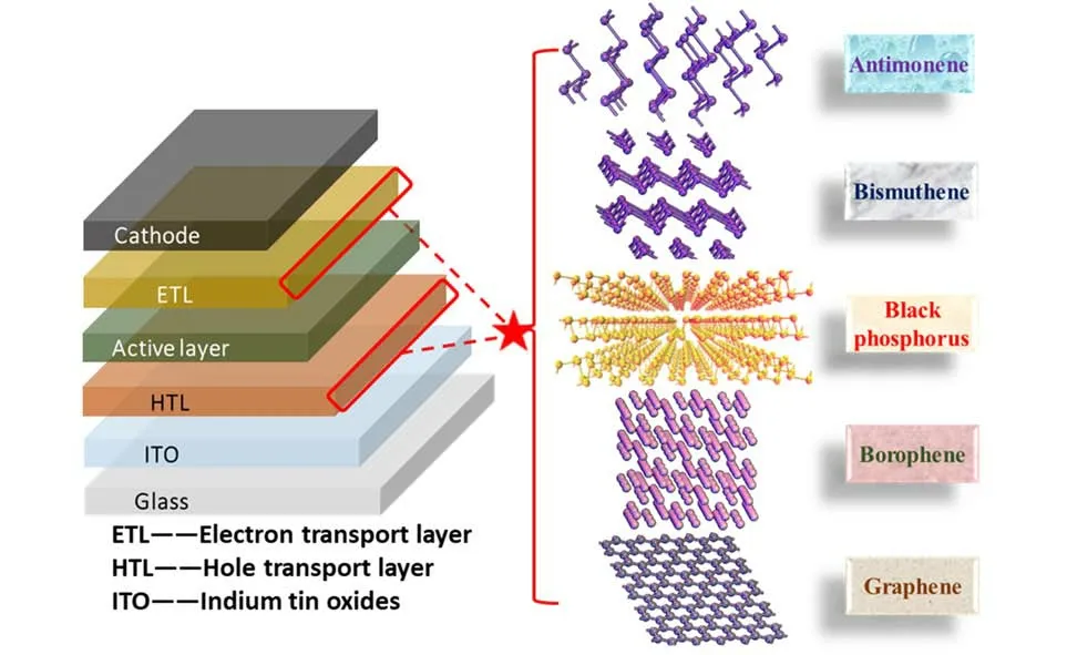
Fig.1 Schematic illustration of using elemental 2D materials as transport layers in solar cells
2 Crystal Structures of Studied Elemental 2D Materials
As we know,the intrinsic properties(including electronic,optical,thermal,mechanicetc.)of elemental 2D materials are strongly correlated to their crystal structures,i.e.,stacking sequence or the arrangement of atoms in the lattice.Comparing with their bulk form,elemental 2D materials also have allotropes with different crystal lattices,which have either been experimentally or theoretically investigated.
As reported,layered carbon has an ideal structure of honeycomb lattice,possessing four valence elec⁃trons per carbon atom to completely fill all of the bonding electronic orbitals.Besides carbon,other elements(Si,Ge,and Sn)in Group IV also share electronic characteristics similar to carbon but have preferably more hybridization states betweensp2andsp3,which lead to buckled crystal lattice structures rather than planar one as observed in graphene[15,16].Recently,Matusalemet al.[17]demonstrated that the stable silicene and ger⁃manene have large honeycomb dumb-bell(LHD)geometry but stanene has the MoS2-like symmetry.The struc⁃ture of stanene was theoretically investigated[18—20]by following the study of germanene and silicene[21,22].On the other hand,Si,Ge and Sn do not have a naturally occurring 3D-layered parent material,which means their corresponding freestanding 2D materials should be prepared by a more powerful bottom-up method.Up to now,stanine,silicene and germanene can only be grown on metallic substrates,for example Si and Ge on no⁃ble metal surfaces and Sn on Bi2Te3[23—27].
Among the reported elemental 2D materials,there are only five types of them being employed in the pho⁃tovoltaic applications.Fig.2(A)shows the overview of elemental 2D materials explored through experimental or theoretical approaches in literature[4,23,24,28—38],and the elemental 2D materials marked by pentagram stars are the ones we reviewed in this article.A roadmap for the trend of exploring elemental 2D materials can be found in Fig.2(B).Except for the widely studied graphene,phosphorene,borophene,antimonene and bismu⁃thene are the recent rediscovered 2D materials.As for groupⅢelements,a number of allotropes of 2D boron(borophene)have been theoretically predicted due to its complex multiatomic unit cells,which might be relative to lower number of valence electrons in groupⅢelements[39].Meanwhile,boron has also been re⁃vealed to possess a metallic layered structure with buckled triangular motifs[40,41].In terms of bulk BP,it has three crystalline structures:orthorhombic,simple cubic,and rhombohedral.Similar to graphite,adjacent BP atomic layers are stacked together through weak van der Waals interaction while the single layer is formed bysp3phosphorus atoms through covalently bonding.Owing to thesp3hybridization,each P atom is saturated and covalently bonded to three neighboring P atoms and has one lone-electron pair,leading to a quadrangular pyra⁃mid structure resembling a puckered honeycomb structure,which induces a highly asymmetric band structure and unique in-plane anisotropic properties[42].Such unique structural properties of BP make it possess different lattice constants for the armchair(4.37Å,1Å=0.1 nm)and zigzag edges(3.31Å)[43].Antimonene and bismuthene,as members of the group V elemental 2D materials,are also theoretically expected to have puckered structures.It has been revealed that antimonene crystals with buckled structure showed to be stable in air and chemically robust[44].Meanwhile,antimonene is also predicted to have different degrees of anisotropy in mechanical properties[45].Bismuthene,the largest of the group V elements,has been demonstrated to exist in the buckled[Bi(111)]and puckered[Bi(110)]phases through both theoretical predictions and experimen⁃tal observations[46,47].
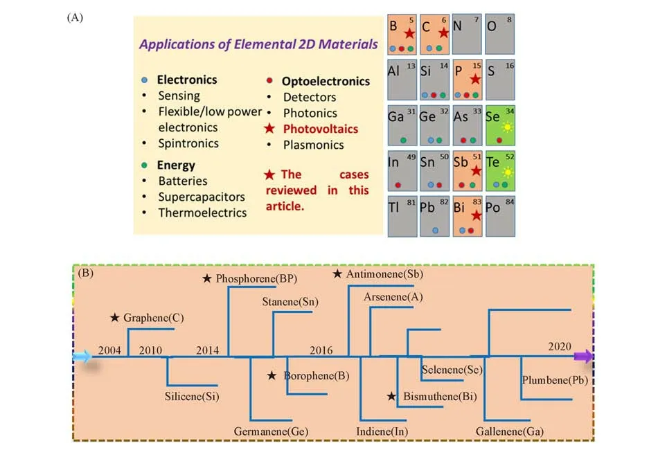
Fig.2 Overview of elemental 2D materials explored through experimental or theoretical approaches(A)and a roadmap of several recent elemental 2D materials being investigated in experiments or theory(B)
3 Synthesis and Processing
As reported,the electronic and optoelectronic properties of elemental 2D materials are much related to their structural characteristics which are usually induced by the synthesis and assembly process.There exist two common approaches for preparing elemental 2D materials,called top-down and bottom-up in short.These two approaches include mechanical or liquid-phase exfoliation and chemical vapor deposition(CVD)or epitaxial growth process[48],which provide a great platform to synthesize multi-types of elemental 2D materials for various potential applications.In this section,we will provide a short summary of different synthesis methods for fabricating elemental 2D materials,including antimonene,bismuthine,borophene,graphene and phos⁃phorene.
3.1 Top-down Approach
Mechanical or liquid-phase exfoliation,a so-called typical top-down method,is a usual way for preparing elemental 2D materials through breaking the weak van der Waals interaction between the layers in their bulk materials under the external driving forces.Since the first demonstration of monolayer graphene exfoliated by scotch tape[1],this simple and fast approachable exfoliation has been employed as a useful technique for fabri⁃cating high-quality,few-layered single-crystal elemental 2D materials[Fig.3(A)].The mechanically exfoliated 2D materials possess high-quality with few defects,which reveal remarkable fundamental electronic and optoelectronic properties.However,this technique is seriously restricted to practical applications due to the limited size of 2D materials.Liquid-phase exfoliation[Fig.3(B)]is another top-down method which refers to breaking a layered crystal into 2D materials by suspending the crystal in a solvent and blasting the crystal with ultrasonic energy.In this process,the interfacial tension between the materials being exfoliated and the liquid medium should be minimized to stabilize the as-prepared 2D flakes,realizing the existence of good interac⁃tions[49].Thus,moderate solvents(e.g.,ethanol andN-methyl-pyrrolidone)or intercalators(e.g.,butyllithium and metal naphthalenide)should be selected to effectively exfoliate the bulk materials[50—54].For exam⁃ple,large-scale 2D BP can be prepared through the liquid-phase exfoliation method in many solvents[49].Most of the reported liquid-phase exfoliation methods for preparing 2D materials are of low cost and provide high yield.It should be noted here that the crystal quality of liquid-phase exfoliated 2D materials is often reduced and there exist many functional groups or residual solvent and ions on the surface of 2D materials,which would affect their electronic and optoelectronic properties.It is noted here that liquid-phase exfoliation method is an ideal technique for providing scalable production of 2D materials when they serve as carrier transport layers in photovoltaic devices.
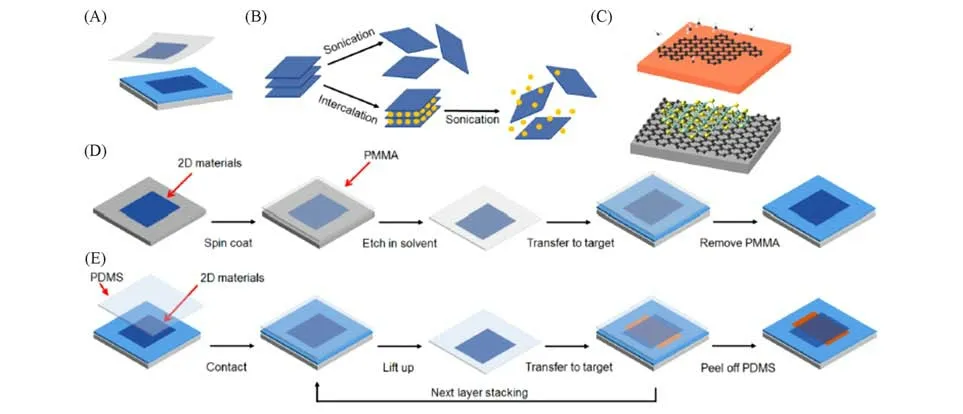
Fig.3 Mechanical exfoliation(A),liquid⁃phase exfoliation(B)and CVD(C)approaches for the synthesis of 2D materials[48]
3.2 Bottom-up Approach
Although liquid-phase exfoliation process can realize scalable production of 2D materials,its applications in many fields are still limited,such as large-area integrated circuit,which requires large scale and continuous films.Another method,called bottom-up approach,is more suitable for the synthesis of large-area 2D materials.Among of the bottom-up approaches,chemical vapor deposition(CVD)is a common technique to prepare large-scale and high-quality uniform 2D materials[Fig.3(C)].For example,the continuous and highquality graphene film can be successfully grown on different metal substrates(e.g.,Cu,Ni)[55—58]by using liquid,gas,or even solid carbon sources[59—61].Here the surface segregation/precipitation or surface adsorp⁃tion process of carbon on the surface of metal substrates is attributed to the growth mechanism of graphene[62].The growth process of graphene on metal substrates include three steps:(1)pyrolysis of hydrocarbon;(2)ad⁃sorption,dehydrogenation and diffusion of carbon species on or into metal;(3)nucleation and crystal growth.Based on this three growing-steps,large-scale graphene can be easily prepared.As predicted,other 2D mate⁃rials(not only elemental 2D materials)could also be grown on metal substrates using the similar growth pro⁃cess,including h-BN[63—66],MoS2[67—69],borophene[70]and so on.
3.3 Transfer and Assembly
The high-performance electronic and optoelectronic devices based on 2D materials require an efficient and non-destructive transferring process.Among the reported transfer techniques,a polymer-protected[e.g.,PMMA,poly(methylmethacrylate)]wet transfer method has been widely studied and usually employed for me⁃chanically exfoliated or CVD 2D materials[55,71].As reported,PMMA was first spin-coated onto the surface of 2D material,and then the substrates were removed using a certain solvent including etchants,e.g.,etching SiO2in a NaOH solution or Cu in a FeCl3solution.After that,PMMA with target 2D materials was transferred onto other substrates and PMMA could be removed using organic solvent[Fig.3(D)].It should be noted here that there still are some residual polymer on the surface of 2D materials even if the wet transfer method is con⁃sidered to be a powerful technique.This residual polymer could remarkably affect the electrical properties of 2D materials[72].Meanwhile,there also exist many wrinkles and cracks on the surface of 2D materials during wet transfer process,which has a negative effect on the performances of devices fabricated on 2D materials.In contrast,a so-called dry transfer technique seems to be an effective method for solving the above problems and has been developed by some investigators[73—75].As shown in Fig.3(E),the poly(dimethylsiloxane)(PDMS)stamp was used as a medium by first peeling off one 2D material from the substrate and then contacting to other 2D materials to form stacking layers after lift-off the stamp.More stacking layers with clean surface can be obtained through repeating the above procedure.Briefly,most of layered bulk materials(include elemental or compound 2D materials)can be exfoliated into monolayer or few-layer formsviawet or dry transfer rocess.
4 Applications of Elemental 2D Materials as Charge Transport Materials in Solar Cells
In the past decade,the emerging perovskite solar cells(PSCs)and organic photovoltaics(OPVs)have at⁃tracted tremendous interests due to their low-cost and rocketed development in efficiency[76—86].So far,the PSCs have reached a certified champion power conversion efficiency(PCE)of 25.2%,while a PCE record up to 17.4% was achieved for OPVs[86].In PSCs and OPVs,the charge transport layers[namely electron trans⁃port layer(ETL)and hole transport layer(HTL)]are commonly indispensable for achieving high-efficiency de⁃vices due to their ability to effectively separate the photo-generated electron-hole pairs and transport the charge carriers toward the corresponding collectors.An efficient charge transport material should possess:(1)proper energy level that can extract one kind of charge carrier(e.g.,ETL for electrons)from the excited absorber but blocks the other,(2)outstanding electrical properties with high conductivity to enable fast charge transport.For example,the most widely used TiO2as an ETL with spiro-OMeTAD as an HTL possess electron and hole motilities ofca.1 cm2·V−1·s−1andca.10−3cm2·V−1·s−1[87,88],respectively,which are much lower than those of perovskite absorbers and dominate the limitation for further improvement in PCE of PSCs.To this end,moni⁃toring the energy band and charge transfer/transport properties of ETL and HTL are of vital importance toward high-efficiency solar cells.
In recent years,many conventional 2D materials that have excellent optical and electrical properties,tunable energy band are regarded as promising alternative ETL and HTL materials for solar cells.These 2D materials include graphene,transition-metal dichalcogenides(TMDs,such as MoS2,WS2,SnS,InSe,etc),and so on[89—92].Besides the conventional ones,various emerging 2D materials,such as black phosphorus(BP),antimonene,bismuthene,borophene have also been intensively studied as functional layers in PSCs and OPVs.In the following sections,we will summarize the recent advancements in studies that explored the elemental 2D materials as ETL and HTL materials or interface modifiers for PSCs and OPVs.
4.1 Graphene and Its Derivatives as ETL or HTL for PSCs and OPVs
The single layer of graphite with a two-dimensional carbon network structure enables the graphene versa⁃tility and unique properties,such as excellent flexibility and mechanical strength,superior transparency in the visible spectrum(>97%),huge specific surface area(>2600 m2/g),and outstanding electrical conductivity(ca.104S/cm)[93—98].Since the breakthrough discovery by Novoselovet al.in 2004[1],graphene and its deriva⁃tives,including chemical functionalized graphene,graphene oxide(GO)and elemental doped graphene(Fig.4)[99,100],have become the most attractive elemental 2D materials that were widely exploited as charge transport materials in solar cells,with great progress for improving the efficiency of the devices[89—94].Moreover,the replacement of some conventional HTL and ETL materials by graphene or its derivatives can avoid their detrimental effects,such as the UV-induced catalytic degradation activity of TiO2-ETL toward perovskite,the hygroscopicity of doped Spiro-OMeTAD,and the acidity of PEDOT:PSS,and thus improve the long-term stability of the devices.
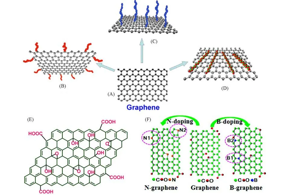
Fig.4 Schematic illustration of functionalized graphene by various strategies[99]
4.1.1 Pristine Graphene as Charge Transport Materials for PSCs and OPVs
As discussed above,pristine graphene can be obtained by the up-bottom methods,including mechanical/chemical/ultrasonic/electrochemical exfoliation of graphite,and by bottom-up approaches such as CVD pro⁃cess.Taking the CVD approach as an example,it is able to produce continuous large-area pristine graphene film with high-quality and controllable layers.This pristine graphene with zero-band gap energy level endows itself high charge carrier mobility for both electrons and holes,which makes it possible to be used as both elec⁃tron transport material and hole transport material for solar cells.Capassoet al.[101]transferred the CVD pro⁃duced graphene onto the indium tin oxide(ITO)/glass substrate and used as HTL for PBDTTT-C-T∶PC70BM blend based OPVs,attaining a PCE of 5%,similar to the reference cells made with state-of-the-art PEDOT∶PSS as HTL materials.Bonaccorsoet al.[102]obtained the graphene ink by ultrasonic exfoliation of the graphite flakes and employed it as electron acceptor for organic ternary solar cells,which led to an 18% enhancement in PCE of the device due to the improved exciton dissociation and electron transport associated with the better energy level alignment and the high electrical conductivity of the graphene.So far,there have been few studies on using pristine graphene directly as a charge transport material for solar cells.The hydrophobic nature of the graphene is one of the most challenging issues limiting the use of pristine graphene as HTL or ETL mate⁃rials for solar cells due to poor wettability of the precursor solution to the underneath graphene layer[103].More⁃over,the high manufacturing costs,tedious optimization,poor solubility of the pristine graphene also hamper its widely application in solar cells[94].In contrast,pristine graphene is more widely used to prepare conduc⁃tive electrode to replace ITO or FTO(fluorine-doped tin oxide)based substrate for solar cells,due to its excel⁃lent conductivity,high transparency,and good flexibility[104—106].
4.1.2 Graphene Oxide(GO)and Reduced Graphene Oxide(rGO)as Charge Transport Materials for PSCs and OPVs
Graphene oxide,commonly obtained by the modified Hummers method,is one of the most important de⁃rivatives of graphene.Due to the presence of functionalized oxygen groups in the forms of hydroxyl,epoxy,or other carboxylic acid groups on the plane and at the sheet edges[Fig.4(E)],GO is easily dispersed in water and various organic solvents,which gives GO the possibility of wide applications in a variety of fields.More importantly,GO contains a mixture ofsp2-andsp3-hybridizations,providing huge opportunities for tailoring its electronic(e.g.,conductivity)and optoelectronic(e.g.,work function and bandgap)properties by manipu⁃lating the size,shape and relative fraction of thesp2-hybridized domains of GO for different applications[107—110].
Chenet al.[111]demonstrated in their work that the deposition of GO film from a neutral solution between the photoactive poly(3-hexylthiophene)(P3HT)∶phenyl-C61-butyric acid methyl ester(PC61BM)layer and ITO electrode can effectively extract the photo-generated holes and reject the electron,leading to a decrease in electron-hole recombination and leakage currents.The obtained polymer solar cells gain a similar high PCE(3.5%)that comparable to the device with a PEDOT∶PSS based HTL[111].Smithet al.[112]also obtained a poly[N-9″-heptadecanyl-2,7-carbazole-alt-5,5-(4′,7′-di-2-thienyl-2′,1′,3′-benzothiadiazole)](PCDTBT):[6,6]-phenyl C71 butyric acid methyl ester(PC71BM)based OPV with 5% efficiency by using GO as HTL.Wanget al.[113]transferred thin GO film,which was obtained by continuous oxidization of CVD-graphene,on⁃to PCDTBT:PC70BM based solar cells as the ETL by a stamping process and a PCE of 6.72% was yielded.Besides being employed as HTL and ETL for OVPs,GO is also widely used as hole transport materials for PSCs[114—116].
As mentioned above,GO is composed ofsp2-andsp3-hybridized carbon atoms,and the C—O bonds are covalent,which thus disrupts thesp2conjugation of the hexagonal graphene lattice,making GO an insula⁃tor[111,117].Therefore the electronic and optoelectronic properties of GO can be readily tuned by adjusting the ra⁃tios ofsp2-andsp3-hybridizations,which will thus greatly influence conduction types(electron conductivity,hole conductivity,or insulation)and thereby the performance of the resultant solar cells.Zibouche’s firstprinciples calculations showed that for GO with an oxygen concentration up to 33%,both hole and electron car⁃riers could be extracted from the CH3NH3PbI3perovskite,whereas for oxygen concentrations between 33 and 66%,electron transfer is favored.For concentrations above 66%,it would not be possible to extract carriers[Fig.5(A,B)][117].Form this aspect,monitoring the oxidation ratio of GO is crucial for solar cells application as charge transport materials.By precisely controlling the oxidation(mild,moderate and severe oxidation)through strictly managing the pre-oxidation processes,oxidant content and oxidation time,Liet al.[118]found that the obtained GO gained multiple functionalities,such as tunable work function(WF),enhanced interfa⁃cial dipole,and outstanding film-forming behavior.When employed as HTL in bulk heterojunction solar cells,the resultant OPV device yielded an improved PCE of 3.47%compared to that of conventional PEDOT:PSS based devices[Fig.5(C,D)].

Fig.5 Theoritical and experimental results of tuning oxygen concentration in GO transport layers for en⁃hancing the PCE of OPV devices
On the other hand,removing the oxygen using chemical and thermal treatments will repair thissp3disruption in GO and facilitate the charge transport,enabling the reduced GO(rGO)to be a semimetal[119,120].From this perspective,compared with GO,rGO is more widely used as HTL material and sometimes as ETL for PSCs and OPVs[94,106,108,121—126].For instance,Yinet al.[125]yielded a PCE of 16.28%for PSCs with an rGO based HTL,corresponding to an increment by approximately 33% compared with 12.26% efficiency of the device based on a GO HTL.
4.1.3 Chemically Modified and Doped Graphene/rGO as Charge Transport Materials for PSCs and OPVs
Generally,the pristine graphene possesses amphiprotic conduction,which results in poor charge selectivity.In this regard,without proper modification of graphene,insufficient charge separation and undesired electron-hole recombination will deteriorate cell performance[127].The key challenge to using graphene as charge-transport materials for PSCs and OPVs is enhancing the charge selectivity of graphene.Up to now,several technologies including elemental doping[Fig.4(F)][127—130],ions doping[131—137],molecular modifica⁃tion[93,138,139],etchave been developed.These modifications can individually or comprehensively increase the charge selectivity by modulating the energy bands(conduction and valance bands)of graphene or rGO,tune the work function,increase the conductivity of the film and improve the wettability of absorber precursor solu⁃tions to graphene film[127—139].It was found that the nitrogen doping and lithium neutralization could lead to the n-doping and electron selectivity[127—131],while the chemical(ions)doping by HNO3,AuCl3,SOCl2commonly result in characteristics of p-doping and hole selectivity[131—137].Konioset al.[130]revealed that the systematic tuning of WF of the solution-processable GO could take place by either photochlorination for WF increase,or lithium neutralization for WF decrease[Fig.6(A)].When incorporated into PTB7:PC71BM active layer based OPVs,the photochlorinated GO layer and lithium functionalized GO film can act as HTL and ETL,respectively,which led to an efficiency of 9.14% for the resulting solar cells,corresponding to aca.19%enhancement compared to that of the reference GO-free device[Fig.6(B,C)].Agrestiet al.[131]also elevated the PCE of PSCs form 10.3% to 11.8% by using the lithium neutralized GO as an electron extractor.By dispersing graphene in(N,N-dimethyl-ammonium N-oxide)propyl perylene diimide(PDINO)solution,Panet al.[133]recently obtained n-doping graphene-based ETL that possessed increase conductivity,lower work function,reduced charge recombination and increased charge extraction rate,which enabled a high PCE of 16.5%for the obtained OPVs.
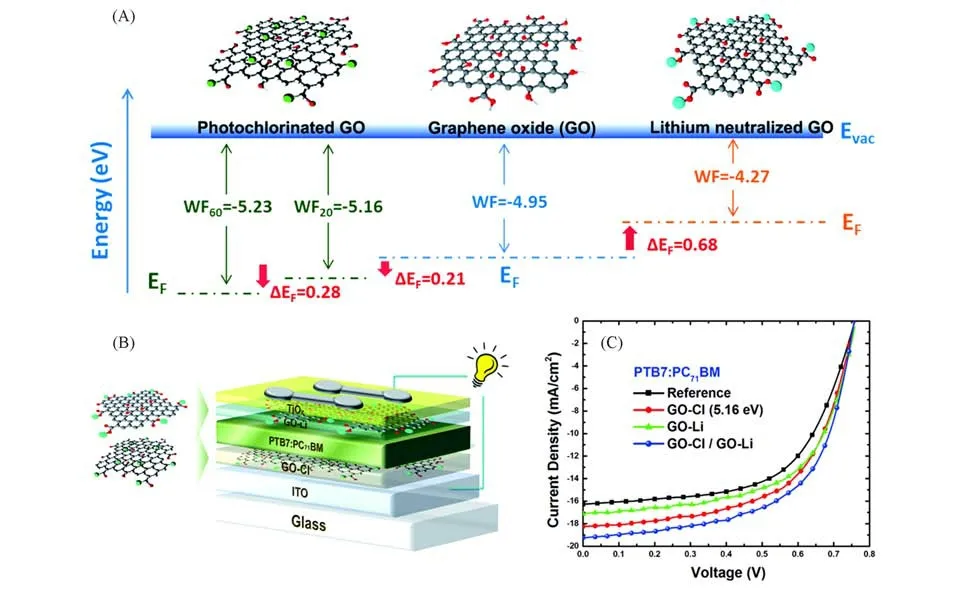
Fig.6 Tuning the energy band of GO by chemical dopping and its performance on organic solar cells[130]
4.1.4 Graphene and Its Derivatives as ETL or HTL Barrier Layer for PSCs and OPVs
Interfaces between each layer component of PSCs and OPVs,especially the absorber/ETL and absorber/HTL interfaces,play a pivotal role in achieving high-efficiency solar cells.Therefore,interface engineering is widely adopted to boost both the photovoltaic performance and stability of the devices by inserting an interlayer between the absorber layer and the transport layer.The roles of interface engineering mainly refer to:(1)pro⁃viding better charge selectivity and fast charge transfer/transport,and thereby suppressed electron-hole recom⁃bination[140—144];(2)forming well-aligned energy levels and imparting a cascade charge transfer for decreased energy loss[102,145];(3)improving the wettability of the subsequently deposited layer and thus increasing the quality of the films[146,147];(4)increasing the long-term stability of the device by blocking the penetration of the moisture into the active layer[139,142—145].By doping mesoporous TiO2(m-TiO2)with graphene flakes and simulta⁃neously inserting lithium-neutralized GO(GO-Li)flakes as interlayer at the m-TiO2/perovskite interface,Agrestiet al.[143]achieved a high PCE of 12.6% for large-area(active area of 50.6 cm2)PSCs modules,with fill factor(FF)increased from 95.4% to 64.6%[Fig.7(A),(B)].Zhaoet al.[144]also obtained high-perfor⁃mance PSCs with a PCE of 20.2% and an FF of 82% by using a chemically modified graphene/SnO2based ETL.Menget al.[145]inserted edge-enriched graphene nanoribbons at the TiO2/perovskite interface,which re⁃sulted in well-aligned energy levels for fast cascade charge transfer at the perovskite/ETL/FTO interfaces and also improved charge carrier conductivity[Fig.7(C),(D)],enabling a PCE increment from 15.87% to 17.69%.

Fig.7 Chemical doped GO and its performance in perovskite solar cells
4.2 Black Phosphorous as ETL or HTL for PSCs and OPVs
Phosphorus is an earth-abundant element and has three main allotropes,including red phosphorus(RP),white phosphorus(WP),and black phosphorus(BP).In contrast to WP and RP,BP is the most thermodynamically stable allotrope and is also nonflammable and insoluble in most solvent[148,149].As a new member of the 2D materials family,BP has also recently shown great promise in the application for electronic and optoelec⁃tronic devices and solar cells due to their fascinating physical and structural properties,such as finite band⁃gap,high ambipolar carrier mobility and large on-off current ratios[148—150].
In contrast to the graphene with zero bandgap,phosphorene sheet has a direct bandgap that can be effec⁃tively tuned in various approaches[148].Firstly,according to both density functional theory and experimental re⁃sults,the bandgap of BP correlates linearly to the inverse of the layer number of phosphorene,e.g.,1.6 eV for monolayer phosphorene,1.08 eV for bilayer phosphorene,0.74 eV for trilayer phosphorene and 0.40 eV for bulk BP[149—152].In addition to layer number,the bandgap can also be manipulated by the rotation angles be⁃tween the phosphorene sheets,the strain,the external electrical field,the functional groups,and so on[148].Moreover,BP has an ambipolar carrier mobility feature,and theoretical studies predicted an asymmetry and anisotropy for effective electron mass and mobility,i.e.,0.17m0for 1140 cm2·V−1·s−1in thex-direction and 1.12m0(m0is effective electron mass)for 80 cm2·V−1·s−1in they-direction.In the case of holes,the effective mass of the hole and its mobility are 0.15m0and 700 cm2·V−1·s−1in thex-axis,respectively,and 6.35m0and 26000 cm2·V−1·s−1in they-axis,respectively[148,149,151].Besides widely applications in electronic and optoelec⁃tronic devices,the ease of bandgap tunability and extraordinary charge carrier mobility is significant for the separation and transport of electrons and holes,which renders BP a promising choice as ETL and HTL materials for solar cells[148—160].
4.2.1 Black Phosphorous as HTL or Interlayer for PSCs and OPVs
Due to the extremely small deformation potential(0.15 eV),the monolayer phosphorene shows a holedominant transport[151,157].Therefore,BP was first exploited as hole transport materials for photovoltaics.In 2017,Chenet al.[158]synthesized BP quantum dots(BPQDs)in isopropanol by liquid exfoliation,the obtained BPQDs possess an optical band gap of 2.25 eV,a conduction band minimum(CBM)of−2.65 eV,and a va⁃lence band maximum(VBM)of−5.2 eV.When the BPQDs were deposited on PEDOT∶PSS layer and ser⁃viced as hole extractor for inverted p-i-n planar PSC device configured as“ITO/PEDOT∶PSS/BPQD/perovskite/PCBM/ZrAcAc/Ag,the resultant device yielded an improved efficiency ramping up from 14.1% to 16.7%(Fig.8).It was found that the fast hole extraction and suppression of recombination loss at the anode interface account for this remarkable enhancement in PCE[158].When BP nanosheets with a VBM of−5.2 eV were exclu⁃sively utilized as an HTM,Muduliet al.[159],gained a PCE of 7.88%for CH3NH3PbI3based PSCs;while the BP nanosheets were deposited as an interlayer between Spiro-OMeTAD and perovskite film,an efficiency of 16.4% was achieved,corresponding to aca.25% improvement as compared to Spiro-OMeTAD HTL only based devices.Zhaoet al.[160]integrated the BPs into the active layer of the benchmark polymer donor PTB7-Th and PC71BM acceptor,the bulk heterojunction organic solar cells yielded an impressive FF of 74.2%and a high PCE of 10.5%.Even though BP did not serve as HTL directly,they found that the inclusion of BP into active layer facilitated better carrier extraction and suppressed recombination[160].
4.2.2 Black Phosphorous as ETL or Interlayer for PSCs and OPVs
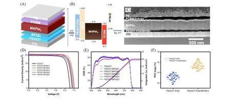
Fig.8 BPQD as hole transport material in perovskite solar cells[158]

Fig.9 BPQD as electron transport materials for organic solar cell and perovskite solar cell
Besides acting as HTL materials for solar cells,the ambipolar feature of BP provides itself the ability to serve also as electron transport materials for OPVs and PSCs.Our previous work demonstrated that the PCE of BP-incorporated OPVs enhanced by 11%in relative and an average PCE of 8.18%was gained when the solu⁃tion-processed BP flakes were coated on ZnO for three times and exploited as co-ETL.The CBM of BP films prepared with twice and three times coating were tested to be−4.06 and 3.86 eV,respectively.The formation of a cascaded band structure in the BP-incorporated devices with proper BP thickness facilitated the electron transport and thus enhanced the PCE of the solar cells[Fig.9(A),(B)][161].Additionally,we found in our later work that the fine BPQDs can also act alone as ETL for PSCs.The obtained flexible PSCs with BPQDs based ETL demonstrated a PCE of 11.26%[Fig.9(C),(D)][7].The 3.15-fold enhancement in efficiency arose from both the efficient electron extraction and suppressed non-radiative recombination compared with the devices built on the bare ITO surface without an ETL[7].By using a BP flakes+TiO2bilayer ETL,Batmunkhet al.[162]also improved the PCE of PSCs from 14.3%to 16.5%recently,due to the high carrier mobility and suitable band energy alignment with phosphorene inclusion.
In the above-mentioned studies,the BP or BPQDs have been exploited solely as either ETL(or interlayer at ETL/absorber interface)or HTL(or interlayer at HTL/absorber interface)for OPVs and PSCs.Nonethe⁃less,BP has a thickness-dependent,tunable direct bandgap and the conduction and valence bands of BP nanoflakes are also highly tunable through controlling their thickness.To this end,the simultaneous imple⁃mentation of BP with proper thickness at the respective interface in PSCs or OPVs may lead to synchronic en⁃hancement of charge extraction and collection at both HTL/absorber and ETL/absorber interfaces,thus remark⁃ably boosting the efficiency of the resulting solar cells.Most recently,Zhanget al.[163]developed a judicious design and incorporation of BP with optimized thickness to enhance carrier extraction at both ETL/perovskite and HTL/perovskite interfaces for high-efficiency PSCs.The resulting device delivered a progressively en⁃hanced PCE from 16.95%(BP-free)to 19.83%,which is resulted from the formation of synergy band energy alignment and thus concerted cascade interfacial carrier extraction,enhanced light absorption,and reduced trap density as well.Similarly,Wanget al.[164]used BPQDs as an interlayer to modify both the ETL and HTL film in PTB7-Th:FOIC blend based OPVs.They also found that the incorporation of BPQDs is beneficial to the formation of cascade band structure and fasten the electron/hole extraction,leading to a PCE enhancement from 11.8% to 13.1%.These works demonstrate that well-tailored BP with appealing characteristics is a promising transport material for solar cells and other optoelectronic devices.
4.3 Antimonene as ETL or HTL for PSCs and OPVs
As a group 15 element,antimonene,a new staring 2D materials,exhibits properties similar to those of BP,namely high carrier mobility and tunable bandgap.In contrast to BP,which is extremely sensitive to its surroundings and readily degrades when exposed to water and O2,antimonene shows better stability due to its buckled honeycomb structure with much stronger spin-orbital coupling(SOC)[165,166].The theoretical studies predicted that the bandgap of antimonene could be tuned in a wide range from 0 to 2.28 eV[165—167].In view of its bandgap tunability and stability,antimonene has been attracting increasing attention for various applica⁃tion,since it was first reported in 2015[165,167].
So far,Songet al.[168—170]has led researches on antimonene as charge transport materials for PSCs.In 2018,Songet al.[168]obtained smooth and larger antimonene nanosheets with tailored thickness from 0.5 nm to 7 nm and thus a tunable bandgap from 1.44 eV to 0.80 eV,by using a mortar pregrinding and subsequent sonication-assisted liquid-phase exfoliation process.When employed as HTL for CH3NH3PbI3based PSCs,the photocurrent density of the device was improved by about 30%due to the enhanced hole extraction,compared with the solar cells without HTL(Fig.10)[168].In the same year,they prepared semiconductor antimonene nanosheets with an indirect photoluminescence bandgap of 2.33 eV.When the antimonene was exploited as interlayer between perovskite/PTAA-HTL{PTAA=poly[bis(4-phenyl)(2,4,6-trimethylphenyl)-amine]},the antimonene-incorporated PSCs gained a PCE increment from 17.6% to 20.1% due to fast hole extraction[169].Later,they spread the antimonene oxide quantum dots(AOQDs)on the copper doped nickel oxide(Cu:NiOx)based HTL and found that the AOQDs can form a good energy level alignment between perovskite and Cu:NiOx-HTL for enhanced hole transfer.The resulting PSCs yielded an improved PCE form 15.7% to 18%[170].Wanget al.[171]deposited the soluble antimonene quantum sheets(AMQSs)on CuSCN to prepare a bilayer HTL.They found that the AMQSs can help to passivate the surface defects of CuSCN and diminish the recom⁃bination loss,leding a 12% enhancement in PCE(7.86%vs.8.8%)for PTB7-Th:PC71BM based OPVs as compared to the reference cell fabricated with pure CuSCN as an HTL.Zhaoet al.[172]incorporated the AMQSs(1.0 mg/mL)into the light absorber of OPVs,the obtained devices shows the highest PCE of 9.75% due to the enhanced light absorption,improved exciton dissociation,and reduced charge recombination,corresponding toca.25% enhancement in efficiency.Even though the theoretical results have predicted the appealing properties of antimonene,its practical applications are still limited so far.The great challenge remains on pre⁃paring high-quality antimonene due to the strong binding energy and ultrashort layer distance of the Sb crys⁃tal[167].
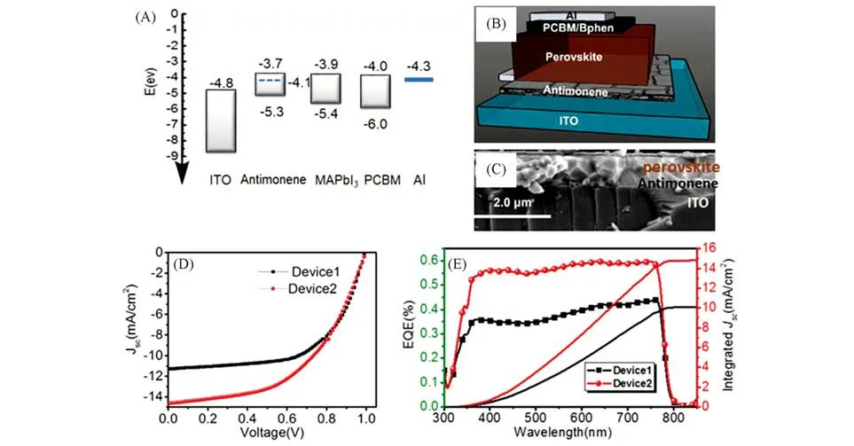
Fig.10 Antimonene as electron transport materials for perovskite solar cells[168]
4.4 Bismuthene as Charge Transport Materials for PSCs and OPVs
As another Group 15 2D material,bismuthene(Bi)has also received tremendous research interest due to its extraordinary optical and electronic properties similar to other members(namely phosphorene,arsenene,antimonene),such as high mobility and tunable bandgap.Bismuthene has semi-metallic characteristics,with a layer-dependent bandgap ranging from 0 eV for bulk to 0.54 eV for the monolayer structures[173—175].The car⁃rier mobility of Bi is as high as 5.7×106cm2·V−1·s−1(in bulk),which can enable ultrafast charge transfer for electronic and optoelectronic devices[173—176].In 2019,Wanget al.[176]built a 0D/2D nanohybrid by integrating a 0D CsPbBr3with 2D bismuthene nanosheets.The time-resolved photoluminescence and transient absorption spectroscopy measurements confirmed an ultrafast charge transfer process at the interface of the Bi/CsPbBr3heterojunction.Such a tunable charge transfer system has potential practical applications in devices such as photovoltaics and photodetectors.Most recently,Wanget al.[177]prepared a bismuthene-SnO2nanoparticle blend film as ETL for PSCs.They found that the inclusion of bismuthene could make the composite film smoother and more transparent and endowed higher crystallinity to the upper perovskite film.Moreover,the energy band of the bismuthene-SnO2composite layer was upshifted and the interfacial resistance between the composite layer and the perovskite layer was reduced,which resulted in accelerated electron extraction com⁃pared with pure SnO2-ETL based device.As a result,the resultant device gained an impressive PCE improve⁃ment from 17.35%to 18.75%.
5 Conclusions and Outlook
In summary,the uses of elemental 2D materials in solar cells have been demonstrated to be very effective in mastering efficiency and stability of PSCs and OPVs.They are very sensitive to broadband incident light(ex⁃cept for graphene),which enables more light absorption and potentially improve the efficiency of solar cells.Meanwhile,the incoperation of elemental 2D materials into solar cells can enhance the charge transfer,in⁃crease mobility,improve band alignment,tune work-function and limit ion diffusion,and further increase their energy conversion efficiency.At the same time,the availability and processability of the elemental 2D materials are also beneficial for higher efficiency and better stability,particularly making it feasible to adopt conventional large area printing processes for the development of stable PSCs’and OPVs’technology.However,it should be noted here that scalable production of elemental 2D materials is still a key issue for fabricat⁃ing large-area,high-efficiency solar cells.Moreover,some elemental 2D materials like BP still suffer from degradation in the air.So,how to prepare air-stable,uniform and broadband elemental 2D materials is still a big challenge for fabricating high-performce elemental 2D materials based solar cells.
Last but not least,other unstudied elemental 2D materials such as Te(tellurium)and Se(selenium)as shown in Fig.2,could also be synthesized and potentially find their applications in photovoltaics.As the mate⁃rial research community turns its attention to gain deep insight into the mechanism of the remarkable impact of elemental 2D materials on the performance of solar cells,more and more elemental 2D materials will be discovered(or re-discovered)in the foreseeable future.Due to their diverse properties and mono-elemental nature,elemental 2D materials can certainly occupy a special place in the 2D materials’family and eventually find a possible way going straight for industrial production.
This work is supported by the National Natural Science Foundation of China(No.61604058),the Shen⁃zhen Nanshan District Pilotage Team Program,China(No.LHTD20170006),the Science and Technology Pro⁃gram of Guangzhou,China(No.201904010212)and the Starting Research Funds from Songshan Lake Materials Laboratory,China(No.Y0D1051F211).
