Gallium-incorporated zinc oxide films deposited by magnetron sputtering and its microstructural properties
2021-02-02GUJinhuaZHUYaKANGHuai
GU Jinhua,ZHU Ya,KANG Huai
(1 Experimental Teaching and Laboratory Management Center,South-Central University for Nationalities,Wuhan 430074,China; 2 Hubei Key Laboratory of Intelligent Wireless Communication,South-Central University for Nationalities,Wuhan 430074,China; 3 College of Electronic Information Engineering,South-Central University for Nationalities,Wuhan 430074,China)
Abstract Transparent conductive gallium-doped zinc oxide thin films were deposited by magnetron sputtering technique onto glass substrates.The crystallinity and microstructural properties of the deposited samples were investigated by means of X-ray diffractometer and quantitative analysis.The results show that all the samples are polycrystalline with a hexagonal wurtzite structure and grow preferentially in the(002) direction.The microstructure parameters such as lattice constants,interplanar spacing and Zn-O bond length were determined and the results are in agreement with that of the standard ZnO.When the film thickness is 570 nm,the deposited sample exhibits the best crystal quality and microstructural properties,with the maximum(002) texture coefficient and mean crystal size,and the minimum lattice strain and dislocation density.
Keywords magnetron sputtering; doped zinc oxide; thin film; microstructure
Gallium-incorporated zinc oxide(ZnO) is a highly promising transparent semiconductor material for applications as transparent conducting electrodes in thin film transistors[1-2],liquid crystal displays[3],organic light-emitting devices[4-7],photovoltaic solar cells[8-10],gas sensors[11-12]and surface acoustic wave devices[13].Compared with tin-doped indium oxide thin films,the gallium-incorporated ZnO thin films have a variety of advantages such as wide direct bandgap(3.3 eV),high exciton binding energy(60 meV),low material cost and environmental friendliness,apart from high optical transmittance in the visible region and high electrical conductivity,The ZnO-based thin films can be fabricated using different preparation techniques[14-25],such as chemical vapour deposition,radio frequency magnetron sputtering,direct current magnetron sputtering,electron beam evaporation,pulsed laser ablation,sol-gel process,atomic layer deposition,spray pyrolysis,etc.Among these deposition methods,the radio frequency magnetron sputtering is considered to be a suitable technique due to its advantages such as high deposition speed,low cost,easy control of deposition parameters and simplicity of the deposition system required[26-28].In the present study,the gallium-incorporated ZnO thin films were deposited on glass substrates by radio frequency magnetron sputtering technique,and the effect of film thickness(t) on the crystalline quality and microstructural properties of the deposited samples were investigated in detail.
1 Experiment
The gallium-incorporated ZnO thin films were deposited onto the glass substrates by radio frequency magnetron sputtering system(MS-560C) using a ZnO doped 3 wt% Ga2O3target with a base pressure of 4.5×10⁻⁴Pa.The distance between the target and the glass substrate was 75 mm,and high-purity argon gas(purity of 99.999 %) was used as the working gas.The deposition parameters of temperature,power and argon pressure were 290 ℃,170 W and 0.5 Pa,respectively.The film thicknesstof the samples was controlled to be in the range of 400 nm and 1000 nm by adjusting the sputtering time during the deposition.Thetvalue was measured by a stylus surface roughness detector(Alpha-step 200).In this paper,for the samples with thicknesstof 410 nm,570 nm,750 nm and 980 nm are labelled as sample 1(S1),sample 2(S2),sample 3(S3) and sample 4(S4),respectively.
XRD patterns of the samples were obtained with a Bruker D8 Advance model X-ray diffractometer using Ni-filtered Cu Kαradiation(λ=0.15406 nm) at room temperature.The diffractograms were recorded from 10° to 80° with 0.016° steps.Crystallite phases were determined by comparing the diffraction patterns with those in the standard powder XRD files(JCPDS) published by the International Center for Diffraction Data.
2 Results and discussion
Figure 1 presents the XRD patterns of all the deposited thin films.For all the samples,the diffraction peak positions of 2θlocated at about 31°,34° and 72° are associated with the(100),(002) and(004) plane of hexagonal phase according to the JCPDS card No.36-1451(ZnO)[29,30].Note that all the samples possess the polycrystalline character with hexagonal wurtzite structure.No other phase such as gallium and gallium oxide can be detected in the prepared thin films,which indicates that the gallium ions entering the crystal lattice of zinc oxide,creating the ZnO solid solution.Eshaghi et al.[31]and Chen et al.[32]reported similar results in aluminum-incorporated ZnO and titanium-incorporated ZnO thin films.From
Figure 1,it is seen that the intensity of(002) peak is much stronger than the others for all the samples.The result implies that all the deposited thin films have hexagonal wurtzite structure with highlyc-axis orientation.
The preferred orientation of the deposited samples was evaluated by the texture coefficientTC(hkl)using the following formula[33-34]:
(1)
where the subscriptsh,kandlare Miller indices,I(hkl)is the X-ray diffraction intensities obtained from the prepared thin films,I0(hkl)is the standard intensity of JCPDS card No.36-1451,andNis the number of diffraction peaks considered.Figure 2 displays the values ofTC(100),TC(002)andTC(004)for the deposited samples.From the
Figure,it is found that the maximumTC(hkl)values are in(002) plane for all the deposited thin films,which indicates that the maximum preferred orientation of all the samples along the(002) diffraction plane.As shown in the
Figure 2(b),theTC(002)is also observed to increase initially and then decrease with the increase of the thicknesst.Clearly,the sample S2 has the highestTC(002)value of 2.958,suggesting that the best(002) preferred orientation of the thin film can be obtained whent=570 nm.
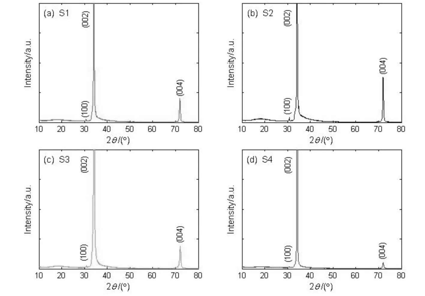
Fig.1 XRD patterns of all the deposited samples图1 所有沉积样品的XRD图谱

Fig.2 The values of TC(100),TC(002) and TC(004) for all the deposited samples图2 所有样品的织构系数TC(100),TC(002)和 TC(004)数值
Figure 3 shows the full-width at half-maximum(FWHM) values of(002) peak of all the deposited thin films.As can be seen,theFWHMfalls firstly and then rises with the increase of thicknesst,and the minimumFWHMof 0.083° can be obtained whent=570 nm.The decrease of theFWHMimplies the increase of mean crystal size(Cs) of the deposited films.TheCsvalues of the samples can be calculated fromFWHMdata according to the Debye-Scherrer equation[35]:
(2)
whereKis the shape factor,possessing a numerical value of 0.9;λis the wavelength of the XRD measurement used;FWHMis the full width at half maximum of the measured(002) peak in radians; andθis the Bragg diffraction angle.The lattice strain(ε) and dislocation density(δ) can be estimated from the following formulae[36]:
(3)
(4)
The values ofCs,εandδof all the deposited samples were calculated and are plotted in
Figure 4.As the thicknesstincreases,the crystal sizeCsincreases initially and thereafter decreases,while the lattice strainεand dislocation densityδexhibit the reverse variation trend.When thicknesst=570 nm,the deposited sample possesses the best crystalline and microstructural properties,with the narrowestFWHMof 0.083°,the largestCsof 98.8 nm,the lowestεof 3.51×10⁻⁴and the minimumδof 1.02×10¹⁴m-2.The results suggest that the crystal quality of the prepared thin films is strongly dependent upon the thicknesst.

Fig.3 The FMWH values of(002) peak for all the deposited samples图3 所有沉积样品(002)衍射峰的FMWH数值

Fig.4 The values of Cs, ε and δ for all the deposited samples图4 所有沉积样品的Cs, ε 和 δ 数值
The lattice constants of the deposited films were calculated from XRD data using the following equations[37-38]:
(5)
2d(hkl)sinθ=λ,
(6)

The Zn-O bond length(L) was estimated using the relation[39]:
(7)
whereuis a positional parameter.For wurtzite structureuis expressed as[39]:
(8)
The calculated values ofa,candc/aratio for all the deposited thin films are plotted in
Figure 5.

Fig.5 The values of a,c and c/a for all the deposited samples图5 所有沉积样品的a,c和c/a数值
As can be seen,the lattice constantais found in the range of 0.33423-0.33542 nm,cis in the range of 0.52351-0.52474 nm,andc/ais in the range of 1.56442-1.56629.The standard JCPDS data of ZnO having hexagonal wurtzite structure provides the lattice constant values asa=0.32498 nm,c=0.52066 nm,d=0.26033 nm andc/a=1.6021(JCPDS card No.36-1451).Clearly,the values of lattice constants are found to slightly vary with thicknesst.
Figure 6 shows the calculated values ofdandLfor all the deposited thin films.The ionic radius of O2-being 0.138 nm and of Zn2+being 0.072 nm,the covalent bond length of Zn-O should ideally beL=0.210 nm.From the
Figure,the bond lengthLis observed in the range of 0.20201-0.20265 nm whereasdis in the range of 0.26176-0.262373 nm.No significant change in the interplanar spacing and Zn-O bond length is observed after doping for all the deposited samples.

Fig.6 The values ofd and L for all the deposited samples图6 所有沉积样品的d和L数值
3 Conclusions
The gallium-incorporated ZnO samples were deposited onto the glass substrates by applying radio frequency magnetron sputtering technique.The crystalline quality and microstructural characteristics of the deposited samples were investigated by applying X-ray diffractometer.Based on the measured XRD data of the samples,the microstructure parameters such as the lattice constants,the interplanar spacing and the Zn-O bond length were determined.The XRD studies indicate that all of the deposited samples are polycrystalline with a hexagonal wurtzite structure and grow preferentially in the(002) direction.The obtained values of lattice constants,interplanar spacing and Zn-O bond length are in agreement with that of the standard ZnO.The deposited sample with the film thickness of 570 nm has the best crystallite quality and microstructural properties,with the highest texture coefficient of(002) plane,the narrowest full width at half-maximum,the largest mean crystal size,the lowest lattice strain and the minimum dislocation density.
