L-DSP片上调试电路的设计与实现
2020-12-21白创李帆汪东
白创 李帆 汪东
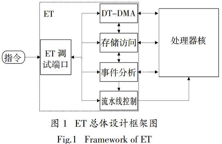
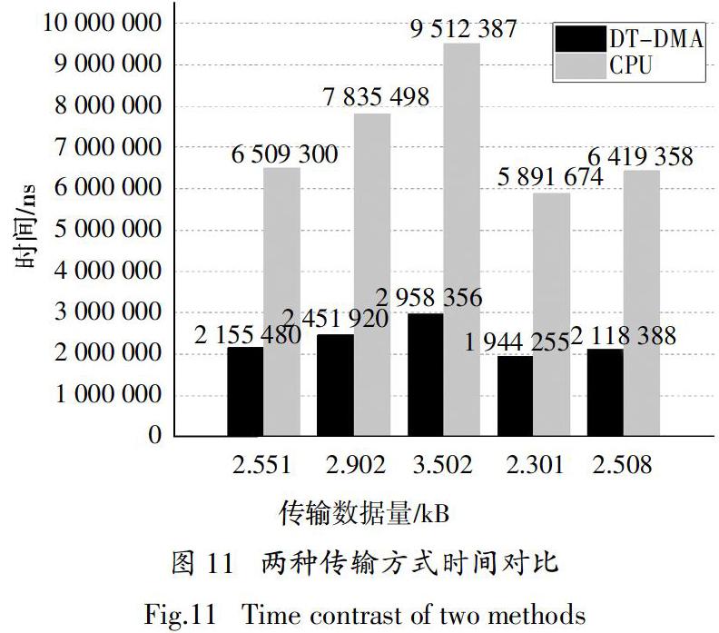
摘 要:针对L-DSP的调试需求,设计了一种基于JTAG接口的片上调试电路.该调试电路实现了存储资源访问、CPU流水线控制、硬件断点/观察点、参数统计等调试功能.相对于传统调试方式,本文电路通过增加DT-DMA模块,实现数据在外设与内存之间直接传输,极大地提升了调试效率.调试电路在0.18 μm CMOS工艺下实现,面积为167 234.76 μm2,功耗为8.89 mW.同时,调试电路与L-DSP全芯片在FPGA下进行验证,结果表明,该调试电路调试功能完整且DT-DMA传输调试数据的速度是CPU传输的3倍.
关键词:调试;片上调试;JTAG接口;DT-DMA;DMA操作
中图分类号:TN495 文献标志码:A 文章编号:1674—2974(2020)08—0069—05
Abstract:According to the debug requirements of L-DSP, an on-chip debug circuit based on JTAG interface is proposed in this paper, which implements the debug functions such as storage resource access, CPU pipeline control, hardware breakpoint/observation point, and parameter statistics. Compared with the traditional debug mode, the proposed debug circuit realizes the direct transmission of data between peripherals and memory by adding a DT-DMA module, which greatly improves the debug efficiency. The proposed circuit is designed in a 0.18 μm CMOS process with an area of 167 234.76 μm2 and a power consumption of 8.89 mW. And the proposed circuit and L-DSP are verified under the FPGA. The results show that the proposed circuit has complete debug functions and the rate of DT-DMA for transferring debug data is three times faster than that of the CPU.
Key words:debugging;on-chip debug;JTAG interface;DT-DMA;DMA operation
随着半导体制造工艺的不断进步,芯片的集成度越来越高,实现的功能越来越复杂,使得芯片正确性调试与故障定位的需求难以得到保证[1]. 同时芯片的快速市场化又使得其研发周期越来越短. 因此,可靠的调试手段显得尤为重要,准确、快速的调试方法直接影响到芯片的开发效率与进度[2].
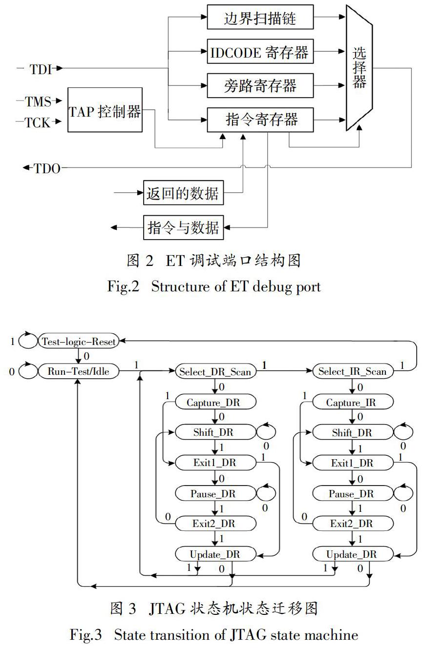
根据通信接口的不同,常用片上调试方法包括基于串口通信、基于BDM接口和基于JTAG接口3种调试方法.基于串口通信的调试方法,其功能虽然完善,调试过程也十分简便[3],但因其占用芯片一些引脚资源,存在无法进行自我调试等弊端,使得该方法在某些场合并不适用[4-5]. 而基于BDM接口的片上调试技术虽然被业界广泛使用[6],但是没有相关协议支持边界扫描功能,需要开发者自行承担风险.基于JTAG接口的调试方法是目前包含军事领域在内大部分芯片采用的……