Electronic structure of single-crystalline graphene grown on Cu/Ni(111)alloy film∗
2019-08-16XueFuZhang张学富ZhongHaoLiu刘中灏WanLingLiu刘万领XiangLeLu卢祥乐ZhuoJunLi李卓君QingKaiYu于庆凯DaWeiShen沈大伟andXiaoMingXie谢晓明
Xue-Fu Zhang(张学富), Zhong-Hao Liu(刘中灏), Wan-Ling Liu(刘万领), Xiang-Le Lu(卢祥乐),Zhuo-Jun Li(李卓君),4, Qing-Kai Yu(于庆凯),4, Da-Wei Shen(沈大伟),4,‡, and Xiao-Ming Xie(谢晓明),2,,4
1State Key Laboratory of Functional Materials for Informatics,Shanghai Institute of Microsystem and Information Technology(SIMIT),Chinese Academy of Sciences,Shanghai 200050,China
2University of Chinese Academy of Sciences,Beijing 100049,China
3School of Physical Science and Technology,Shanghai Tech University,Shanghai 200031,China
4CAS Center for Excellence in Superconducting Electronics(CENSE),Shanghai 200050,China
Keywords: single-crystal graphene,electronic structure,Cu/Ni(111)
1. Introduction
Graphene is well studied as a two-dimensional(2D)material with fantastic physical properties such as high carrier mobility,atomically thin thickness,and ultra-high mechanical strength,which make it a potential candidate for versatile applications, especially for microelectronics.[1-9]The synthesis of large-size single-crystal graphene(SCG)film is highly desired for electronic applications.One can produce high-quality and large-size SCG by epitaxial growth on various substrates such as Cu(111)through highly oriented islands of graphene seamlessly into an SCG.[10-13]For epitaxial graphene grown on the substrates with different lattice constants and interface energies, the substrates have a significant effect on both growth conditions and electronic structures of graphene.[14-25]Upon interaction with the underlying substrate,the electronic structure of graphene would efficiently change,e.g.,resulting in band gap at Dirac point.[16,26-30]Actually, different band gaps of graphene on various substrates have been reported by angle-resolved photoemission spectroscopy(ARPES),[16,26,30]which indicate that the substrates have an important influence on the electronic structural properties of graphene.
In this work, we have successfully grown high-quality SCG by chemical vapor deposition (CVD) on a novel substrate Cu/Ni(111)thin film,with a growth temperature lower than that on other conventional substrate. The low growth temperature not only decreases the energy consumption, but also solves a variety of problems, including high contamination, metal evaporation, and wrinkles owing to the mismatch of thermal expansion coefficients between the substrate and graphene. By means of ARPES,we systematically investigate the electronic structure of single-crystalline graphene grown on Cu/Ni (111), which has been characterized before by optical imaging (OM), scanning electron microscopy (SEM),atomic force microscope (AFM), Raman spectroscopy, and low energy electron diffraction (LEED). We find that the graphene grown on Cu/Ni(111)has the high crystallinity and the robustness of the Dirac cone-like electronic structure. The Dirac band crossing at the binding energy of 304 meV opens a gap of approximately 152 meV,which is supposed to be induced by the interaction with the substrate.
2. Experiment
SCG was acquired by CVD on Cu/Ni (111) thin film at 750°C with 300-sccm Ar, 20-sccm H2, and 50-sccm CH4(0.5% diluted in Ar) for 50 min for pretreatment at atmospheric pressure. The source of Cu/Ni alloy contains 85%Cu and 15% Ni. Subsequently, the sample was rapidly cooled under the same gas flow. To characterize graphene by Raman spectra,the as-grown graphene film was transferred onto SiO2/Si substrate by the poly(methyl methacrylate)(PMMA)-assisted method. Graphene film was spin-coated with PMMA and baked at 50°C for 10 min. Then, a 1-mol·L-1Na2S2O8solution was used to etch the Ni/Cu film away. After being rinsed by deionized water, the PMMA/graphene was subsequently washed by isopropanol and then dried in air for 10 min before it was placed onto the SiO2/Si substrate. Subsequently,the PMMA was dissolved by acetone.
ARPES measurements were performed at the dream-line and 03 U beamline of Shanghai Synchrotron Radiation Facility (SSRF). The energy and angular resolutions were set to 15 meV and 0.2°,respectively. The samples were heated from room temperature to 300°C and then kept at 300°C for 6 hours in the ultra-high vacuum (UHV) chamber to clean the surfaces before measurements. During the measurements,the temperature was kept at 30 K and the pressure was maintained greater than 5×10-11Torr(1 Torr=1.33322×10⁵Pa).
3. Results and discussion
The substrate of Cu/Ni (111) alloy film is characterized by a scanning electron microscope, electron backscattering diffraction(EBSD),and x-ray diffraction(XRD),respectively,as shown in Fig.1. The SEM image(Fig.1(a))illustrates the ultra-flat substrate without grain-boundary. In order to check the crystallinity of the Cu/Ni thin film,we have carried out the EBSD mapping. As shown in Fig. 1(b), the EBSD pole image of Cu/Ni film shows three evenly distributed points,which indicates the single-crystal Cu/Ni film without in-plane twin structures.[12]The XRD characterization (2θ scan) indicates an out-of-plane (111) orientation of the face-centered-cubic Cu/Ni alloy thin film (Fig. 1(c)). The lattice constant of the substrate is 0.363 nm, which is close to the lattice constant of Cu substrate (0.361 nm). Additionally, a φ scan is conducted by rotating the sample normal to the surface with highresolution XRD. As shown in Fig. 1(d), the diffraction peaks of Cu/Ni film periodically appear at intervals of 120°with a very narrow full width at half-maximum of 0.3°. The 3-fold trigonal symmetry of single (111) pole also further supports the single crystalline nature of the Cu/Ni (111) film without in-plane twin structures.[10,12]Combining the EBSD and XRD results,we can confirm that the Cu/Ni alloy thin film is singlecrystalline with the(111)-oriented.

Fig.1. Characterization of the Cu/Ni(111)film. (a)SEM image of the morphology of Cu/Ni (111) thin film. (b) EBSD map of Cu/Ni (111) thin film.The inset shows the pole figure of Cu/Ni(111)thin film. (c)XRD pattern of Cu/Ni (111) film, showing the well-defined (111)-orientation out-of-plane.(d) High-resolution XRD azimuthal off-axis scan of Cu/Ni (111) in-plane orientation.
Graphene/Cu (111) has a lattice mismatch ratio of approximately 4%while that of graphene/Ni(111)is only 1.2%.Comparing to Cu(111),Ni(111)has a stronger catalytic ability to decompose methane. Figure 2 shows the manufacturing process of single-crystal graphene on Cu/Ni (111) substrate by CVD. Cu/Ni (111) thin film is fabricated firstly on Al2O3(0001) for epitaxy of graphene. The nucleation of grapheme is deposited on Cu/Ni(111)with identical orientation because of the regulation of single-crystal substrate. Then graphene domains seamlessly stitched and formed a single crystal.
Figures 3(a)-3(c) show the ultra-flat wrinkle-free graphene film grown on Cu/Ni(111)characterized by the OM,SEM, and AFM, respectively. Figure 3(d) shows the OM of graphene transferred on a Si substrate covered by 300-nm SiO2. The representative Raman spectra of transferred graphene are taken randomly, as shown in Fig.3(e). Without D peak of the graphene,the intensity ratio of 2D/G band is homogeneously larger than 2,indicating high-quality monolayer graphene. The LEED measurement is applied to investigate the crystallinity of graphene grown on Cu/Ni(111)alloy film.As shown in Fig.3(f),the LEED pattern of the graphene shows only one set of diffraction pattern with an aligned six-fold rotational symmetric spots arranged in a suitable honeycomb lattice,indicating single-crystal graphene with uniform size and orientation.
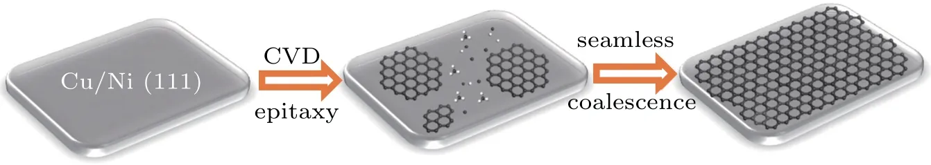
Fig.2. Schematic diagram of experimental design for growth of graphene on Cu/Ni(111).
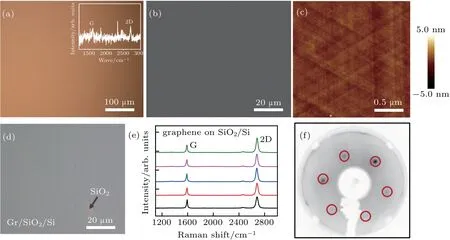
Fig.3. Investigation of graphene on Cu/Ni thin film. (a)Typical optical images of graphene covering on the Cu/Ni alloy thin film. Inset: Raman spectra of graphene grown on Cu/Ni. (b)The SEM morphology of graphene on Cu/Ni(111)thin film. (c)The AFM morphology of graphene grown on Cu/Ni(111)thin film. (d)Optical images of graphene transferred onto the SiO2/Si substrate. (e)Raman spectra of graphene taken randomly from panel(d). (f)LEED pattern of graphene on Cu/Ni(111).
We investigate the Fermi surface and the low-energy electronic structure of graphene grown on Cu/Ni (111) film by ARPES.As shown in Fig.4,the clear images of the Fermi surface and the dispersive bands are indicative of the high crystalline quality of the sample. Figure 4(a)shows the Fermi surface intensity plot,which is similar to that of graphene grown on Cu(111)substrate.[26]The bright spots at the K (K′)point are attributed to the spectra from the top graphene, while the redundant intensity should come from the substrate,i.e.,Cu-Ni sp bands. Estimating from the data, the value of the dis-tance from K to K′point is 1.72±0.02 ˚A-1, corresponding to the lattice constant of approximately 2.43 ˚A. Figure 4(b)shows the wide valence bands along Γ-K-K′direction near the Fermi level. One can clearly see the Dirac-like dispersions at the K and K′points,in which the π and σ bands come from the carbon,and the sp and d bands are from the substrate. To quantitatively study the Dirac-like dispersion,we zoom in the photoemission intensity plot around the K point, as shown in Fig. 4(c). Figures 4(d) and 4(f) show the corresponding momentum distribution curves (MDCs) and energy distribution curve (EDC) centered at the K point, respectively. By fitting the MDCs (Fig. 4(e)) and then extracting the dispersion, we can obtain that the Fermi velocity of the linear dispersion is approximately 1.1×10⁶m/s. The EDC indicates that a gap of approximately 152 meV opens at the binding energy of approximately 304 meV,the Dirac point. The gap size is smaller than that of graphene on Cu(111)which is about 250 meV at the binding energy of approximately 300 meV.[26]
The factors in the opening of the bandgap of graphene come from many aspects. It is generally believed that the decisive factor is symmetry breaking induced by the interaction with the substrate. There are two principal types of symmetry breaking resulting in the bandgap of graphene. One is the spatial inversion symmetry breaking, and the other is lattice translational symmetry breaking. Two sides of epitaxial graphene are, respectively, subjected to different interactions from the substrate and space,leading to spatial inversion symmetry breaking. Thus,the substrate-induced bandgap opens in epitaxial graphene. On the other hand,the crystal defect,such as wrinkles,atomic vacancies,and localized disorders,would break the translational symmetry.
The bandgap of graphene grown on Cu/Ni (111) is smaller than that of graphene on Cu (111), which indicates that the symmetry breaking induced by Cu/Ni(111)substrate is less than that in graphene/Cu (111). In addition, the slight difference between the carbon atoms on Cu and Ni atoms would break the translational symmetry and further affect the bandgap of graphene,which need to be further studied.
4. Conclusion
In summary,we have reported a new approach for the fabrication of ultra-flat single-crystal graphene on Cu/Ni(111)at 750°C, which is much lower than those of earlier reports on catalytic substrates. The energy-momentum dispersion measured by ARPES reveals the robustness of the Dirac-like dispersion. The gap sizes of Dirac-like band of graphene on different substrates have quantitative differences resulting from the interaction of the substrates, which might provide a suggestion to optimize the synthesis conditions for graphene. The relatively low growth temperature with the robust Dirac-like dispersion at the Fermi level suggests graphene on Cu/Ni(111)as a remarkable platform for studying and applying the novel physical properties related to Dirac fermions. In addition,by building relationship between the single-crystal graphene electronic structure and the parameters of the CVD methods,ARPES studies are able to provide the key information on the optimal synthesis conditions of the graphene and shed light on the electronic structure responsible of their chemical,physical,and transport behaviors.
猜你喜欢
杂志排行

Chinese Physics B的其它文章
- Lorentz transmission electron microscopy for magnetic skyrmions imaging∗
- Spin transport in antiferromagnetic insulators∗
- First-principles study of the band gap tuning and doping control in CdSexTe1-x alloy for high efficiency solar cell∗
- Non-Stokes drag coefficient in single-particle electrophoresis:New insights on a classical problem
- SymTopo: An automatic tool for calculating topological properties of nonmagnetic crystalline materials∗
- Tunable coupling between Xmon qubit and coplanar waveguide resonator∗