Suppression of Ambipolar Conduction in Schottky Barrier Carbon Nanotube Field Effect Transistors:Modeling,Optimization Using Particle Swarm Intelligence,and Fabrication
2019-06-12ReenaMonicaandSreedevi
P.Reena Monica and V.T.Sreedevi
Abstract: A mathematical model and experimental analysis of the impact of oxide thickness on the ambipolar conduction in Schottky Barrier Carbon Nanotubes(CNTs)Field Effect Transistor(SB CNTFETs)is presented.Suppression of ambipolar conduction in SB CNTFETs is imperative in order to establish them as the future of IC technology.The ambipolar nature of SB CNTFETs leads to a great amount of leakage current.Employing a gate oxide dielectric of thickness,tox~50 nm suppresses the ambipolar behavior.In an SB CNTFET,it is the electric field at the source/drain contacts that control the conductance and the band bending length at the contacts is defined by tox.Therefore,tox is the prime parameter that influences the width of the Schottky barrier and the current in the subthreshold region.Due to the wide SB,there is a loss in on-current due to tunneling,but the current due to thermionic emission is increased by employing a high-κ dielectric such as Zirconium dioxide(ZrO2).This work proposes an approach to suppress ambipolar behavior in SB CNTFETs without decreasing the on current.The thickness and dielectric constant of the gate oxide are optimized using the particle swarm optimization(PSO)algorithm to achieve suppression of ambipolar conduction without any loss in on-current.The proposed SB CNTFET was modeled using Verilog-A.Experimental demonstration of the suppression of ambipolar property is also presented.Two SB CNTFETs are fabricated using high-κ dielectric such as ZrO2 with different thickness.A device with thin(~5 nm)gate oxide and another device with thick(~50 nm)gate oxide were fabricated.From the experimental results,it is observed that the device with the thin gate oxide exhibited ambipolar characteristics and the device with the thick gate oxide did not exhibit ambipolar characteristics.The increase in thickness,tox,ensures suppression of ambipolar behavior.
Keywords: Ambipolar conduction,Carbon nanotubes,high-κ gate oxide,Schottky barrier.
1 Introduction
The emerging trend towards Internet of Things(IoT)has increased the demand for scaled down low power devices with high performance[Atzori,Iera and Morabito(2010)].The development in nanoelectronics with novel materials such as semiconducting carbon nanotubes(CNTs)addresses this need.CNTs exhibit excellent carrier mobility at nanoscale[Dürkop,Getty,Cobaset al.(2004)].They are capable of carrying high currents without scattering due to their ballistic electron transport[Zhang,Zhu,Wang et al.(2004)].The Carbon Nanotube field effect transistors(CNTFETs)are in the limelight among all novel nanoelectronic devices for their promising device characteristics[Avouris,Appenzeller,Martelet al.(2003)].The high-frequency characterization of CNTFETs up to 10 GHz was reported by Huo et al.[Huo,Zhang,Chan Philip et al.(2004)].In the recent years,CNTFETs are found in the IoT space in gas sensing,CNT based antennas and in RF interconnects[Xuan,Thuy,Luyen et al.(2017);Chen,Zhang,Feng et al.(2008);Liu,Chen,Zhang et al.(2009);Bhatt,Vijay,Joshi et al.(2017);Taghavi,Carta,Meister et al.(2017);Bayat,Ramin and Kashani-Nia(2017);Li,Tianjian,Jing et al.(2018)].CNTs have the potential to be used as the next-generation ultrasensitive gas sensors[Thai,Yang,DeJean et al.(2011)].Despite all these credentials,there are certain hurdles which limit the usage of CNTFETs.This paper addresses one such hurdle,i.e.,the ambipolar conduction which imposes a concern when the CNTFETs are stacked.Ambipolar behavior is not desirable as it increases the OFF state leakage current and degrades the performance of CNTFETs.The OFF current is due to the tunneling of holes through the Schottky Barrier(SB).Negative gate to source voltages will result in high leakage currents.A metal contacted CNTFET is preferred over a highly doped semiconductor contacted CNTFET because the metals have notably lower parasitic resistance[Javey and Kong(2009)].This work focuses on the metal contacted Schottky Barrier CNTFET(SB CNTFET).Earlier,the only solution to make the device unipolar was to dope the contacts heavily[Javey and Kong(2009)].Other effective ways of suppressing ambipolar behavior in SBCNTFET are demonstrated:Halo doping of the channel in CMOS technologies is one of the techniques to decrease short channel effects[Ieong,Narayanan,Singh et al.(2006);Hwang,Lee and Hwang(1996);Zanchetta,Todon,Abramo et al.(2002);Endoh and Momma(2007)].This technique is used in CNTFETs to suppress ambipolar behavior.For some particular length of the CNT channel,p-type dopants are added.Since the source side of the channel is p-doped,it is screened from all variations in the drain potential.It has been demonstrated[Zahra and Orouji.(2009)]that the leakage current can be lowered by the halo doping technique.Another novel device,a linear doped channel(LDC)CNTFET is presented by Naderi et al.[Naderi,Keshavarzi and Orouji(2011)].Instead of a halo doping on one end of the channel,the doping is linearly distributed throughout the channel with a maximum concentration at the source side decreasing linearly to zero as it goes to the drain side of the channel.The suppression of ambipolar behavior of CNTFETs can also be achieved by engineering the gate structure.A vertical partial gate where the gate covers only a part of the channel suppresses the ambipolar behavior[Yoon,Fodor and Guo(2008)].The absence of gate at the drain side makes the SB thick at this side ensuring unipolar behavior.A deep trench introduced under the CNT near the source or drain contact can also create the same impact of the gate not controlling the channel.The trench area under the CNT is not controlled by the back gate[Lin,Appenzeller and Avouris(2004)].Therefore the lack of control over that part of the channel makes the SB thick at the source/drain side,thus suppressing ambipolar behavior.All of these methods rely on sophisticated fabrication techniques.A much simpler solution is demonstrated by Guo et al.[Guo,Datta and Lundstrom(2004)].The impact of gate oxide thickness and the role of nanotube diameter are studied.The study revealed that the CNTFETs with thin gate oxide(4 nm)exhibited ambipolar characteristics[Guo,Datta and Lundstrom(2004)].The thickness of the SB is approximately the thickness of the gate oxide[Odintsov(2000)].The gate capacitance,Cox,in long channel devices is inversely proportional to the logarithm of the oxide thickness,tox,due to the one dimensional nature of the CNTs.Aggressive scaling of tox,makes the Schottky barrier thin which enables tunneling through the barrier and ambipolar conduction.In silicon MOSFET,the charge in the channel is affected by toxthrough the gate capacitance and thus affecting the conductance in the ON state.However,in an SB CNTFET,it is the electric field at the source/drain contacts that controls the conductance and the band bending length at the contacts is defined by tox.Therefore,toxis the prime parameter that influences the width of the Schottky barrier and the current in the subthreshold region[Odintsov(2000)].There are experimental results revealing the fact that CNTFETs with thin gate oxide has a tendency to be ambipolar with nearly symmetrical characteristics[Radosavljevic,Heinze,Tersoff et al.(2003)].A backgated SB CNTFET with 2 nm and 5 nm thick gate oxide exhibited ambipolar characteristics.When the gate insulator was thick(40 nm),an asymmetric barrier height led to asymmetric electron and hole conduction[Guo,Datta and Lundstrom(2004)].Thus the ambipolar behavior is suppressed by having a thick gate dielectric.
Thus it is important to get optimal values of gate oxide thickness to suppress the ambipolar conduction.Particle swarm intelligence based optimization is carried out to get the optimal gate oxide thickness in order to suppress the ambipolar conduction.
The result of the optimization suggested thick gate dielectric of 50 nm.Therefore,in this work,in order to suppress the ambipolar behavior,gate dielectric of thickness ~50 nm is employed.However,the thick gate dielectric reduces the on current due to tunneling.In order to compensate this reduction in on current,a high-κ dielectric such as zirconium dioxide(ZrO2)is used.Generally,high-κ dielectrics are used to reduce leakage current in scaled-down devices with thin gate oxides.The purpose of a high-κ dielectric in this work is to increase the conductance by thermionic emission.Thereby,the on-current is not affected.This proposed SB CNTFET is modeled and written in Verilog-A.In order to demonstrate the occurrence of ambipolar conduction in SB CNTFETs with CNTs as a channel and thin gate oxide,an SB CNTFET with tox≈5 nm was fabricated and characterized.Also,to demonstrate the suppression of ambipolar conduction in an SB CNTFET with thick gate oxide,an SB CNTFET with tox≈50 nm was fabricated and characterized.The results clearly indicate that the high-κ dielectric ensures better oncurrent when compared to the on-currents reported in the literature,where low-k dielectric such as SiO2is used[Javey,Guo,Wang et al.(2003)].The increase in thickness,tox,ensures suppression of ambipolar behavior.
This paper is organized as follows:Section 2 presents the mathematical model of the proposed SB CNTFET and the optimization using particle swarm intelligence.Section 3 presents the fabrication procedure followed in this work.The results and inferences are discussed in Section 4.Section 5 concludes the paper.
2 The model
2.1 Modeling the SB CNTFET
An SB CNTFET with a single-walled CNT as the channel exhibits ambipolar behavior.In the SB CNTFET model shown in Fig.1[Javey and Kong.(2009)],when the source side SB and the drain side SB are taken into account,the distribution functions as shown in Eq.(1)and Eq.(2)are derived.
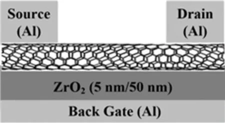
Figure 1:Cross-sectional view of SB CNTFET

The ballistic current,Idis calculated from the Landauer - Büttiker formula as in Eq.(3).

The approach in John et al.[John,Castro,Pereira and Pulfrey(2004)],was followed for the self-consistent simulations of SB CNTFETs,solving Schrödinger equation as in Eq.(4),

where m*is the effective mass and ε is the energy of a carrier's wave function,φs.U is the local potential energy and is given for electron and holes as in Eq.(5)and Eq.(6)
χcntis the electron affinity.
ns,d,the induced charge in the nanotube from the source and drain side is calculated from Eq.(7)
The total carrier concentrations given as in Eq.(8)

are entered into the Poisson's equation as in Eq.(9)

The δ here denotes the Dirac-delta function which describes the charge density of CNT.The electrons and holes are considered as charged sheets.We assume that the charges are uniformly distributed around the surface of the nanotube.The Poisson equation in Eq.(9)is solved with the Schrödinger equation in Eq.(4)self-consistently.
The model was written using Verilog-A in Cadence Virtuoso EDA tool.A symbol was created to be employed for circuit simulations.Fig.2 shows the symbol of SB CNTFET.The model's functionality was verified in Cadence Virtuoso.
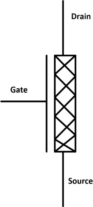
Figure 2:Symbol of the model in Cadence EDA tool
2.2 Optimization of the model using particle swarm optimization
A number of intelligent computing techniques,based on evolutionary computing and Swarm Intelligence(SI),are presented to solve various engineering applications.Particle Swarm Optimization(PSO)[Eberhart and Kennedy(1995)]have been proved to be efficient and is widely used.The major inspiration for all these methods stems from biological systems in nature.Some of the common characteristics of all these unconventional algorithms are that they are all population based,independent of derivatives and have employed probabilistic approach.These algorithms start with a set of solutions(called a parent population)instead of one trial solution,and generate a new set of trial solution by carrying out proper transitions,which is unique for each algorithm,in a stochastic manner.Using heuristic optimization techniques,best results can be obtained for the parameters available to model CNTFET.There are various optimization techniques available to optimize the devices in nano scale region.The high OFF-state leakage current due to band-to-band tunneling(BTBT)under high reverse gate voltages is still a major issue in CNTFETs.Many researchers have tried to suppress leakage current caused by BTBT by varying the doping profile and asymmetry between source/drain regions.
At this point, the little boy came out running towards his mother with tears in his eyes. He hugged her and felt an overwhelming5 sense of the sacrifice that his mother had made for him. He held her hand tightly6 for the rest of the day.
In this work,we propose PSO based optimization method to suppress the ambipolar conduction.The main objective of the optimization process is to extract an optimal value of the thickness and dielectric constant of the gate oxide to achieve suppression of ambipolar conduction without any loss in on-current.
The ithparticle(1≤i≤N,i∈Z)location is a viable solution in S and is represented asin particle swarm optimization.pbestrepresented as(pi1,… … pid,… ….piD)is the value of the ithparticle's best fitness i.e.,its best position.gbestrepresented asoris the best of pbest amongst all particles.The ithparticle's velocity is given as.With the acceleration constants c1and c2,the inertia weight,the ithparticle is handled by the Eq.(10)for every time step.UR()are some random values taken between 0 and 1.

where xid=xid+vid
The objective function is to maximize the Ion/Ioffratio which translates to suppression of ambipolar conduction.The parameters to be optimized are the gate oxide thickness and the dielectric constant.
In this work,the fitness function,f with M samples is taken as the ithparticle's drain current mean squared error and is given as in Eq.(11).

The calculated drain current based on the computation of PSO is the predicted value IDS,PSO.The targeted numerical function is given as IDS,Num.The PSO parameters are shown in Tab.1.
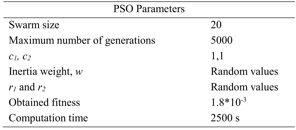
Table 1:PSO parameters
The steps of the PSO are shown in the flowchart in Fig.3.Tab.2 shows the optimized values of the thickness and gate dielectric constant for good Ion/Ioffratios.The thickness is found to be 50 nm and the dielectric constant is 25.Therefore,zirconium dioxide(ZrO2)whose dielctric constant is close to 25 is chosen.With the extracted optimized values from PSO,the SB CNTFET with 50 nm ZrO2dielectric was fabricated and is presented n the next section.

Figure 3:Flowchart of PSO
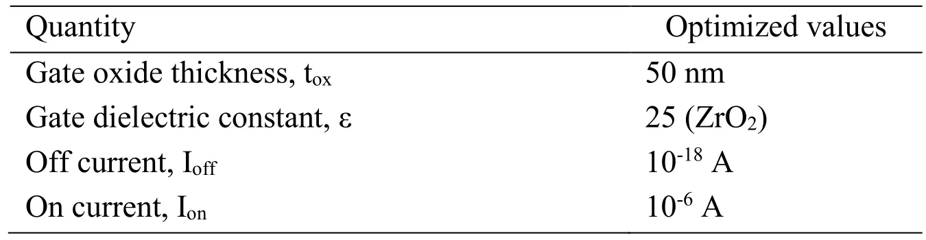
Table 2:Optimized parameters
3 Fabrication of SB CNTFET

Figure 4:Fabrication steps of the back gated SB CNTFET
The CNTs were spin coated over the dielectric layer to form a thin film of CNTs on both the devices.Deposition of CNTs by dispersing them in a solvent and spin coating is an excellent method to form a thin film of CNTs.The obvious advantages being the simplicity of the procedure,it's speed and to top it all it can be performed at room temperature.This process of dispersing CNTs and spin coating them,in due course,will enable large-scale fabrication of CNTFETs.The CNTs were bought in powdered form from Amorphous and Nanostructure Ltd.,USA.The SWCNTs are semiconducting and are 5-30 μm long with a purity of 95% CNTs and 90% SWCNTs.The outside diameter is measured as 1-2 nm and the inside diameter is 0.8-1.6 nm.The material characterization results showing that the SWCNTs are semiconducting can be found in http://www.nanoamor.com/inc/sdetail/9539.
For Spin coating,the CNTs were dispersed in a solvent Triton X 100.Triton X 100 gives better dispersion as well as good viscosity[Santagata,Baglieri and Tsantilis(2015)].It is 5% in aqueous solution.5mg of CNT was mixed with 1% of Triton X 100.The amount of Triton X required for 20 ml solution was calculated as follows:
Amount of Triton X 100(N0)in aqueous solution=5%.The required total percentage(N1)of Triton X 100 is 1%.Total volume of solution(V1)=20 ml.
Total volume of Triton X 100 required(V0)was calculated to be 4 ml using the relation in Eq.(12)

Therefore,4 ml of Triton X 100 was added with 16 ml of pure distilled water.5 mg of CNTs were added to this mixture and was dispersed by sonication.The dispersion was carried out using a tip sonicator.The time taken for proper dispersion of CNT was calculated using Eq.(13)

where E is the sonication energy which is 320J/ml and P is the output power of the sonicator[Kun and DaoHui(2013)]which is 80 W.V is the volume of the solution to be sonicated which is 20ml in this case.Therefore the time,t for sonication was calculated to be 80 minutes.Tip sonication gives a homogeneous solution with 0.229 poise viscosity which is favorable for spin coating.The SEM image of the dispersed CNT is shown in Fig.5.The dispersed CNTs were spin coated on to the dielectric surface of the silicon wafer of both the devices.A good coating ensures proper connectivity between electrodes.Both the spincoated devices were annealed at 150°C for ten minutes.The patterned metal electrodes were deposited over the CNT layer.Shadow masking or stencil lithography was used which gives patterns as imprints of the mask.Aluminium was deposited by thermal evaporation for the contact electrodes.

Figure 5:SEM image of the dispersed CNTs
4 Results and discussion
Ideally,the SB height can be tuned to any value just by selecting an appropriate metal with high work function for holes and low work function for electrons.Due to the Fermi level pinning at the metal interfaces,it is practically difficult to tune the SB height to zero.However,the Metal Induced Gap States does not establish Fermi level pinning for 1D channel materials[Javey,Guo,Wang et al.(2003)].This makes the metal contacted CNTFETs extremely desirable as the SB heights can be tuned by the work function of the metal contacts.
Guo et al.[Guo,Datta and Lundstrom(2004)]performed a numerical comparative study of the effect of thickness of oxides on the ambipolar behavior of CNTs.They have numerically proved that a thick dielectric suppresses the ambipolar behavior of CNTs.The same result is demonstrated experimentally.Fig.6 shows the comparison between the numerical simulation result by Guo et al.[Guo,Datta and Lundstrom(2004)]and our experimental result.The difference in the range of drain current is due to the small channel length in Guo et al.[Guo,Datta and Lundstrom(2004)](~15 nm).
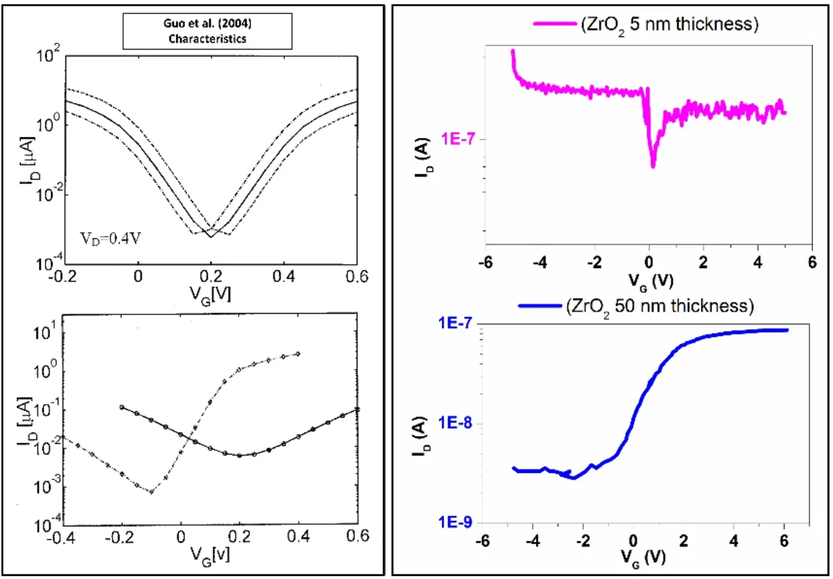
Figure 6:Comparison with the numerical simulation in Guo et al.[Guo,Datta and Lundstrom(2004)].Left plot shows the IV characteristics of the numerical simulation in Guo et al.[Guo,Datta and Lundstrom(2004)].Right plot is the IV characteristics for different gate oxide thickness(5 nm and 50 nm)of our experimental work
Aggressive scaling down of the gate oxide thickness makes the Schottky barriers very thin.This is because of the one-dimensional nature of CNTs[Odintsov(2000)].Therefore,when the gate dielectric is thin,the tunneling of electrons and holes occur since both SBs(source and drain side)become transparent resulting in ambipolar conduction.The length scale over which the bands bend at the source/drain metal contacts is defined by the gate oxide thickness.When the gate dielectric is thick,the SBs are not transparent for tunneling.The gate to source voltage alters the band such that tunneling of electrons or holes takes place.
The ID-VGcharacteristics of the ambipolar devices exhibit a V-shaped plot as shown in Fig.9.In devices with thick gate dielectric,the minimum of the V-shaped plot is shifted due to the trapped charges in the oxide.The suppression of ambipolar behavior can be observed.However,due to the increased thickness of the gate oxide layer,the on-current due to tunneling is reduced.A high-κ dielectric such as ZrO2with εk=22 is employed to increase the on-current due to thermionic emission.Thereby,the on-current is not affected.
Arijit Ray Chowdri[Chowdri(2007)]has demonstrated that on-current(Ion)can be improved by tube diameter modulation with thin high-κ dielectrics.It is proved that for smaller diameters(0.6 nm)of the nanotube the Ion/Ioffratio is better,but the on-current is poor.Nanotubes with a diameter of 2 nm resulted in higher on-current,but the Ion/Ioffratio is poor.The proposed work modulates the thickness of the barrier by increasing the thickness of the high-κ gate oxide to suppress ambipolar behavior without affecting the oncurrent.An experiment to measure IV characteristics of a device with a low-κ gate oxide such as SiO2with ε=3.9 and with thickness ~50 nm was conducted.The characteristics show a suppression of the ambipolar conduction,but the on-current was less(in the order of pico Amps)as shown in Fig.7(right).However,the measured characteristics for a device with high-κ gate oxide such as ZrO2with the same thickness(~50 nm)showed a higher on current while suppressing the ambipolar conduction.The current is in the order of micro amps as shown in Fig.7(left).The suppression is due to the thick gate oxide whereas the higher on-current is due to the high-κ gate oxide.Thus it is validated that the increased thickness of high-κ gate oxide suppresses the ambipolar behavior and gives good oncurrent.A comparative graph showing the decrease in on-current for a low-κ gate oxide and increase in on-current for a high-κ gate oxide is presented in Fig.7.

Figure 7:Comparison graph with different dielectrics.The plot in blue shows the characteristics for device with ZrO2(50 nm thickness)and plot in red shows the characteristics for device with SiO2(50 nm thickness)
The ID-VGcharacteristic for the device with thin gate oxide is shown in Fig.8.The SB CNTFET with thin gate oxide exhibited ambipolar behavior.The reason behind this is that the SB is thin and transparent to electrons and holes when the gate oxide is thin.
Fig.9[Pourfath(2007)]shows the actual behavior of thin SB CNTFETs where the conduction is ambipolar due to the increased band to band tunneling of holes as a result of the barrier lowering at the drain side for drain voltages greater than the gate voltage.The thickness of the barrier at the drain side is also reduced,thereby contributing tunneling current.This causes a damaging effect on the device operation in both the on and off state.In the proposed fabricated device with thick gate oxide,the barrier lowering and the reduction in barrier thickness at the drain side does not take place due to the thick gate oxide.Therefore by introducing an asymmetry,the ambipolar conduction is suppressed.

Figure 8:ID- VG Characteristics of the fabricated SB CNTFET with thin gate oxide(~5 nm)exhibiting ambipolar conduction
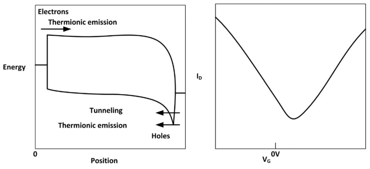
Figure 9:Band edge profile and output characteristics of an ambipolar CNTFET[Pourfath(2007)]
Fig.10 shows the ID-VGcharacteristics of the device with thick gate oxide,toxof 50 nm for VD=0.5 V and 1 V.This device did not exhibit ambipolar behavior.They exhibit unipolar characteristics when compared to the characteristics of the first device with the thin gate oxide.Thick SB is the reason for the suppression of the ambipolar conduction which is the result of thicker gate oxide.The SB limits the current at the metal-CNT contact.By changing the thickness of the tunneling barrier,the fringing field of the gate modulates the current.It is concluded that,in the second device,the conduction of electrons for negative gate voltages is suppressed due to the asymmetry introduced by the thick gate oxides.However,the on-current is compensated by the high-κ dielectric.
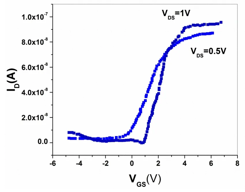
Figure 10:ID- VG characteristics of the device with thick gate oxide with suppressed ambipolar conduction
5 Conclusion
A mathematical model and an experimental demonstration of the suppression of the ambipolar property of CNTFETs are presented.The optimal gate oxide thickness and oxide dielectric constant were given by the particle swarm optimization.The ambipolar conduction is suppressed by employing thick high-κ gate oxides.The suppression is evident from the IDVGcharacteristics of both the devices.The use of thin high-κ dielectric improves the oncurrent like in a scaled down MOSFET.However,the ambipolar behavior was still observed.A thick high-κ dielectric ensured suppression of this behavior.The experimental results show that the device with thin gate oxide(~5 nm)exhibited ambipolar behavior,whereas the device with thick gate oxide(~50 nm)exhibited unipolar characteristics.The loss in on-current due to the thick gate oxide is compensated by the use of a high-κ dielectric ZrO2.The model was written in Verilog-A.Since the ambipolar conduction is suppressed,CNTFETs can be the next generation device for building robust digital circuits and reliable sensors and actuators for the IoT framework.
杂志排行

Computer Modeling In Engineering&Sciences的其它文章
- An Automated Approach to Generate Test Cases From Use Case Description Model
- Hybrid Deep VGG-NET Convolutional Classifier for Video Smoke Detection
- A Normal Contact Stiffness Model of Joint Surface Based on Fractal Theory
- Design of Smith Predictor Based Fractional Controller for Higher Order Time Delay Process
- Experimental Study and Finite Element Analysis on Ultimate Strength of Dual-Angle Cross Combined Section Under Compression
- IoT Based Approach in a Power System Network for Optimizing Distributed Generation Parameters