Superlubricity enabled dry transfer of non-encapsulated graphene∗
2019-02-25ZheYing应哲AolinDeng邓奥林BosaiLyu吕博赛LeleWang王乐乐TakashiTaniguchiKenjiWatanabeandZhiwenShi史志文
Zhe Ying(应哲),Aolin Deng(邓奥林),Bosai Lyu(吕博赛),Lele Wang(王乐乐),Takashi Taniguchi,Kenji Watanabe,and Zhiwen Shi(史志文),†
1 Key Laboratory of Artificial Structures and Quantum Control(Ministry of Education),School of Physics and Astronomy,Shanghai Jiao Tong University,Shanghai 200240,China
2 Collaborative Innovation Center of Advanced Microstructures,Nanjing 210093,China
3 National Institute for Materials Science,1-1 Namiki,Tsukuba 305-0044,Japan
Keywords:superlubricity,transfer,graphene,heterostructures
1.Introduction
As the family of atomically thin two-dimensional(2D)materials,including graphene,hexagonal boron nitride(hBN),transition metal dichalcogenides(TMDCs),etc.,is expanding,heterostructures composed of these materials provide an outstanding platform for exploring new phenomena and applications.[1-5]Currently,the most versatile technique for fabricating such heterostructures is direct mechanical assembly,in which a hexagonal boron nitride flake is typically employed to serve as a stamp to pick up other 2D materials,assemble them together,and finally lift them down onto the target substrate(the “pick-and-lift”method for short).[6-9]For heterostructures fabricated this way,the functional 2D crystal as the inner layer is typically encapsulated by hBN flakes.It is apparent that the completely assembled stack prohibits any direct contact with the inner layers.Therefore,such heterostructures are not quite appropriate for further investigation by surface characterization techniques,such as scanning tunneling microscope(STM),tip-enhanced Raman spectroscopy(TERS),and scanning near- field optical microscope(SNOM).In those circumstances,an exposed 2D flake without any coverage on desired substrates is required.In fact,methods for transferring bare 2D crystals without coverage are earlier and more mature.All these methods,however,require either a wet process at some stage[10,11]or a direct contact with polymer layers,[1,12]which will contaminate the 2D samples.In this article,we report an ultra-clean transfer method that allows the non-encapsulated graphene to be transferred onto a variety of substrates.Polymer contamination is completely avoided and no cleaning steps are required for further device fabrication or characterizations.Electrical and near- field optical measurements reveal the high quality of the transferred graphene samples.Our method is a large extension and improvement of the traditional“pick-and-lift”technique.
2.Method and demonstrations
Layered materials are characterized by weak inter-layer van der Waals force,which leads to many unusual operations,such as mechanical exfoliation of a 2D monolayer from 3D bulk crystals[13]and hetero-epitaxial growth of 2D materials.[14]More interestingly,it is recently reported that the graphene/hBN interface is super-lubricated where the sliding friction is orders of magnitude smaller than that measured for homogeneous graphite and other layered materials.[15-17]Such superlubricity has been exploited to achieve severalstriking effects,such as dynamically tunable heterostructures and thermal rotation.[18,19]For an hBN/graphene heterostructure on a substrate,if one pushes the top hBN flake with a tangential force,the hBN flake would probably slip upon the graphene layer and leave the graphene exposed at its original position.Based on such considerations,we develop a new all-dry transfer method,with which we are able to fabricate bare graphene on a variety of substrates.We first transfer hBN/graphene heterostructures onto a target substrate using standard “pick-and-lift”dry transfer method,[7]and then we use a stage-controlled micro-tip to push away the hBN layer,and finally acquire non-encapsulated graphene flakes on target substrates.Graphene transferred in this way is fully exposed without any coverage and ultra-clean without polymer contaminants.
Figure 1 illustrates the key step of removal of the toplayer hBN in the transfer process using a stage-controlled micro-probe.Similar to the standard dry transfer method,[7]we first use a polypropylene carbonate(PPC)membrane to pick up an hBN flake from an SiO2/Si substrate.We prefer to select relatively thick hBN flakes with thickness larger than 100 nm,because thick flakes will benefit our subsequent pushing steps.Next,we use this hBN flake to pick up a graphene flake.Then we release the hBN/graphene stack onto a target substrate by heating the PPC membrane up to∼95°C to reduce its viscidity and peeling it off.Finally,we use a microprobe(with radius∼1µm)to push and scrape slightly the top hBN flake from one of its edge.A probe station(ADVANCED PW-800)is employed to carry out the scraping process.In this step,we notice that the relatively thick hBN flake is more practicable.For a thin hBN flake,it is hard to apply a sufficient tangential force by the probe,unless we press the probe fiercely which may crack the whole stack and destroy the sample.After the scraping,the top hBN flake has a lateral displacement while the graphene stays at its original position due to larger static friction force between graphene and substrate.Since no polymer is in direct contact with graphene during the whole transfer process,the transferred graphene on target substrates is free of contaminants and no further cleaning steps are needed,such as annealing or cleaning by solvents.In the following,we will provide a few examples of transferring graphene flakes onto different substrates.
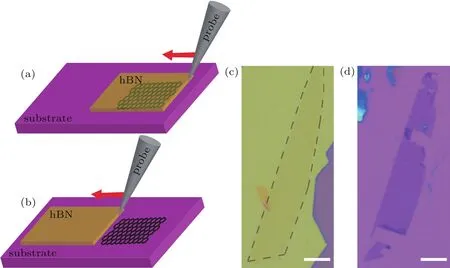
Fig.1.Schematic diagram of superlubricity enabled separation of graphene and hexagonal boron nitride(hBN)from an hBN/graphene stack.(a)An hBN/graphene stack on desired substrate.A probe with a radius of∼1µm is about to scrape and push away the top-layer hBN flake from its edge.(b)After the scraping,the hBN slips away and bare graphene is left.It is due to the superlubricity at the hBN/graphene interface,and the static friction between graphene and substrate is much larger than that of hBN/graphene interface.(c)and(d)Optical images of a typical sample before and after the removal of top-layer hBN flake.The dashed line in panel(c)denotes the outline of the graphene flake underneath hBN.The scale bar in panels(c)and(d)is 10µm.
To check the validity of the method,we first transfer a graphene flake from one SiO2/Si substrate to another SiO2/Si substrate,considering that graphene on SiO2/Si can be directly identified and located with an optical microscope.Figure 2(a)shows an exfoliated bilayer graphene flake on an SiO2/Si substrate.We use the standard “pick-and-lift”method to transfer this graphene flake onto another SiO2/Si substrate(Fig.2(b)).At this stage,the transferred graphene flake is covered by an hBN flake.After we scrape and push away the top hBN flake,bare graphene is left on the target SiO2/Si substrate(Fig.2(c)).Although part of the graphene flake is broken and missed,the successfully transferred part is very clean.The breakage of the transferred graphene comes from the uncertainty of the scrape process which is instrument limited.The cleanness of the transferred graphene is revealed by an atomic force microscope(AFM)image(Fig.2(d))of this graphene flake.To further examine whether there is any organic contamination on top of the graphene flake,we perform a nano-brooming process with an AFM tip on a 2µm×2µm area of the graphene(black dashed square region in Fig.2(d)).No accumulation of contaminants is found,which confirms the ultrahigh cleanness of the transferred graphene.
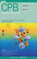
We further demonstrate transferring graphene onto transparent substrates,on which directly exfoliated monolayer graphene is typically difficult to identify or locate due to the extremely low optical contrast.For the transferred graphene fabricated with our method,there is typically a thick hBN flake nearby,which can serve as a natural mark to locate the transferred graphene flake and therefore is very useful in practice.Figures 3(a)and 3(b)are infrared scanning near- field optical microscope(IR-SNOM)and AFM topography images of transferred monolayer graphene on a quartz substrate,and figures 3(c)and 3(d)are IR-SNOM and AFM topography images of that on a mica substrate.A home-built IR-SNOM composed of a Bruker Innova AFM and a carbon dioxide laser with a wavelength of 10.6µm is used for the near- field IR imaging.Since mica is hydrophilic,graphene transferred with traditional wet process can easily get contaminated by solvents.[20]On the contrary,graphene samples transferred with our method are much cleaner with no contaminants and less water molecules,as shown in the topography images in Figs.3(b)and 3(d).

Fig.2.Demonstration of transferring a non-encapsulated graphene flake onto an SiO2/Si substrate.(a)A bilayer graphene flake on SiO2/Si substrate 1 fabricated using mechanical cleavage.(b)A transferred hBN/graphene stack on SiO2/Si substrate 2 using standard “pick-and-lift”method.(c)After probe-scraping and removal of the top-layer hBN,bare graphene flake is left on substrate 2.(d)AFM topography image of transferred graphene.Although the transferred graphene is damaged after we scrape away the top hBN flake,which can be attributed to our instrument limitation,the remaining graphene region is very clean.The dashed square region(2µm×2µm)is nano-broomed by AFM tip and no accumulation of contaminations is observed,which confirms the ultra-cleanness of the transferred graphene sample.The scale bar in panels(a)-(c)is 20µm,and in panel(d)is 5µm.
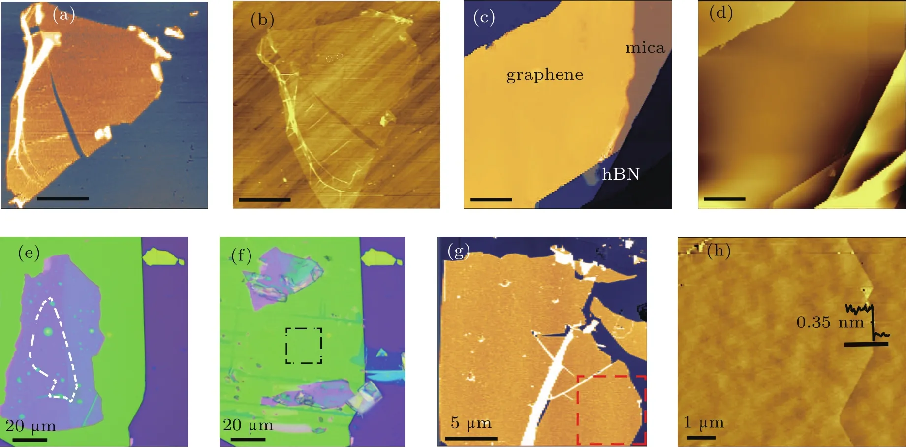
Fig.3.Examples of transferring non-encapsulated graphene onto quartz,mica,and hBN substrates.(a)and(b)Near- field infrared and AFM topography imagesoftransferred monolayergraphene on quartz substrate.(c)and(d)Near- field infrared and AFMtopography imagesoftransferred graphene on mica substrate.The scale bar in panels(a)-(d)is 2µm.(e)Optical image of hBN/graphene/hBN stack on SiO2/Si substrate and panel(f)that after the removal of the top hBN flake.Monolayer graphene on thick hBN substrate is invisible in the optical image and we do nearfield infrared characterization for dashed square region in panel(f).(g)The near- field infrared image of transferred graphene on hBN.The bright region represents graphene and the dark region represents hBN.(h)AFM topography image of dashed square region in panel(g).The transferred graphene on hBN is ultra-clean.
Next,we demonstrate transferring bare graphene onto an hBN substrate.Graphene on top of hBN crystals is a remarkable heterostructure.Due to the atomically flatness of hBN and the 1.8%lattice mismatch between the two types of crystals,many interesting physical phenomena,such as emergent Dirac cone,[14,21]Hofstadter’s butter fly,[2-4]and mixing of pseudospin,[22]have been observed in graphene/hBN heterostructures.To obtain a graphene/hBN heterostructure,we first fabricate an hBN encapsulated graphene stack(hBN/graphene/hBN)using “pick-and-lift”technique,as shown in Fig.3(e).Then we scrape and push away the top hBN flake,as displayed in Fig.3(f).One could not identify the monolayer graphene from the optical micrograph displayed in Fig.3(f)due to the extremely low optical contrast.However,the graphene flake clearly shows up in the IR-SNOM image(Fig.3(g)),because graphene has much stronger IR response than hBN substrate due to its high optical conductivity.A zoom-in topographic image of the lower right corner region(Fig.3(h))again shows the cleanness of the graphene flake transferred with all-dry mechanical processes.
3.Near- field optical and transport characterization
To further examine the high quality of the transferred graphene samples,we perform near- field optical measurement on a transferred bilayer graphene on an hBN substrate,by which plasmonic response of the charge carrier in the sample can be probed.[23-26]A carbon dioxide laser beam with wavelength of 10.6µm is focused on a metallized AFM tip to excite plasmons in graphene.In order to observe plasmons,the transferred graphene is connected by an electrode,with which we are able to tune the carrier density of the sample by applying a voltage between the graphene and the silicon layer of the substrate.Figure 4(a)shows the topography(left panel)of the bilayer graphene with a height of∼0.8 nm and the corresponding plasmonic interference pattern(right panel)at a gate voltage of 28 V.A line profile of plasmons is shown in Fig.4(b),in which up to seven interference fringes can be observed near graphene edge,indicating the low electronic loss and high quality of the transferred graphene sample.[23,27]

Fig.4.Device fabrication,and electrical and near- field optical characterization of the transferred graphene samples.(a)AFM topography(left panel)and near- field infrared(right panel)images of a bare graphene flake on hBN substrate.(b)Line profile of plasmon interference pattern taken along the line-cut in panel(a).The scale bar in panel(a)is 200 nm.(c)Illustration of the process for fabricating an hBN encapsulated graphene device.Part of the top hBN flake is scraped away,so that part of graphene region is exposed which can be used for connecting electrodes.(d)Resistivity of the device as a function of gate voltage at liquid nitrogen temperature,from which a carrier mobility of∼ 11000 cm2·V-1·s-1 is extracted.Inset shows the corresponding conductivity near the charge neutral point and optical micrograph of the device.
The superlubricity enabled removal of top-layer hBN also provides a new approach to fabricate electrodes onto hBN-encapsulated graphene samples.For encapsulated graphene samples,usually electrical measurement is only realizable with edge-contact configuration which requires E-beam lithography followed by plasma etching process.[7]Here,we show that using a stage-controlled probe to scrape the top hBN flake can result in uncovered graphene regions,which can be used to connect electrodes on graphene.The schematic of the fabricating process is displayed in Fig.4(c).Metal film electrodes composed of 2-nm Ti and 80-nm Au are fabricated using an E-beam evaporator(Sky technology development,DZS-500)associated with a shadow mask.Transport measurement is performed in a liquid nitrogen Dewar.Keithley 2400 sourcemeters are used to supply both gate voltage and source-drain voltage,and to measure the source-drain current.Figure 4(d)shows the electrical transport data of a monolayer graphene device fabricated this way measured at liquid nitrogen temperature.[13]The inset of Fig.4(d)presents the corresponding conductivity curve near the charge neutral point and optical micrograph of the device.The carrier mobilityµcan be extracted by the formula,µ =(1/C)dσ/d Vg,where C is the capacitance of the gate.[1]The extracted carrier mobility µ is∼ 11000 cm2·V-1·s-1,which is comparable to that of graphene on hBNsubstrate reported in the previous studies[1,9]and is much higher than that of graphene on SiO2/Si substrate.It is noted that there is a bump on the hole side in the transport characteristic curve in Fig.4(d),which probably comes from the Moiré superlattice and the corresponding superlattice Dirac point induced by the unintentional alignment.[14,21]The obtained high carrier mobility and the observation of superlattice Dirac point imply the high quality of our device and the success of the fabrication method.In addition to the edgecontact method,we develop a new and simpler approach to make electrodes onto the sandwiched high quality graphene samples.
4.Conclusion and perspectives
In conclusion,we develop an all-dry mechanical transfer method for transferring ultra-clean and non-encapsulated graphene samples by employing the superlubricity in graphene/hBN interface.We demonstrate transferring nonencapsulated graphene flakes onto a variety of substrates.The transferred bare graphene samples are free ofpolymerresidues and of high quality,which is confirmed by clean AFM topography,high electron mobility,and weak plasmons loss.Moreover,the superlubricity enabled removal of top-layer hBN provides a new and simpler approach to fabricate electrodes onto hBN-encapsulated graphene samples.The method developed here should be applicable to a wide range of 2D materials that can form superlubricated interfaceswith hBNcrystals,and can be further improved by using a precision machinery and automated robotic stacking of 2D materials.[28]
Acknowledgement
Zhi-Wen Shi acknowledges support from the Thousand Youth Talents Plan and the Program for Professor of Special Appointment(Eastern Scholar)at Shanghai Institutions of Higher Learning.Kenji Watanabe and Takashi Taniguchi acknowledge support from the Elemental Strategy Initiative conducted by the MEXT,Japan and the CREST(JPMJCR15F3),JST.
猜你喜欢
杂志排行
Chinese Physics B的其它文章
- Physics of quantum coherence in spin systems∗
- Recent progress of infrared photodetectors based on lead chalcogenide colloidal quantum dots∗
- Progress in quantum well and quantum cascade infrared photodetectors in SITP∗
- Recent advances in Ga-based solar-blind photodetectors∗
- Development of long-wavelength infrared detector and its space-based application requirements∗
- Transition of photoconductive and photovoltaic operation modes in amorphous Ga2O3-based solar-blind detectors tuned by oxygen vacancies∗