脉冲激光沉积制备非晶La0.75Sr 0.25MnO3薄膜用于半透明阻变存储器
2018-04-10张佳旗吴小峰马新育黄科科冯守华
张佳旗 吴小峰 马新育 袁 龙 黄科科 冯守华
0 Introduction
Resistive random access memory (RRAM)receives considerable research interests recently due to their fast switching,good non-volatily,low power consumption and etc.It has also been considered as an appropriate candidate for simulating artificial synapse[1-3].The RRAM devices express an current/voltage input history dependent resistance,which records the resistance by electric field induced active ions migration and accumulation that causes local conductive filament of the device[4].The critical component of RRAM devices is the interlayer accomodating ionic transfer channel to form metallic filament by electrochemical metallization[5]. Thus,materials with low electronic conductivity and high ionic conductivy are typically expected to be proper RRAM intermediate layer candidates[6].
Various materials have been employed as the interlayers in RRAM,such as elementary substance[7-8],binary metal oxides[5,9],nitrides[10],polymers[11-12]and perovskitestructureoxides[13-14].Amongthem,perovskite manganite oxides with mixed-valence states of Mn have attracted great attention due to the potential to integrate resistive switching and colossal magnetoresistance(CMR)properties[15]into one system[13,16].The CMR effect of perovskite magnatites results from the intrinsic magnetic exchange behavior between the charge ordered arrangement of Mn3+and Mn4+in the long range octahedral MnO6corner-shared structures[17-18]. Recently,amorphous La1-xSrxMnO3thin films,deposited by radio frequency (RF)magnetron sputtering,have been applied to the non-volatile bipolar resistive switching devices with high-frequency dependent pinched hysteresis loops[13-14,19].
Pulsed laser deposition(PLD)is another deposition approach for the perovskite magnatite films,which is a versatile physical vapor deposition for fabricating multi-component oxide films with precisely controlled stoichiometry[20].In previous work,our group have successfully fabricated high quality perovskite structure manganites and ferrites films by PLD for the application of optoelectronics and photoelectrocatalysts[21-22].Here we explore the PLD fabricated amorphous La0.75Sr0.25MnO3(a-LSMO)layers as intermediate layers in RRAM cells.
The intermediate layers of RRAM are characterized by different approaches.The characterization of the conduction channel in the interlayer,however,is a key study because the conduction channel is one important resistive switching mechanism for the RRAM.Different methods have been utilized to detect the conduction channels.For example,conductive atomic force microscopy(c-AFM)can provide current mapping images under different reading bias[14].Temperature dependence of the resistances of ON and OFF states reflects different electronic transport behaviors of metals and semiconductors,respectively.Top-view images by scanning electron microscope(SEM)reveal the conductive filament growth[23].In this work,cross-sectional image of interelectrode region of our RRAM cell is directly observed by the highresolution transmission electron microscope(HRTEM),which clearly shows the Ag filament formation at the interface between Ag and the a-LSMO layers.In addition to the electrochemically active Ag top electrode,electrochemically inert indium tin oxide(ITO)is used as bottom electrode for the purpose of fabricating low-cost and transparent memristor.Between two electrodes,10-nm-thick a-LSMO is deposited by pulsed laser deposition (PLD)as the interlayer with high transparency.
In this paper, we successfully fabricate amorphous LSMO ultrathin layer by pulsed layer deposition and fabricate RRAM device in a structure of ITO/a-LSMO/Ag.The memory cells show nonvolatile bipolar resistance switching behavior with good durability and reproducebility.To the best of our knowledge,we are the first to report RRAM device based on PLD prepared a-LSMO.The resistive switching mechanism of our devices is investigated by cross-sectional view of HRTEM analysis,which proves that the memristive behavior is governed by the growth and dissolution of metallic filament of Ag nanoparticles in amorphous LSMO layer.
1 Experimental
1.1 Device fabrication
The tin doped indium oxide (ITO)coated glass substrates and La0.75Sr0.25MnO3(LSMO)target were both purchased from KJMTI Co.,Ltd,China.The ITO substrates with the size of 1.5 cm×1.5 cm were processed by ultrasonic cleaning in sequence of acetone,ethanol and deionized water,and finally dried in compressed N2flow.Then the substrates were mounted on a metal heater plate by silver paint and transferred into the chamber.The chamber base pressure was 1.1×10⁻³Pa.A excimer laser(KrF,248 nm)with repetition rate of 5 Hz and energy fluence of 1.5 J·cm-2ablated the LSMO target and the plume deposited perpendicularly to the substrate.The targetsubstrate distance was 65 mm.The depositions were carried out in the flowing oxygen of 13.3 Pa with the substrate temperature fixed at 573 K.Finally,the asdeposited films were cooled down to room temperature with the rate of 10 K·min-1.Circular Ag top electrodes with the thickness of 100 nm and the diameter of 300μm were deposited on the resultant films by thermal evaporation under vacuum through a stainless steel mask.
1.2 Characterization
The crystalline properties were evaluated by X-ray diffraction(XRD,Rigaku D/Max2550)with Cu Kα radiation(λ=0.154 18 nm)from 10°to 90°at a step width of 0.02°with working voltage of 40 kV and working current of 30 mA.The ultrathin lamellar fabrication and microstructure for the cross-sectional characterization were carried out on electron/focused ion dual beam system (FIB,FEI Helios 600i)using ion beam accelerating voltages of 30,5 and 2 kV sequentially and transmission electron microcope(TEM,FEI Tecnai F20)at 200 kV,respectively.Optical properties of the films were characterized by a UV/VIS/NIR spectrometer(Shimadzu UV-2450)with ambient air as the reference signal.
1.3 Device performance measurement
The electrical characteristics of the ITO/a-LSMO/Ag RRAM cells were analyzed at room temperature in air.A bias voltage was applied to the top electrode while the ITObottom electrode was grounded.
2 Results and discussion
2.1 Material structure analysis
The structure of the RRAM devices was characterized by X-ray diffraction,shown in Fig.1.The diffraction peaks of ITO substrate can be indexed with high crystallinity (PDF No.39-1058).No peaks are detected for LSMO films,which may result from the ultra-thin 10-nm-thick layer or its intrinsic amorphous nature.More structaral analysis of LSMO films proves that the LSMO films are amorphous,shown in the undermentioned TEM results.For Ag electrodes,characteristic peaks of Ag layer that deposited on the surface of a-LSMO are detected in accordance with PDF No.41-1402.These results indicate that a RRAM device with a sandwiched structure of Ag/a-LSMO/ITO has been fabricated.
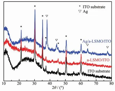
Fig.1 X-ray diffraction patterns of ITOsubstrate,amorphous LSMOfilms on ITOsubstrate and the Ag/a-LSMO/ITOstack
2.2 Transmittance spectroscopy
The bandgap of LSMO is only 1.0 eV in its bulk form,which results in low transparency in visible region[24].However,when the thickness of LSMO film is reduced to~10 nm,the transparency can be significantly increased.Transmittance spectra of ITO substrate and a-LSMO/ITO stack are shown in Fig.2.The bare ITO glass substrate under the same annealing condition as the a-LSMOfabrication process shows high transmission (above 80%)in the wavel-ength over 350~900 nm,which covers the whole visible region.And the a-LSMO/ITO stack keeps high transmittance with slight absorption at ca.400 nm,which is consistent with the reference[25].Therefore,we demonstrate a semi-transparent device fabricated by this method.
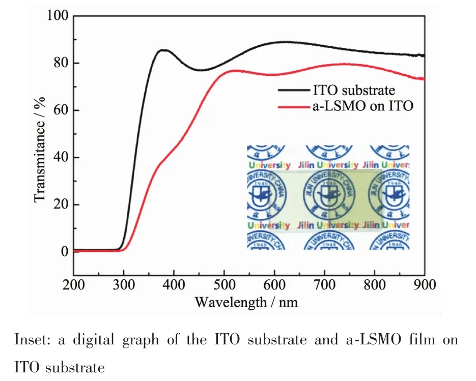
Fig.2 Transmittance spectra of ITOsubstrate and a-LSMO film on ITO
2.3 Resistive switching properties
Fig.3 shows the repeatable memeristive switching behavior of the ITO/a-LSMO/Ag device.Schematic configuration of our Ag/a-LSMO/ITO device structure is depicted in the inset of Fig.3a.The LSMO intelayer was deposited on ITO substrate by PLD with low kinetic energy as an insulating layer.Relatively low deposition temperature prevents the crystallization process because the incident particles has insufficient energy to move towards the surface to the sites where crystallization happens.Ag electrode with thickness of 100 nm and diameter of 300μm was deposited by thermal evaporation.The device clearly shows the resistive switching behavior in the bias voltage range from-2.0 to 1.5 V (Fig.3a).The memory window and onset voltage show negligible change in the measurement over 40 repeated cycles (Fig.3b).The resistances of ON and OFF states in 43 I-V cycles were collected under a small reading voltage of 0.1 V.Both resistance variations of high and low resistance states during cycles are small,which keeps the memory window a high value of ROFF/RONover 20 without degradation.The set and reset voltages of the device also show narrow distribution in the sequential cycling loops,which demonstrates stable ON and OFF responses.Here,the reset voltages are obtained under compliance current conditions.The average voltages for SET and RESET processes are 0.66 and-1.60 V,respectively (Fig.3c).These results reveal the stable endurance performance of the memristive properties of our Ag/a-LSMO/ITO RRAM device.Resistance retention of each state of the device is illustrated in Fig.3d.The ratio of ROFF/RONis over one order of degree with clear retention time of 103s,which keeps nearly constant and confirms the non-volatile characteristic of our device.

Fig.3 Resistive switching behavior of Ag/a-LSMO/ITO device:(a)Current-voltage hysteresis showing the cycling performance of the device;(b)Resistances of the device measured over 40 cycles;(c)Threshold voltages of the Ag/a-LSMO/ITO device over 40 cycles;(d)Retention performance of the Ag/a-LSMO/ITO device under a small reading voltage of 0.1 V at room temperature
2.4 Resistance switching mechanism
In order to investigate the resistance switching mechanism of the as-fabricated Ag/a-LSMO/ITO device,the I-V curves are plotted in a double logarithmic scale (Fig.4).Linear lines with a slope of~1 are found both in high and low resistive states,which indicates Ohmic transport of the current from Ag and ITO electrodes[26].A nonlinear relationship of the lg I-lg V is found in the high voltage region with a slope of 2.11,which may result from the space charge limited current(SCLC)according to the Child′s Law with the exponential relation of I-V2[26].Thus,when the device transforms from On state to OFF state,its conductive behavior experiences a change from Ohmic conducting to charge hopping by the break of the metallic filament.
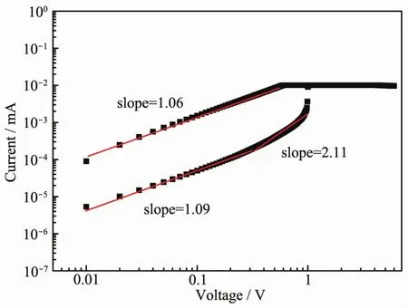
Fig.4 Conducting behaviour of Ag/a-LSMO/ITO device in double logarithmic plot
Resistance switching property of the device is based on the electrochemical metal deposition and dissolution processes.Fig.5 shows the electrochemical metallization mechanism of our RRAM cells with I-V hysteresis curves by applying quasi-static triangular bias-voltage signal.The top electrode of our device is Ag,an electrochemically active metal,with ITO as electrochemically inert counter electrode.Amorphous LSMO thin film layer was deposited as a solid electrolyte for Ag+conductor,which was sandwiched between Ag and ITO.In the initial state(OFF),no Ag species can be deposited on ITO electrode,and correspondingly the device shows a high resistance state (Fig.5d).When a sufficiently high positive bias is applied between Ag and ITO electrodes,Ag+ions dissociate from the Ag electrode,then migrate to the ITO side and finally form Ag nanoparticles on the interface between a-LSMO and ITO (Fig.5a).High electric field(2.5×10⁷V·m-1)facilitates the migration of Ag+ions across non-conductive a-LSMO electrolyte.Anodic oxidation(Ag→Ag++e-)and cathodic reduction(Ag++e-→Ag)reactions occur on Ag and ITO electrodes,respectively.Metallic filament forms in the electric assistant deposition of Ag+,which grows preferntially in the direction of the electric field.After the filament reaches the Ag electrode,the device switches to ON state with low resistance (Fig.5b).The amount of Ag nanoclusters determines the resistance of the device,which results from the charge transfer from Ag to ITO.The Ag+migration between two electrodes is affected by the dissolution rate of Ag+from anode and deposition rate of Ag nanoparticle from the reduced Ag+on cathode with positive bias.Thus,the switching behavior of the device depends on the kinetics of the two processes.The device remains ON state until a suffciently large opposite voltage applied that dissolves the filament between two electrodes and changes the device to OFF state (Fig.5c).OFF state will continue with disconnected metallic filament until another pulse of positive voltage applied,which propels to a next cycle of the device.

Fig.5 Representative current-voltage curve of Ag/a-LSMO/ITO device using a triangular voltage sweep with bipolar switching characteristics:(a)Set of the memristor;(b)Formation of conductive filament;(c)RESET;(d)OFF state
To further understand the dynamic growth process of the metallic filament formation of Ag nanoparticles from OFF state to ON state,we have used high-resolution transmisson electron microscopy(HRTEM)to detect the cross-section of the device,shown in Fig.6.Clear interfaces of ITO/LSMO and LSMO/Ag are detected in the as-prepared device(Fig.6a).Zoom-in view shows an uniform and smooth LSMO layer with high contrast against the neighbour layers of ITO and Ag (Fig.6b).The ultra-thin 10-nmthick LSMO layer shows good contact with the ITO substrate,which originates from the high kinetic energy of the incident particle from pulsed laser depostion technique.Obvious crystal lattices could be discriminated from the areas of ITO and Ag in Fig.6c,which reveals the crystalline nature of ITO and Ag films.While LSMO layer,deposited at 300℃,shows amorphous characteristic without any measurable lattice fringes.It should be emphasised that the deposition temperature of 300℃is carefully selected to make amorphous films with smooth and compact morphology.Lower deposition temperature leads to noncompact films (not shown here)and higher temperature may cause the crystallization of LSMO[27-28].The amorphous dielectric layer does not only increase the resistance at OFF state,but may also provide sufficient channels for Ag+migration due to numerous granular boundaries.
Fig.6a~c depict the as-fabricated device on OFF state,while Fig.6d shows the device on ON state.It can be seen that the a-LSMO layer becomes thinner in some positions of the interfaces,where the pristine 10-nm a-LSMO is reduced to 2 nm,accompanied by the insertion of Ag into the LSMO layer.This result corroborates the formation of Ag filament on ON state.
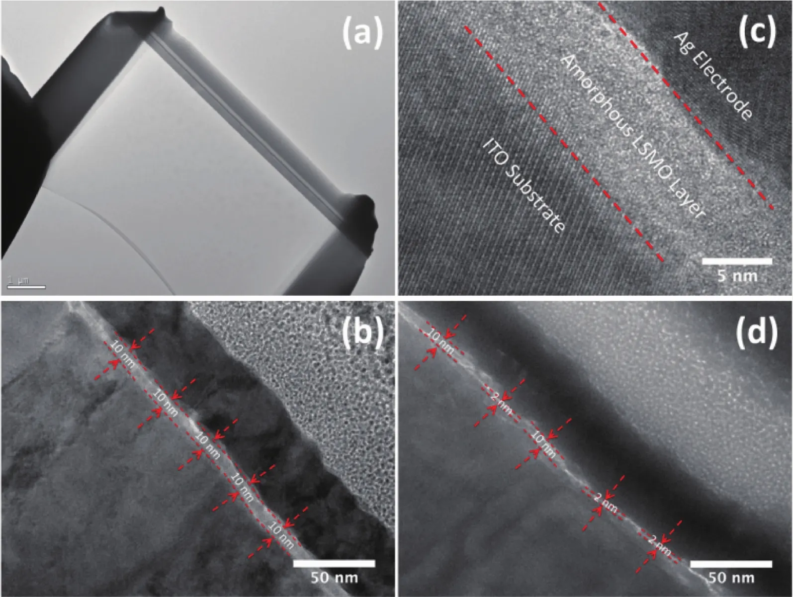
Fig.6 Morphological and structural analysis of the Ag/a-LSMO/ITO device by HRTEM:(a)Cross-section image of the slice of Ag/a-LSMO/ITO device fabricated by FIB;(b)Uniform 10-nm-thick amorphous LSMO layer sandwiched between the Ag and ITOlayers in OFF state;(c)Enlarged graph showing obvious lattice fringes of crystalline ITO and Ag and no detection of fringes in amorphous LSMO layer;(d)Formation of silver filament with the thinning of the a-LSMO layer in ON state
3 Conclusions
In summary,we have successfully fabricated a memristive switching device of Ag/a-LSMO/ITO with good non-volatile and bipolar resistance switching behavior.Ultra-thin amorphous LSMO interlayer fabricated by the pulsed laser deposition technique is proven compact and smooth,which promotes the RRAM device performance.This device shows large ON/OFF state switching resistance ratio and reproducible writing/erasing endurance with high retention times.Bottom ITO substrate and ultra-thin a-LSMO layer also allow semi-transparent device fabrication.The resistance switching behavior is attributed to the growth and break of Ag metallic filament in a-LSMO layer according to the electrochemical metallization theory.The fabricated Ag/a-LSMO/ITO device shows great potential for multibit data storage modes,which could be a promising candidate for non-volatile RRAM applications.
Acknowledgements:This work was supported by the National Natural Science Foundation of China (Grants No.21427802,21671076).
[1]Jo SH,Chang T,Ebong I,et al.Nano Lett.,2010,10:1297-1301
[2]Wang Z Q,Xu H Y,Li X H,et al.Adv.Funct.Mater.,2012,22:2759-2765
[3]Kim H,Sah M P,Yang C,et al.Proc.IEEE,2012,100:2061-2070
[4]Waser R,Dittmann R,Staikov C,et al.Adv.Mater.,2009,21:2632-2663
[5]Yang JJ,Strukov DB,Stewart DR.Nat.Nanotechnol.,2012,8:13-24
[6]Waser R,Aono M.Nat.Mater.,2007,6:833-840
[7]Jo SH,Kim K H,Lu W.Nano Lett.,2009,9:870-874
[8]Chai Y,Wu Y,Takei K,et al.IEEETrans.Electron Devices,2011,58:3933-3939
[9]Choi B J,Torrezan A C,Norris K J,et al.Nano Lett.,2013,13:3213-3217
[10]Kim H D,An H M,Lee E B,et al.IEEE Trans.Electron Devices,2011,58:3566-3573
[11]Chu C W,Ouyang J,Tseng J H,et al.Adv.Mater.,2005,17:1440-1443
[12]Kang N G,Cho B,Kang B G,et al.Adv.Mater.,2012,24:385-390
[13]Liu D,Wang N,Wang G,et al.Appl.Phys.Lett.,2013,102:134105
[14]Liu D,Cheng H,Zhu X,et al.ACSAppl.Mater.Interfaces,2013,5:11258-11264
[15]Tokura Y,Tomioka Y.J.Magn.Magn.Mater.,1999,200:1-23
[16]Liu S Q,Wu N J,Ignatiev A.Appl.Phys.Lett.,2000,76:2749-2751
[17]Moritomo Y,Kuwahara H,Tomioka Y,et al.Phys.Rev.B,1997,55:7549-7556
[18]Renner C,Aeppli G,Kim B G,et al.Nature,2002,416:518-521
[19]Liu D Q,Cheng H F,Wang G,et al.IEEE Electron Device Lett.,2013,34:1506-1508
[20]O′Sullivan M,Hadermann J,Dyer M S,et al.Nat.Chem.,2016,8:347-353
[21]Zhang J Q,Huang K K,Si W Z,et al.Sci.China,Ser.B Chem.,2013,56:583-587
[22]Sun Y,Wu X,Yuan L,et al.Chem.Commun.,2017,53:2499-2502
[23]Sun H,Liu Q,Li C,et al.Adv.Funct.Mater.,2014,24:5679-5686
[24]Qiu J,Lu H B,Jin K J,et al.Phys.B:Condens.Matter,2007,400:66-69
[25]Turky A O,Rashad M M,Hassan A M,et al.RSC Adv.,2016,6:17980-17986
[26]Zhang JJ,Sun H J,Li Y,et al.Appl.Phys.Lett.,2013,102:183513
[27]Pailloux F,Lyonnet R,Maurice J L,et al.Appl.Surf.Sci.,2001,177:263-267
[28]Walter T,Dorr K,Muller K H,et al.Appl.Phys.Lett.,1999,74:2218-2220