PCB阻抗测试模块设计研究
2017-10-21蓝春华张鸿伟张柏勇
蓝春华 张鸿伟 张柏勇
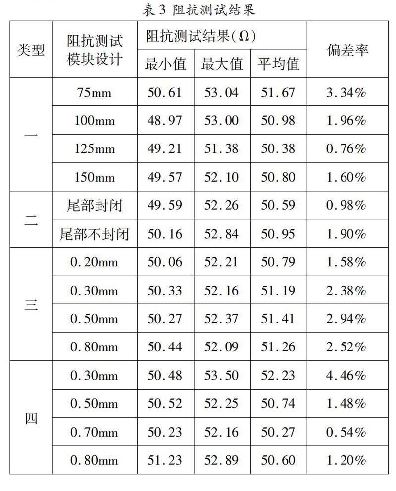

摘要:信号高频、高速化发展对PCB阻抗精度要求越来越高。常用PCB阻抗测试模块设计方法缺乏阻抗测试模块的精细化设计,因此测试模块中的测量值不能高精度体现出PCB实际的阻抗值。文章从阻抗线长度、阻抗线尾部状态、阻抗测试孔隔离环宽、阻抗线与周边铺铜间距共四个因素设计不同的阻抗测试模块,研究与实验PCB阻抗测试模块的最佳设计。
关键词:阻抗测试模块;阻抗线;阻抗值
Abstract:Signals high frequency, high speed development of PCB impedance accuracy requirements are getting higher and higher.The commonly used PCB impedance test module design method lacks the fine design of the impedance testing module, so the measured values in the test module can not reflect the actual impedance value of PCB.In this article shows four different factors design of impedance test module :the impedance line length, line tail status, test hole isolation ring width, line and the surrounding copper spacing, study and do Experiments to choice the best disgn for PCB impedance test module.
Key words:Impedance test module; impedance line; impedance value
信號高频、高速化发展对信号的完整性要求越来越严格,对PCB阻抗精度提出更高的要求。承载PCB主要信号传递的是阻抗线部分。基于PCB有效单元内的阻抗线难以单独测量,在PCB工作拼版有效单元中设计相同条件的阻抗测试模块,在PCB蚀刻后和阻焊后对阻抗测试模块测量。传统PCB阻抗测试模块设计在PCB工作拼版的中间位置,为改善阻抗线和阻抗线周边位置的镀铜均匀性,通常在阻抗线边缘设计铺铜,对测试模块中的阻抗线长短、测试孔隔离环宽、铺铜与阻抗线的间距等工程设计方面,缺乏精细阻抗测试模块设计,因此测试模块中的测量值不能高精度体现出PCB实际的阻抗值。本文从阻抗线长度、阻抗线尾部状态、阻抗测试孔隔离环宽、阻抗线与周边铺铜间距共四个因素设计不同的阻抗测试模块,研究与实验PCB阻抗测试模块最佳设计,为阻抗PCB工程设计优化提供依据。
1 实验
1.1 实验工程设计
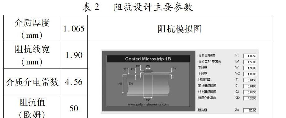
从阻抗线长度、阻抗线尾部状态、阻抗测试孔隔离环宽 、阻抗线与周边铺铜间距共四个方面的影响因素,设计不同规格的阻抗测试模块,具体如表1所述。……
