Design and establishment of a multi-function stop watch
2016-11-12ZhaoRuimin
Zhao Ruimin
(University of Liverpool,Liverpool L69 3BX,the Great Britain)
Design and establishment of a multi-function stop watch
Zhao Ruimin
(University of Liverpool,Liverpool L69 3BX,the Great Britain)
This report intends to record the conduction process of the stopwatch project.The project requirement was to build a digital clock circuit that can counter 1 minute on a breadboard using at least two counters.The achievement of this project of the group was that a digital clock that included three counters with additional functions such as buzzer,speeding shifting,and preset functions was constructed and simulated successfully.the apparatus used were primarily IC chips such as 74160,7447 and a big breadboard to build complex and big circuit that was designed.An expected future improvement of conducting this kind of project was that the circuit out-looking was expected to be more clear and beautiful if possible.To achieve this,skillful wiring ability and enough wiring practice are needed.
stop watch;555 timer;logic gate;IC;Multisim;PSPICE
0 Introduction
This project was to design and simulate a circuit for a digital clock that counts from 1 to 59 seconds with switches to control the circuit by pausing,resetting or turning on/ off it.The clock should be built on a breadboard using electronic components including IC chips - 74160[1],7447,7404,7408[2]etc,7-segment LED[3],switches,buzzer and other logic gates.The accuracy degree of counters is set to 0.1 by adding one more counters(74160).The buzzer rings every half minute(when reaching 29/59 seconds).The LEDs bright each time when the 1 second unit bit changes digit.
The whole complete simulation circuit screenshot is presented in Figure 1.
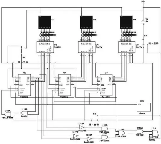
Figure 1 Whole Circuit
As can be seen in Figure 2,the circuit primarily consists of these modules:timer,three counters,three decoders and their connected 7-segment LED,a buzzer and its connected logic gates,and three switches of pausing/ turn-on(off)/reset.
A brief summary of how this circuit work can be like this:first,the timer provides a clock signal which is actually a rectangular waveform signal;then,since the counters in this circuit are designed to be synchronous counters,this clock signal is transported into the “CLK”pins of each counter(from left to right are respectively 10,1,and 0.1 bit);subsequently,the counters output their correspondingly generated signals from “QA,QB,QC,and QD” pins into their connected decoders so as to drive the LED bright as expected to display the digits.
Simultaneously,the buzzer rings every half minutes thanks to the decoder system connected with it which ensures that the input signal of buzzer is 1 only when the output of 10-bit counter is 2 or 5 and the output of 1-bit counter is 9;and an extra LED light is connected between the “RCO” pin of the 0.1 bit counter and the ground so that it can only bright when the “RCO” is high which means that the digit of the 0.1-bit counter is changing from 9 to 0.
1 Method and Result
1.1 Timer System
This circuit based on 555 timer IC[4-5]is in the mode which produces “never stable” output in the form of a rectangular waveform clock signal.It primarily consists of a 555 timer IC chip,two resistors,and two capacitors.
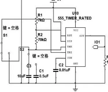
Figure 2 Timer
The input voltages of these two pins are the same and totaled depend on the voltage across the capacitor “C1”.The other two inputs of the comparators as pair of those two outside inputs respectively are decided by the voltage level of VCC the upper one in pair of “THRES” is and the lower one in pair of “TRIG” is due to the voltage division principle along the vertical line starting from VCC and end at GND through two identical inner resistors.
The clear signal relation of all these comparator inputs and outputs,Latch output,and transistor base voltage are listed in Table 1 as shown.

Table 1 Signal Relation
According to a series of calculations based on the 555 timer configuration,we first chose C1 to be 1µF due to its rich availability in lab,and the frequency f was set to be 0.1 since the least bit is 0.1 bit.Then we calculated the corresponding proper resistances of resistors which are R1 = 7 kΩ and R2 = 70 kΩ.
The simulation waveform graph in one second(that is ten periods in this case)is presented below in Figure 3 where the red wave is the voltage of capacitor and the green one is that of the timer output signal.
1.2 Counter System
The counter system consists of three counters,that is three 74160 chips.The clock signal generated by timer is input into the three “CLK” pins of three counters simultaneously.“QA,QB,QC and QD” are outputs that together form 4-bit BCD number;“RCO” is 1 only at themoment when the counter reaches 9 and is about to be 0;“ENP/T” are two inputs that turn-on the counter only when both of them are 1;“CLK” is the input pin that receive the clock signal.“CLR” is a low-active input pin that can reset the counter back to 0 on it is 0;The rest of pins “A,B,C and D” and “LOAD” are pins that are used to set the initial counting digit.
The counter at the most right position in Figure 3 is the“0.1” bit counter;its simulation graph is presented below in Figure 4.
For the “0.1” bit counter,the “QA,QB,QC and QD” are connected to corresponding 7447 decoders so that the output BCD can be converted into displayed digits on LED screen.The “0.1” bit counter and the “1” bit counter have quite similar connection method except the fact that for the “1” bit counter,it has one more input than the “0.1” bit counter - the “ENP” pin of “1” bit counter receive the signal output by the “RCO” pin of the“0.1” counter.The “RCO” is connected to the “ENP”pin of the left “1” bit counter so that when the “0.1”bit counter reaches 9 and is about to be 0,the signal 1 provided by the “RCO” will trigger the “1” bit counter as expected.
The “1” counter has quite similar working principle with the “0.1” counter.While for the left most counter“10” bit counter,it possesses logic gates to ensure that it clear itself and restart the countering when 6 is about to be displayed on its corresponding LED screen.The logic expression of this logic gate is:X VCC = CLR.In this way,the counter can achieve that when the counter is about to display 6(0110),the counter will “clear” itself and restart the counting.And when it restarts the counting,the counting principle is again similar with that of the “1” bit counter that it changes digit only when it adjacent lower bit counter reaches 9 causing its “RCO” to be 1 thus triggers its adjacent higher bit counter to change digit due to the input 1 of “ENT” pin.
2 Function Modules
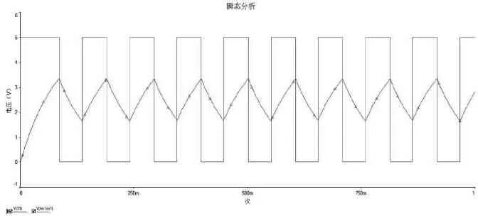
Figure 3 Timer
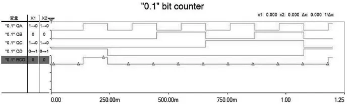
Figure 4 “0.1” second bit counter
2.1 Switches for turning on/off,reset,and pause
Single-pole double-throw switches(SPDT)are used as switches in this project.The working principle of SPDT is like this:The two parallel row of three pins of the six-pin SPDT has the same voltage level.Each side of the switch has the same conceptual structure with the above graph -the middle pin is always connected while the two sides can be switched to decide which side to be connected with themiddle pin and its connected pathway.
For turning on/off,when the VCC power supply in connected to the ground rather than the other pathways that should be connected with power in the circuit,all the power is cut off in this circuit.For reset switch of the first two-bit counter,the switch is directly connected with their “CLR”pins.This is easy to understand because the “CLR”is low-active,in normal condition it should connect high(VCC)but only clear the screen when connected with low(ground).While for the last bit counter in the left,the VCC input of the AND gate is connected with the switch.For pause,a SPDT connects the trigger pin of the 555 timer and the ground serving as the “pause” switch.This is because the working principle of the “TRI” pin of 555 timer is that when it is connected to low(ground),the timer will stop working thus cannot generate the clock signal anymore.
2.2 Buzzer
A buzzer which can ring every half minutes is connected as shown in Figure 5.
Due to the decoder which consists of logic gates including inverter,AND gate and NAND gate,the input signal of buzzer is ensured to be high each time when counter reach 29 or 59(ignore the least bit counter here),and ring for one second.
2.3 Deceleration and Acceleration
A SPDT connects all the other pins that should be connected with the capacitor with either capacitor one or capacitor two serves as the “speed-shifting” switch as shown in the blue circle in Figure 6.
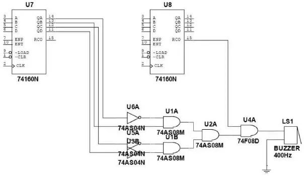
Figure 5 Buzzer

Figure 6 Speed Shifting
As discussed previously,the capacitance of the capacitor that connected with “DIS” pin of timer can control the frequency of the clock signal,therefore,by changing the capacitor,the counting speed of this circuit will change.In this case,the “speed-shifting”switch can switch from the two available capacitors with 1µF and 10µF respectively which can result in a counting speed of 1 second or 0.1 second of the fastest counter.
3 Conclusion
The common used IC chips such as 74160,7447,AND/NAND/NOT gates were utilized effectively in this experiment.The working principle of these chips were also comprehensively learnt.The circuiting and wiring ability was practiced fully after finish the manual construction of this stopwatch circuit.The simulation software like Multisim and PSPICE were effectively used in this lab to help the design of circuit as well.
[Reference]
[1]Texas Instrument Incorporated.“SN54160 THRU SN54163,SN54LS160A THRU SN54LS163A,SN54S162,SN54S163,SN74160 THRU SN74163,SN74LS160A THRU SN74LS163A,SN74S162,SN74S163 SYNCHRONOUS 4-BIT counters,SDLS060[M].Texas:Texas Instrument,1988.
[2]Renesas.HD74LS00 Quadruple 2-Input NAND Gates[Z]Japan:Renesas,2005.
[3]7-segment Display[EB/OL].(2016-10-10)[2011-11-21].http://www.electronics-tutorials.ws/blog/7-segment-display-tutorial.html.
[4]NA555,NE555,SA555,SE555PRECISION TIMERS[J].Texas:Texas Instrument,2006.
[5]555 timer[EB/OL].(2016-10-10)[2012-09-28].http://www.kpsec.freeuk.com/555timer.htm.
多功能电子钟的设计与搭建
赵睿敏
(英国利物浦大学,英国 利物浦 L693BX)
这篇文章旨在记录一个电子钟项目的完成过程。这个项目的目标是建造一个搭建在面包板上的电子钟的电路使其能用两个计时器来准确计时1分钟。项目的最终成果是这个电子钟成功包含了3个计时器以及一系列附加功能,比如蜂鸣器、计时速度改变功能,以及计时重置功能。这些功能都用软件模拟成功并且搭建成功了。主要器件有74160,7447等集成电路模块。未来的提高方向是改良电子钟的外观和合理实用性。
电子钟;555计时器;逻辑电路;IC;Multisim;PSPICE
Author introduction:Zhao Ruimin(1995—),Female,Shandong Jinan,Undergraduate;Research field:Telecommunication.