Effects of precursor solution concentration on dielectric properties of (Pb, La)(Zr, Ti)O3 antiferroelectric thick films by sol-gel processing*
2013-11-01LVYongbo吕永博GUOMaoxiang郭茂香GUANXinfeng关新锋CHOUXiujian丑修建ZHANGWendong张文栋
LV Yong-bo(吕永博), GUO Mao-xiang(郭茂香), GUAN Xin-feng(关新锋),CHOU Xiu-jian(丑修建), ZHANG Wen-dong(张文栋)
(Key Laboratory of Instrumentation Science & Dynamic Measurement(North University of China),Ministry of Education, Taiyuan 030051, China)
Effects of precursor solution concentration on dielectric properties of (Pb, La)(Zr, Ti)O3antiferroelectric thick films by sol-gel processing*
LV Yong-bo(吕永博), GUO Mao-xiang(郭茂香), GUAN Xin-feng(关新锋),CHOU Xiu-jian(丑修建), ZHANG Wen-dong(张文栋)
(Key Laboratory of Instrumentation Science & Dynamic Measurement(North University of China),Ministry of Education, Taiyuan 030051, China)
Pb0.97La0.02Zr0.95Ti0.05O3(PLZT) antiferroelectric thick films derived from different precursor solution concentrations are prepared on platinized silicon substrates by sol-gel processing. The films present polycrystalline perovskite structure with a (100) preferred orientation by X-ray diffraction (XRD) analysis. The antiferroelectricity of the films is confirmed by the double hysteresis behaviors of polarization and double-bufferfly response of dielectric constant under the applied electrical field. Antiferroelectric properties and dielectric constant are improved while the polarization characteristic values are reduced with the increase of precursor solution concentration. The films at higher precursor solution concentration exhibit excellent dielectric properties.
engineering ceramics; precursor solution concentration; microstructure; antiferroelectric thick film
Antiferroelectric materials display the different electric-field induced phase transformations from antiferroelectric to ferroelectric (AFE-FE) for the unique microstructure, and the phase transition process can be induced by the temperature and stress. In fact, compared with other antiferroelectric thin films or antiferroelectric ceramic, lead lanthanm zirconate titanate antiferroelectric thick films hold the properties, such as simpler composition, easier preparation and lower price. Antiferroelectric materials have the potential applications in energy storage, high-strain transducers/actuators and tunable pyroelectric thermal sensors due to the remarkable change of polarization, strains and current during the AFE-FE transition. In recent years, there are many reports on AFE materials, such as (Pb, Zr)O3(PZ), (Pb, La)(Zr, Sn, Ti)O3(PLZST) and PbNb (Zr, Sn, Ti) O3(PNZST)[1-3]. (Pb, La)(Zr, Ti)O3antiferroelectric materials are a kind of typical antiferroelectric system, but the research on this kind of antiferroelectric thick films is relatively less. (Pb, La)(Zr, Ti)O3thick films which possess lower driving voltage, higher renitency strength, larger storage energy and smaller volume have shown great potential in the areas of high charge storage devices, microelectronic and micro-electromechanical systems (MEMS) with the development of the fabrication technology[4].
There are many ways for the preparation of (Pb, La)(Zr, Ti)O3antiferroelectric thick films, such as the sol-gel method (Sol-Gel), sputtering (Sputtering) and pulsed laser deposition (PLD)[5-10], and so on. Sol-gel processing has advantages such as low cost, excellence in composition control even for multiple-cation systems, homogeneity with large area coverage, capability of building up films with several micrometers thick, and compatibility with many semiconductor-fabrication technologies[11], hence, most antiferroelectric films for heterogenous integration are prepared by sol-gel processing. The precursor solution, catalyst, complex agent, drying control agent and so on are the important factors of sol-gel processing. One precursor solution is the basis of high quality antiferroelectric films production. The effects of precursor solution concentration on microstructure, density and electrical performance for antiferroelectric films are great.
In this paper, Pb0.97La0.02Zr0.95Ti0.05O3(PLZT) antiferroelectric thick films were fabricated on Pt(111)/Ti/SiO2/Si(100) at different precursor solution concentrations of 0.3 mol/L, 0.4 mol/L and 0.5 mol/L, respectively, via sol-gel processing. The effects of precursor solution concentration on the structure, phase transformation behaviors and electric properties of the films were investigated.
1 Experimental details
PLZT antiferroelectric thick films were prepared by sol-gel method on Pt(111)/Ti/SiO2/Si(100) substrates. The raw materials were lead acetate trihydrate [Pb(CH3COO)2-3H2O], lanthanum acetate [La(CH3-COO)3], zirconium propoxide [Zr(OC3H7)4] and titanium isopropoxide [Ti[OCH(CH3)2]4]. Acetic acid was selected as a solvent. According to the predetermined number, lead acetate trihydrate with 10% excess to compensate Pb loss, lanthanum acetate hydrate and acetic acid mixed in needed ratio was distilled at 110 ℃ for 1 h. When the mixed solution was cooled to room temperature, zirconium propoxide and titanium isopropoxide were added and mixed for 30 min. At the same time, distilled water was added in order to stabilize the solution. Lactic acid was added into the solution as catalyzer and chelation in the proportion of one mole of lactic acid to one mole of lead. Finally, the solution was adjusted to 0.3 mol/L, 0.4 mol/L and 0.5 mol/L (samples A, B and C) using the acetic acid. Then PLZT thick films were grown on Pt/TiO2/SiO2/Si substrates by spin-coating method. A lead oxide buffer layer prepared from lead acetate trihydrate was deposited on the platinum electrode by annealing at 700 ℃ for 30 min. Each PLZT layer was spin coated at 3 000 rpm for 20 s and pyrolyzed at 300 ℃ and 600 ℃ for 10 min, respectively. The spin coating and heat-treatment were repeated several times to obtain the desired thickness. At last, a capping layer of lead oxide was added to prevent Pb from volatilization and the films were annealed at 700 ℃ for 30 min to form the perovskite phase. The final thicknesses of all the films were obtained about 1 215 nm from Fig.1. Gold pads of 0.50 mm in diameter were obtained on the film surface as top electrodes by DC sputtering for electrical measurement.
The phase characterization and microstructure of PLZT thick films were examined by Bruker D8 advance X-ray diffractometer and atomic force microscope (AFM), respectively. The field-induced hysteresis loops of the PLZT thick films were tested by a modified Sawyer-Tower circuit. The temperature and field dependent dielectric properties of the PLZT thick films were measured by an Agilent 4284A LCR meter.

Fig.1 Cross-section SEM images for PLZT thick films
2 Results and discussion
XRD patterns of PLZT antiferroelectric thick films are shown in Fig.2.

Fig.2 XRD patterns of PLZT antiferroelectric thick films with different precursor solution concentrations
It is clearly seen that all the films are polycrystalline perovskite structure and present highly preferred-(100) orientation. The (100)-preferred orientation of the films can be caused by the presence of (001)-oriented PbO buffer layer. The (001)-oriented PbO crystals on the surface of the platinum electrode provide nucleation sites for the overlaid PLZT films and enhance the formation of their (100) orientation[12]. In order to study the effects of precursor solution concentration on the orientation of thick films, the (100)-orientation factor was described by the following equation[13]:

(1)
According to Eq.(1), the (100) orientation factor of the thick films were 0.85, 0.88 and 0.92, respectively, which indicates that (100)-preferred orientation increases with the increase of precursor solution concentration. Highly preferred-(100) orientation means that the nucleation of the PLZT films is weakly controlled by the substrate effect[14].
Fig.3 shows the surface morphology of PLZT antiferroelectric thick films with different precursor solution concentrations.
From Fig.3, it can be seen that the films are smooth, dense and uniform with average grain sizes of about 80 nm, 120 nm and 200 nm, respectively, which suggests that all the films are of good qualities. The grain sizes and the density of the films grow with the increase of the precursor solution concentration, which exactly accords with the enhanced trend of the orientation.

Fig.3 AFM images of PLZT antiferroelectric thick films at different precursor solution concentration
Fig.4 shows the polarizations (P-E) loops of PLZT antiferroelectric thick films at different precursor solution concentrations, which were measured at the frequency of 100 Hz and with a maximum applied voltage of 60 V.

Fig.4 Hysteresis loops of PLZT antiferroelectric thick films at different precursor solution concentrations
The P-E loops of the films which display typical double hysteresis loop are square-like, representing an abrupt change in polarization and a sharp phase transition between AFE and FE phases. The switching field could be obtained by two steepest sections of the hysteresis loops and the corresponding values are determined by the intersections of the slope and the horizontal axis. The forward AFE-FE phase transition fields and backward FE-AFE phase transition fields are 162 kV/cm, 186 kV/cm, 209 kV/cm and 73 kV/cm, 95 kV/cm, 117 kV/cm, respectively. Obviously, AFE-FE(EF) and FE-AFE(EA) phase transition fields gradually increase with the increase of concentration. This can be attributed to the higher film density[8]. However, the saturation polarization (Pmax) of the films are 56 μC/cm2, 47 μC/cm2and 38 μC/cm2, as the precursor solution concentration increases from 0.3 mol/L to 0.5 mol/L. Additionally, unlike antiferroelectric ceramic blocks (the residual polarizations are zero), there are a!small amount of remnant polarization (Pr) in the samples which might be due to leakage current and substrate stress, decreasing with increasing concentration. The reduction of Pmaxand Prmay be result from combinative effects of (100)-preferred orientation and lattice distortion[14].
The dielectric constant and loss of PLZT antiferroelectric thick films in DC field are shown in Fig.5. The mode of measurement was conducted in this way: 0 to Emax, then Emaxto -Emax, and -Emaxto 0. The test frequency was 100 kHz.
It can be seen from Fig.5 that the films present double-butterfly C-V curves. The phase transition field equates to the electric field corresponding to the peak of dielectric constant. The forward AFE to FE and reverse FE to AFE transition fields are about 192 kV/cm, 204 kV/cm, 223 kV/cm and 123 kV/cm, 133 kV/cm, 149 kV/cm for sample A, B and C, respectively (Fig.5(a)). The increasing phase transition fields show more stable antiferroelectricity of the films at higher concentration. The results demonstrate that the forward and reverse switching fields from the C-V analysis are in close agreement with the P-E measurements on the same sample. Difference of these measured data on C-V and P-E curves may result from two different measurement mechanisms. The increase in dielectric constant and decrease in dielectric loss (Fig.5(b)) of the films can be easily related to the variation of film density and grain sizes at ascending precursor solution concentration. That is because rising grain sizes reduce the volume fraction of grain boundaries and make the domain wall motion easier[15].
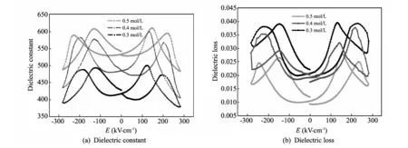
Fig.5 Dielectric constant and dielectric loss of PLZT antiferroelectric thick films at different precursor solution concentrations as a function of DC field
Fig.6 shows the dielectric constant and dielectric loss of PLZT antiferroelectric films at different precussor solution concentrations, as a function of temperature under the frequency of 1 kHz. The phase transition about AFE to paraelectric (PE) but no AFE-FE is observed during the heating process. It can be seen that the Curie temperature was 217 ℃, 221 ℃ and 223 ℃, respectively(Fig.6(a)). The tiny shift in Curie temperature could be explained by rising stress along with film density. As expected, the dielectric constant increases, but loss decreases as precursor solution concentration changes from 0.3 mol/L to 0.5 mol/L(Fig.6(b)), which also owes to the increase in film density and grain sizes.

Fig.6 Temperature dependence of dielectric constant and dielectric loss of PLZT antiferroelectric thick films at different precursor solution concentrations
3 Conclusion
PLZT antiferroelectric thick films of about 1.2 μm at different precursor solution concentrations were deposited on Pt(111)/Ti/SiO2/Si(100) substrates by the sol-gel processing. The dependence of microstructure and electrical properties as a function of precursor solution concentration (0.3 mol/L, 0.4 mol/L and 0.5 mol/L) was observed in these films. The results indicate that all the films exhibit good quality with a (100)-preferred orientation and the orientation can be enhanced with the increase of the concentration. The P-E hysteresis loops of square-like illustrate that the antiferroelectric films are suitable for energy storage capacitor and high-strain transducers/actuator applications. Dielectric properties show that higher precursor solution concentration enhances the phase transition field and dielectric constant while reduces the dielectric loss, the saturation polarization and remnant polarization, which can be attributed mainly to in terms of crystallographic orientation, film density and grain sizes.
[1] Bittner R, Humer K, Weber H W, et al. Radiation-induced defects in antiferroelectric thin films. Fusion Engineering and Design, 2003, (66-68): 833.
[2] HAO Xi-hong, ZHAI Ji-wei. Low-temperature growth of (110)-preferred Pb0.97La0.02(Zr0.88Sn0.10Ti0.02)O3antiferroelectric thin films on LaNiO3/Si substrate. Journal of Crystal Growth, 2008, 310: 1137-1141.
[3] ZHAI Ji-wei, CHEN Huan-bei, Colla E V, et al. Direct current field adjustable ferroelectric behaviour in (Pb, Nb)(Zr, Sn, Ti)O3antiferroelectric thin films. Journal of Physics: Condensed Matter, 2003, 15(6): 963.
[4] Bharadwaja S S N, Krupanidhi S B. Dielectric relaxation in antiferroelectric multigrain PbZrO3thin films. Materials Science and Engineering B, 2000, 78(2/3): 75-83.
[5] XU Bao-ming, YE Yao-heng, WANG Qing-ming, et al. Dependence of electrical properties on film thickness in lanthanum-doped lead zirconate titanate stannate antiferroelectric thin films. Journal of Applied Physics, 1999, 85(7): 3753-3758.
[6] ZHAI Ji-wei, LI Xia, CHEN Huan-bei. The behaviours of ferroelectric and antiferroelectric in PNZST thin films for different orientation. Thin Solid Films, 2004, 446: 200-204.
[7] Yamakawa K, Gachigi K W, Trolier-mckinstry S, et al. Structural and electrical properties of antiferroelectric lead zirconate thin films prepared by reactive magnetron co-sputtering. Journal of Materials Science, 1997, 32(19): 5169-5176.
[8] XU Zheng-kui, CHAN Wai-hong. Preparation and electrical properties of highly (111) oriented antiferroelectric PLZST films by radio frequency magnetron sputtering. Acta Materialia, 2007, 55(11): 3923-3928.
[9] Parui J, Krupanidhi S B. Dielectric properties of (110) oriented PbZrO3and La-modified PbZrO3thin films grown by sol-gel process on Pt(111)/Ti/SiO2/Si substrate. Journal of Applied Physics, 2006, 100(4): 044102-044110.
[10] YE Yao-heng, ZHAI Ji-wei, CHEN Huan-bei. Dielectric properties of lead lanthanum zirconate stanate titanate antiferroelectric thin films prepared by pulsed laser deposition. Journal of Applied Physics, 2004, 95(11): 6341-6346.
[11] XU Bao-min, Cross L E, Bernstein J J. Ferroelectric and antiferroelectric films for microelectromechanical systems applications. Thin Solid Films, 2000, 377/378: 712-718.
[12] GONG Wen, LI Jing-feng, CHU Xiang-cheng, et al. Preparation and characterization of sol-gel derived(100)-textured Pb(Zr,Ti)O3thin films: PbO seeding role in the formation of preferential orientation. Acta Materialia, 2004, 52(9): 2787-2793.
[13] YU Jian, Meng X J, Sun J L, et al. Optical and electrical properties of highly(100)-oriented PbZr1-xTixO3thin films on the LaNiO3buffer layer. Journal of Applied Physics, 2004, 96(5): 2792-2799.
[14] Zhang S Q, Wang L D, Li W L, et al. Effects of lanthanum doping on the preferred orientation, phase structure and electrical properties of sol-gel derived Pb1-3x/2Lax(Zr0.6Ti0.4)O3thin films. Journal of Alloys and Compounds, 2011, 509(6): 2976-2980.
[15] Kong L B, Ma J. Preparation and characterization of antiferroelectric PLZT2/95/5 thin films via a sol-gel process. Materials Letters, 2002, 56(1/2): 30-37.
date: 2013-02-27
National Natural Science Foundation of China(No. 60806039, No. 51175483); China Postdoctoral Science Foundation Projects (No. 20090461275, No. 201003658); Shanxi Provincial Natural Science Foundation of China(No. 20100210023-6) and Shanxi Provincial Young Leaders on Science.
CHOU Xiu-jian (chouxiujian@nuc.edu.cn)
CLD number: TB34 Document code: A
1674-8042(2013)03-0294-05
10.3969/j.issn.1674-8042.2013.03.020
杂志排行

Journal of Measurement Science and Instrumentation的其它文章
- Impact of low temperature on smartphone battery consumption*
- Roll angle measurement system based oni triaxial magneto-resistive sensor*
- Dynamic test methods for natural frequency of footbridge*
- High-speed broadband data acquisition system based on FPGA*
- Method of military software security and vulnerability testing based on process mutation*
- Study on denoising filter of underwater vehicle using DWT*