High-speed broadband data acquisition system based on FPGA*
2013-11-01LIUJunzhi刘军智
LIU Jun-zhi (刘军智)
(Science and Technology on Electronic Test & Measurement Laboratory, Qingdao 266555, China)
High-speed broadband data acquisition system based on FPGA*
LIU Jun-zhi (刘军智)
(Science and Technology on Electronic Test & Measurement Laboratory, Qingdao 266555, China)
A field-programmable gate array (FPGA) based high-speed broadband data acquisition system is designed. The system has a dual channel simultaneous acquisition function. The maximum sampling rate is 500 MSa/s and bandwidth is 200 MHz, which solves the large bandwidth, high-speed signal acquisition and processing problems. At present, the data acquisition system is successfully used in broadband receiver test systems.
high-speed data acquisition; FPGA; wideband; cross collection; data combination
0 Introduction
With the development of wireless communication and computing technology[1], signal compressing and analyzing technology, the signals from military affairs or satellite communication are developing to high frequency, broad band and digital ones. Thus high-speed data acquisition devices become important components of the whole system and are widely used in the areas of radar, communication, earthquake exploring, intelligent instrument, scientific experiments, etc.[2].
Data acquisition is an effective means of information acquisition. As an important branch of information science, data acquisition technology is an integrated application technology. How to collect and store high-speed signals in real-time in order to avoid being lost and to meet the requirements of work site is always a hot topic in high-speed data acquisition system research.
This paper takes test occasions such as target imaging, near-field scanning, etc. as the background. Modern radio receiver systems are utilized to capture a large number of high-speed real-time signals[3]. Because low-speed narrow-band low-resolution data acquisition systems usually can not meet the demands of testing[5], this paper introduces a data acquisition system with 500 MSa/s sampling rate, 200 MHz bandwidth and 16-bit resolution. The high-speed data acquisition and processing system is designed based on field-programmble gate array (FPGA) and digital signal processing (DSP) technology, which uses peripheral component interconnect (PCI) local bus.
1 Overall design of high-speed broadband data acquisition system
The structure of single channel high-speed broadband data acquisition system is shown in Fig.1, but the whole system is a dual channel one.
From Fig.1, it can be seen that the acquisition system consists of signal conditioning circuit, A/D conversion circuit, clock generation circuit, FPGA data pre-processing circuit, DSP control and data processing circuit and PCI interface circuit, and so on. Especially, each channel of the system uses two A/D convertors. All these respective components are corrdinated each other to complete the data acquisition and signal processing functions. At present, we usually integrate the accelerometer, gyroscope and the following signal processing circuit on a single chip. In the course of structure design, not only the factors of general accelerometer and gyroscope design need to be considered, but also the inertia sensitive components must work in the best area, thus these components are slightly influenced each other. Through theory analysis and structural simulation, this paper design a single chip integrated accelerometer gyroscope.
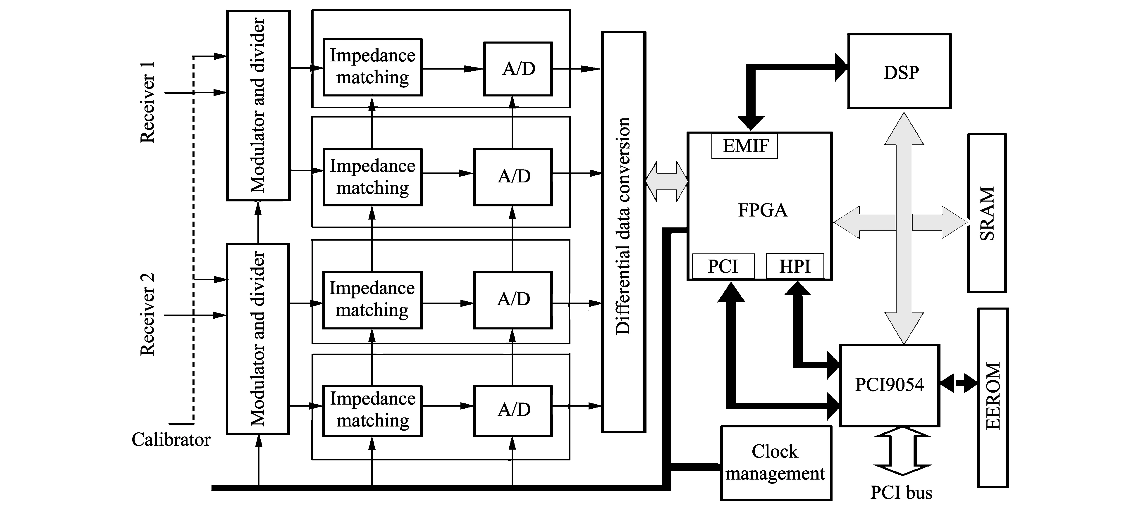
Fig.1 Block diagram of single channel data acquisition system
2 Key technologies of the system
2.1 Front-end pre-processing circuit
The main role of front-end pre-processing circuit is to send intermediate frequency (IF) signal of 375±100 MHz into the power divider circuit separately. Through flatness adjustment circuit and gain adjustment circuit, the modulated signal is divided into two signals. Then through impedance matching circuit, the signals are transmitted to A/D convertor (ADC)[6]. According to different gains, the signal through power divider selects different resistance values in impedance matching circuit to get a match. Here the single end differential conversion and A/D front-end amplifier are achieved by ADL5562, the impedance matching between ADL5562 and AD9467 needs to be determined based on the bandwidth of IF signal and the input impedance of sampling chip. The design of matching circuit will directly affect the signal-to-noise ratio (SNR) and spurious-free dynamic range (SFDR) of ADC. The specific implementation process is shown in Fig.2.

Fig.2 Block diagram of front-end pre-processing circuit
In order to keep consistence in dynamic range and flatness of input data from the four ADCs and ensure that there is no confusion about acquired data, we add external reference chips when we design ADC circuit. Because the added external reference chips need to drive 4-channel ADC, we choose chip REF3012 with maximum output current 25 mA. This chip can output 1.25 V reference voltage, as well as drive 4-channel ADC.
FPGA[7]data processing circuit is the core part of the data acquisition system, which controls the data acquisition, processing and transmission of the whole system. It will be introduced as follows.
2.2 FPGA-based high-speed broadband IF processing circuit
The work frequency of sampling chip is very high, so a differential clock is needed. If the differential clock outside the system is adopted, it may cause high noise resulting in sampling chip not working properly or poor signal. So we choose inner clock management chip of the system to provide clock signal. As the clock management chip uses three lines of serial peripheral interface (SPI), FPGA needs to control not only SPI to satisfy the timing requirements, but also the output clock phase to guarantee clock phase difference of 180 degrees of two channels[8].

Fig.3 Block diagram of FPGA-based data processing circuit
After A/D conversion, the high-speed differential data stream is sent directly to the high-speed FPGA. In FPGA, differential signal will be converted into a single-end signal to facilitate follow-up treatment. Here we directly call IP core, that is, ISE software, which is developed by X Co.[9]and can convert the differential data and clock into single-end data and clock for easy signal processing. And then through the spin-down, two-way data is combined to be one-way data. The low rate data stream uses the quadrature two-way numerical controller oscillator (NCO) to achieve digital down conversion. After digital filtering processing, the baseband information carried by IF is removed, and then it is saved to the inner FPGA memory. Block diagram of FPGA data processing is shown in Fig.3.
In high-speed clock processing, burr and jitter are prone to produce, which have great harm to high-speed data processing and might even collect error data. In order to eliminate jiter, a special digital clock manager (DCM) for high-speed data acquisition is used. There are 18 DCMs to be used, which can realize phase shift, flexible frequency synthesis, etc. Thus different feedback modes can meet the requirements of acquisition and subsequent processing of the clock.
For 250 MHz data stream that needs to be processed directly, it is very difficult to create and hold time. Through the speed reduction processing module, high-speed data of each channel is converted into 62.5 MHz, 64 bit data, and it is convenient for the subsequent transmission, storage and processing. The inner clock flow is shown in Fig.4.

Fig.4 Block diagram of inner clock flow
Digital filter plays an important role in digital signal processing. It is widely used as a basic linear processing module. It can realize accurate linear phase characteristics which the analog device is difficult to achieve. Digital filter is divided into infinite impulse response filter (IIR) and finite impulse response filter (FIR). Under the same conditions, the operation speed of FIR filter is faster than that of the IIR filter. Meanwhile FIR filter has the advantages of no feedback loop, simple structure and strict linear phase, etc. Thus under the conditions of more stringent phase requirements, we often use FIR digital filter. Here we first use filter design toolbox in Matlab to select low-pass filter model. After selecting the appropriate starting and ending frequency, we observe amplitude frequency and phase frequency characteristics till meeting the design goals. And then tap coefficients of the designed filter are obtained and rounded up as well as codes are stored. At last, by using inner FIR filter of FPGA, the corresponding order of filters is set. The filter coefficients use the files generated by Matlab.
The data after digital filtering includes a lot of clutter and unnecessary data. Thus we need a truncate approach to select the useful data.
2.3 Multi-channel LVDS data receiving and storage technology
Since the digital output of ADC is low voltage differential signaling (LVDS) multiplexer parallel[11]data flow and its maximum sampling rate reaches 500 Msa/s, how to deal with multi-channel LVDS signal is the key. In FPGA, by simulation, optimization, timing constraints and DCM phase adjustment, etc. error-free data is received and then the differential signal is converted into a single-end signal by FPGA logic core. Meanwhile a deceleration processing method is used for signal storage.
Since FPGA chip XC5VSX95T has inner block RAM of 8 Mbit, but the system target requires the longest sampling period of 1 ms, sampling rate of 500 MHz and the maximum storage data of only 2 Mbit, we need the inner logical resources to get the data access. On the one hand, on-chip memory is easy to control, on the other hand, reducing the external complex circuit can make the acquisition system volume as small as possible.
2.4 Multi-channel synchronous technology
In order to ensure the strict synchronization of the two channels, hardware approach and software approach are combined to make each differential clock linearly and strictly equal length in the iardware design, and clock generation circuit can adjust the brightest clock. Buu due to traces of difference and latent consistency of device itself, it is difficult to strictly control the hardware. Here we use software compensation method to set inner delay of precision adjustment clock management chip. By continuously adjusting the phase relationship among the clocks, the strict synchronization between two channels is achieved.
The phase shift can be got by changing the phase shift value, as described by
clkinperiod×360,
(1)
where the measurement unit of plase shift is degree.
In FPGA, we use the counter to construct a delay control module to adjust phase shift. By setting different values for the counter, we can make the phase change within 0 to 360 degree. Because of the limitation of the device itself, the clock cycle we input to DCM is 2 ns.
The main role of clock generation circuit is to produce 4-way high-speed differential clocks. In order to control each channel between the two A/D sampling clocks to invert relationship for easy data stitching, we choose clock management chip AD9516-5, which is combined with vector-controlled oscillator (VCO) to construct the inner phase locked loop (PLL) synthesizer chip. Through the inner divider circuit, it can output 4-channel differential clocks, and each clock can adjust the phase between any two differential channels. The output frequency can reach 800 MHz, which fully meets the requirements of the project. Fig.5 is the received data with chip scope observation.
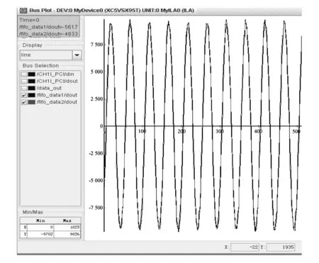
Fig.5 Synchronous received data
2.5 Digital amplitude and phase compensation technology
The inconsistencies in the amplitude and phase of the phase delay directly affect the results of the measurement when the two signals deviate from their true values. Retardation deviations relate to not only the amplitude inconsistent parameters, but also the initial phase of the signal. For amplitude inconsistency, we adopt the gain compensation method to compensate for signal inphase and quadrature component of the gain. For the inconsistency of the phase, we divide a received signal of each channel into quadrature and in-phase components. After gain processing, they are combined into one signal to eliminate the impact of phase inconsistencies.
3 Test results
Test results show that the designed high-speed broadband data acquisition system meets the pre-design requirement, and the system has a higher dynamic range. The graph of the measured IF bandwidth of 200 MHz is shown in Fig.6. The test results of dynamic range and receiver' sensitivity are shown in Table 1.
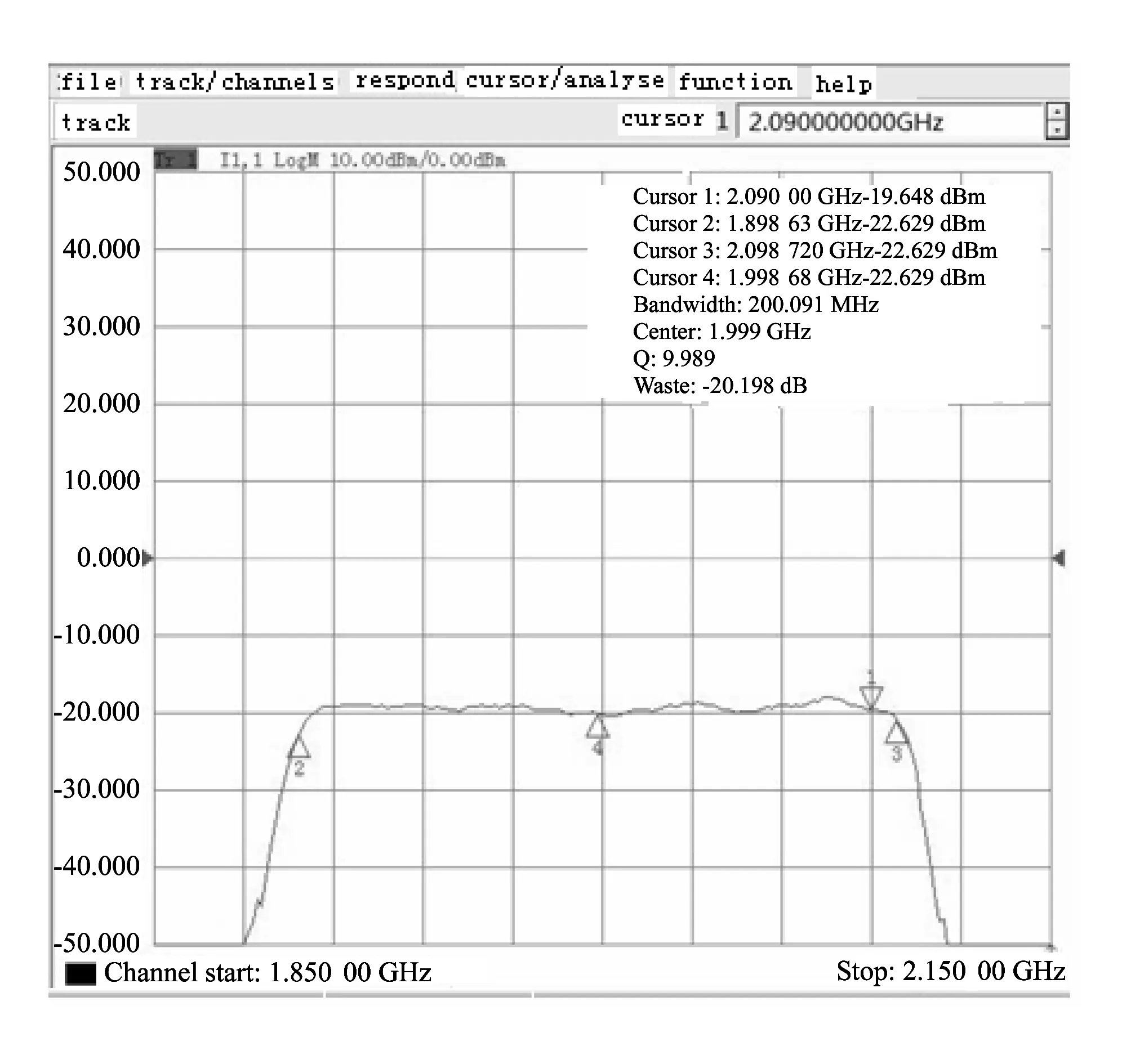
Fig.6 Measured 200 MHz IF bandwidth curve
Table 1 Test results

TestitemTheoryvalueTestresultDynamicrange70dB73dBReceiver'ssensitivity-90dBm(800MHz)-95.30dBm-90dBm(2GHz)-95.40dBm-90dBm(10GHz)-97.5dBm-90dBm(20GHz)-96.4dBm-90dBm(40GHz)-95.3dBm
4 Conclusion
In this paper, the designed FPGA-based high-speed broadband data acquisition system can handle the signal bandwidth with sampling rate up to 200 MHz.The high stability of the data acquisition system[10]make it can be applied to the broadband receiver system.
[1] ZUO Zhen-ping, LI Li-gong. Digital communication measuring instruments. Beijing: the People's Posts and Telecommunications Press, 2007: 434-435.
[2] ADI University Programs. High-speed design technology. Beijing: Publishing House of Electronics Industry, 2010: 123-158.
[3] YANG Xiao-niu, LOU Yi-cai, XU Jian-liang. Software radio principles and application. Beijing: Publishing House of Electronics Industry, 2001: 83-173.
[4] Giannonea L, Cernab M, Colec R, et al. Data acquisition and real-time signal processing of plasma diagnostics on ASDEX upgrade using LabVIEW RT. Fusion Engineering and Design, 2010, 85: 303-307.
[5] POZNIAK K T. FPGA-based specialized trigger and data acquisition systems for high-energy physics experiments. Measurement Science and Technology, 2010, 21(6): 26-29.
[6] Analog Devices. Analog devices (ADI) AD5446 user manual. 2012.
[7] WANG Zhen-hong. FPGA development and application. Beijing: Tsinghua University Press, 2010: 1-47.
[8] LIU Hai-bo, LONG Teng, ZENG Da-zhi. Design of a two-channel ultra high frequence data acquisition system based on FPGA. In: Proceedings of 2006 CIE International Conference on Radar, London, 2007: 1263-1268.
[9] Xilinx Inc. Virtex-5 libraries guide for schematic designs. UG622(v12.2). 2010.
[10] ZHANG Bao-feng, WANG Ya, ZHU Jun-chao. Design of high speed data acquisition system based on FPGA and DSP. In: Proceedings of International Conference on Artifical Intelligence and Education, Hangzhou, China, 2010: 132-135.
[11] Baklouti M, Aydi Y, Abi M. Scalabie mpNoC for massively parallel-design and implementation on FPGA. Journal of Systems Architecture, 2010, 56(7): 9-15.
date: 2013-03-05
LIU Jun-zhi (ljz6221@163.com)
CLD number: TP274+.2 Document code: A
1674-8042(2013)03-0223-05
10.3969/j.issn.1674-8042.2013.03.005
杂志排行

Journal of Measurement Science and Instrumentation的其它文章
- Impact of low temperature on smartphone battery consumption*
- Roll angle measurement system based oni triaxial magneto-resistive sensor*
- Dynamic test methods for natural frequency of footbridge*
- Method of military software security and vulnerability testing based on process mutation*
- Study on denoising filter of underwater vehicle using DWT*
- Obstacle detection using multi-sensor fusion*