Transient Analysis of InGaN/GaN Light-emitting Diode with Varied Quantum Well Number
2013-10-21CHENGuichuFANGuanghan
CHEN Gui-chu,FAN Guang-han
(1.Institute of Optoelectronic Material and Technology,South China Normal University,Guangzhou 510631,China;2.Department of Physics,Zhaoqing University,Zhaoqing 526061,China)
1 Introduction
The visible Ⅲ-nitride light-emitting diodes(LEDs)have received much attention due to their wide applications in full-color display,liquid crystal display back-lighting,mobile platforms,and illumination[1-4].High-luminescence and high-efficiency blue/green InGaN LEDs,especially,are of foremost importance for application in illumination market such as outdoor display and solid-state lighting.Up to now,most investigations focus on improving their static illuminant performance including the light extraction efficiency,however,few theoretical and experimental investigations have been reported on the dynamic response of InGaN LEDs,except that Shi and his co-workers have made an experimental study about the modulation properties of single LED and three cascade LEDs for the application in plastic optical fiber communication[5-6].
In this paper,a set of rate equations,which describe the dynamics of carriers and photons in In-GaN LED respectively,are casted in a circuit simulator SPICE by making use of standard circuit elements.The equivalent circuit model based on the rate equations is versatile in that it can be used to simulate the large-signal transient response.The performance of outpower versus current (P-I)is simulated to accord with the reported experimental P-I data by adjusting the parameters of rate equations.On the basis of the correct parameters,the transient response is simulated via the square current driving the equivalent circuit model.Furthermore,the rise time of optical output,derived from the transient response,is discussed by changing the number of quantum wells.
2 Rate Equations and Circuit Model
A green GaN-based LED with a 518 nm radiative wavelength,denoted as sample B in Ref.[5],is considered here.The quantum wells in active region are composed of 13.5 nm GaN barriers and 2.5 nm InGaN wells.Thus the dynamics of carriers and photons is described in terms of the following two nonlinear differential equations mentioned below[7],which form the basis of circuit model:
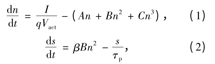
where n denotes the electron density (cm-3)in the active region;I is the injected current;q is the electronic charge;Vactis the volume of the active region;s is the photon density;β is spontaneous emission factor;τpis the lifetime of photon;A,B,and C are the non-radiative coefficient,radiative coefficient,Auger coefficient,respectively.The detailed expressions of Vactand β are given below[8]:
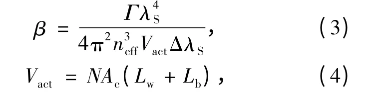
where Г is the confinement factor,neffis the effective refractivity,λSand ΔλSare peak wavelength and half-peak width,N is the number of quantum well,Acis the area of the cross section,Lwand Lbare the width of well and barrier,respectively.
In order to derive the equivalent-circuit representation from the rate equations (1)~(2),the standard circuit elements are brought to transform the rate equations into the specific type which suits the formation of circuit model.The non-radiative coefficient A is considered to be equal to 1/τnr,where τnris denoted as the non-radiative lifetime of carriers.Therefore the non-radiative recombination current Inis equal to qVactn/τnr,and the radiative recombination current and Auger recombination current are expressed as bI2nand cI3nrespectively,where b=B/(AqVact)2,c=C/(AqVact)3.The carrier population in the active region is also defined as:
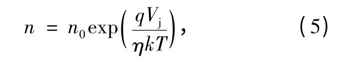
where n0is the equilibrium carrier density,Vjis the voltage across the active region,η is the corresponding diode ideality factor,typically set equaling to 2,T is the absolute temperature.The differential term qVactdn/dt of rate equation (1)can be denoted as a product of Cjand dVj/dt,with Cjexpressed as
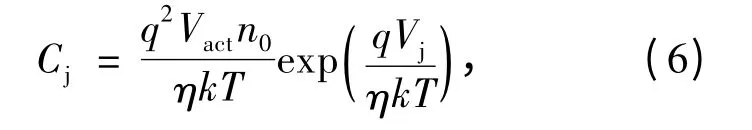
where Cjis a capacitance representing the charge storage effect in the active region.However,the type of equation (2)is not effective to form corresponding circuit model and improvements must be adopted to satisfy this requirement.The optical output power Pout[9]can be represented by a nodal voltage,namely:
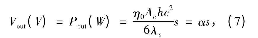
where η0is extracted light efficiency,the definition of Acand λsis referred to equations (3)~(4).With these modification,the rate equations (1)~(2)are transformed into the following type:
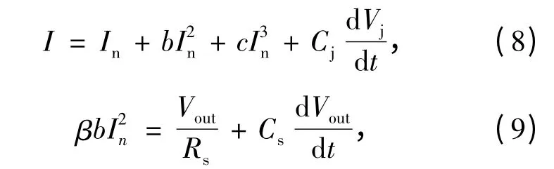
where Rs=ατp,Cs=1/α.The circuit model based on the equations (8)~(9)is formed in Fig.1.
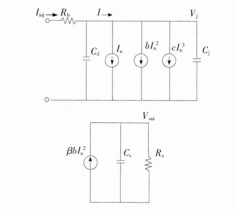
Fig.1 The equivalent circuit model of LED derived from rate equations
Iinjis the total injected current of LED with the parasitic elements Rband Cd,where Rbis considered to be equal to the differential resistance derived from the Shi's measured V-I curve[5],and Cdis a diffusion capacitance,which is added into the circuit model aiming to generalize the equation (8).Cd=C0(1-Vj/Vd)-1/2,where C0is the zero-bias diffusion capacitance,Vdis the diode built-in potential.In our simulations,C0is considered to be constant,but Rbis linearly changed with varied wells.
3 Simulation Results and Discussion
The equivalent circuit model of LED is a largesignal model,which is compatible with general purpose circuit simulators SPICE,and SPICE allows a circuit to contain resistors,capacitors,inductors,current dependent current/voltage sources,etc.The DC and transient analysis can be done based on the SPICE simulations.The values of the parameters used in our simulations are listed in Table 1[5,10-11].
Fig.2 shows the light-current characteristics of the sample B in Ref.[5].The squares represent the Shi's measured experimental data,and the curve is derived from the DC SPICE simulation of our circuitmodel.By adjusting the value of the model parameters A,B,C,and τp,our simulation results are very coincide with Shi's measured data.As shown in Fig.2,the simulated curve dips when the injected current is greater than 80 mA,which is due to the dominant Auger radiation with the large current injected into LED.
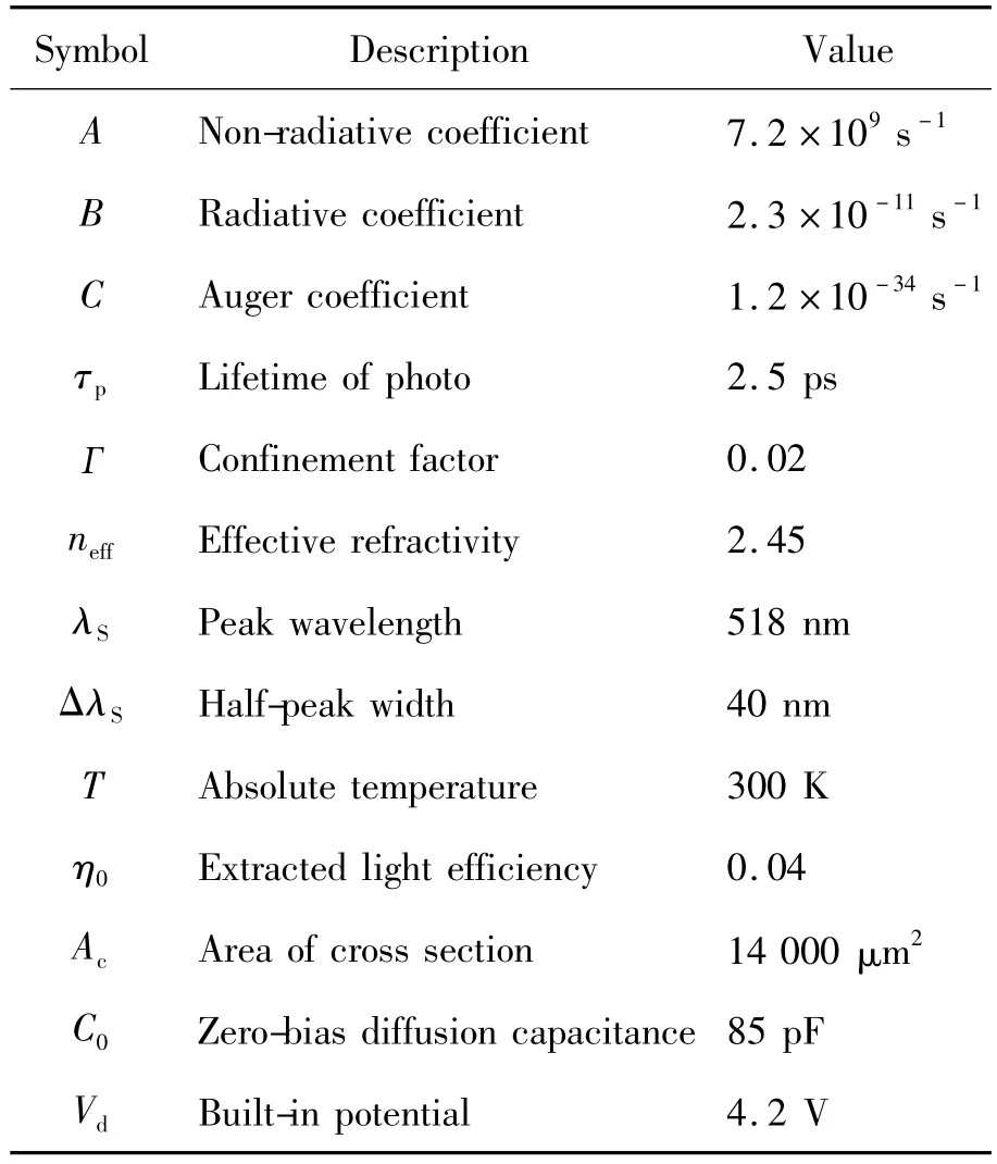
Table 1 Model parameters used in the simulation
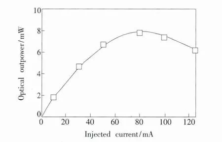
Fig.2 Output optical power vs.the injected current of sample B.Squares represent the Shi's measured experimental data.
Fig.3 shows the pulse response of InGaN LEDs with 2,4,and 6 wells in the active region,while a 50 mA-height square current is applicated at the time t=0 ns.The rise time tris determined as the time between 10% and 90% points of the light pulse.The rise time of Shi's sample B with 6 wells is calculated to be 7.8 ns,from the equation tr=0.35/f-3dB,where its-3 dB bandwidth is equal to 45 MHz.By adjusting the parameter C0,the rise time derived from transient simulation of SPICE model can be consistent with the calculated results mentioned above.
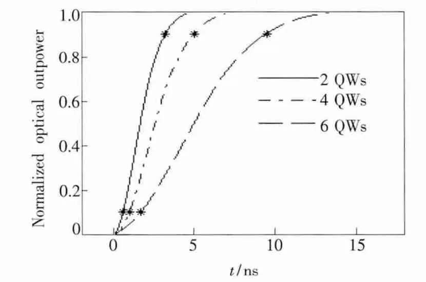
Fig.3 Transient response of GaN-based LED with 2,4,and 6 wells.
Fig.4 shows the relation between our simulated results of the rise time and the number of quantum wells.Two facts can explain why the rise time of light pulse increases with the number of wells.The rise time is governed by the injected carrier lifetime and the stored charge effect[12].Firstly,the increased volume of the active region will decrease the injected carrier density,which can affect the injected carrier lifetime.Secondly,from the equation(6),the charge stored capacitance Cjincreases with the volume,and then this will increase RbCjconstant of LED.
Fig.4 The simulated rise time vs.number of wells.Asterisk represents Shi's measured experimental result.
4 Conclusion
We have investigated the transient response of InGaN green LED with varied quantum wells on the basis of SPICE model.We find that the rise time increases with the number of quantum wells,which is also explained with two facts.Owing to the output power of LED enhanced with the number of wells,we propose that the optimized structure will be three wells in the active region,considering both the luminous power and the dynamic response.
[1]Shakya J,Knabe K,Kim K H,et al.Polarization of Ⅲ-nitride blue and ultraviolet light-emitting diodes[J].Appl.Phys.Lett.,2005,86(9):091107-1-3.
[2]Li J,Lin J Y,Jiang H X.Growth of Ⅲ-nitride photonic structures on large area silicon substrates[J].Appl.Phys.Lett.,2006,88(17):171909-1-3.
[3]Fan Y P,Cheng L W,Lin Y M,et al.Optimization of electrode shape for high power GaN-based light-emitting diodes[J].Optoelectron.Lett.,2009,5(5):0337-0340.
[4]Kim K S,Kim J H,Jung S J,et al.Stable temperature characteristics of InGaN blue light emitting diodes using AlGaN/GaN/InGaN superlattices as electron blocking layer[J].Appl.Phys.Lett.,2010,96(9):091104-1-3.
[5]Shi J W,Huang H Y,Sheu J K,et al.The improvement in modulation speed of GaN-based green light-emitting diode(LED)by use of n-type barrier doping for plastic optical fiber (POF)communication[J].IEEE Photon.Technol.Lett.,2006,18(15):1636-1638.
[6]Shi J W,Chen P Y,Chen C C,et al.Linear cascade GaN-based green light-emitting diodes with invariant high-speed power performance under high-temperature operation[J].IEEE Photon.Technol.Lett.,2008,20(23):1896-1898.
[7]Ryu H Y,Kim H S,Shim J I.Rate equation analysis of efficiency droop in InGaN light-emitting diodes[J].Appl.Phys.Lett.,2009,95(8):081114-1-3.
[8]Baba T,Hamano T,Koyama F,et al.Spontaneous emission factor of a microcavity DBR surface-emitting laser[J].IEEE J.Quan.Electron.,1991,21(6):1347-1358.
[9]Tsang W T.Semiconductor Injected Lasers and Light Emitting Diodes[M].Beijing:Press of Tsinghua university,1991.
[10]Yen S H,Tsai M C,Tsai M L,et al.Effect of n-type AlGaN layer on carrier transportation and efficiency droop of blue In-GaN light-emitting diodes[J].IEEE Photon.Technol.Lett.,2009,21(14):975-977.
[11]Kuo Y K,Tsai M C,Yen S H,et al.Effect of p-type last barrier on efficiency droop of blue InGaN light-emitting diodes[J].IEEE Quant.Electron.,2010,46(8):1214-1220.
[12]Suzuki A,Uji T,Inomoto Y,et al.InGaAsP/InP 1.3-μm wavelength surface-emitting LED's for high-speed short-haul optical communication systems[J].IEEE Transactions on Electron Device,1985,32(12):2609-2614.