An Investigation on a Tin Fixed Abrasive Polishing Pad with Phyllotactic Pattern for Polishing Wafer
2012-07-25LVYushan吕玉山LIUDianfei刘电飞KOUZhihui寇智慧
LV Yu-shan(吕玉山),LIU Dian-fei(刘电飞),KOU Zhi-hui(寇智慧)
(School of Mechanical Engineering,Shenyang Ligong University,Shenyang 110159,Liaoning,China)
Introduction
Polishing is currently a main processing method in the manufacturing fields of optic element,MEMS and IC.In a polishing process,a wafer is pressed against a rotating polishing pad while a polishing slurry,comprising some chemical agents and abrasive particles,is fed into a wafer-pad contact region,the material on workpiece surface is removed by the coupled chemicalmechanical interactions between the polishing pad and the workpiece surface.However,the polishing pad plays a very important role in polishing process,and the surface texture of polishing pad,such as shape of micropore,hole clearance,and arrangement of surface grooves,has an important effect on the contact pressure distribution,the temperature field,and the flow of polishing fluid[1].Therefore,the research on the texture and features of polishing pad has become a hot issue.Chiou Y C,Lee R T,and Yau C L[2]polished a wafer by using Al2O3abrasive which is continuously fixed by a composite electroforming tin on a copper disc,making the surface roughness beRa=2 nm,but the copper disc surface is continuous.Choi J Y and Jeong H D[3]produced a hydrophilic fixed abrasive polishing pad by using a screen printing method,which the fixed abrasive piece of the polishing pad is a matrix arrangement structure,and is used for polishing the mould and makes the surface roughness of polished mould beRa15.1 nm.Martin Kulawski[4]researched the polishing of MEMS microstructure with fixed abrasive polishing pad produced by 3M Company.The research results show that the planarization effects can be improved by using the protruding point structure of polishing pad which is of matrix distribution.Lee S,Hwang E and Keppeler C R[5]researched the design and fabricatring process of polishing pad with the macroscopic and microscopic matrix distribution of convex.This polishing pad is a double layer structure,of which one layer is a rigid polyurethane which contains abrasive,and the other one is a soft polyurethane which is a support part.The polishing experiments show that it can improve the effect of planarization.David B James[6]invented a fixed abrasive polishing system which is used for polishing wafer and disk substrates,the pad of this system uses a hydrophilic polyurethane fixed abrasive layer,which can ensure the slurry uniform flow and pH equalization in the polishing process and improve the uniformity of the surface material removal.Kim H Y[7]presented a kind of in-dressing polishing pad,which can assure that the material removal rate is constant in the polishing process.SU Jian-xiu,KANG Ren-ke,GUO Dong-ming, et al[8]studied a fixed-abrasive chemical-mechanical polishing technology for wafer in integrated circuit manufacturing,and according to the analysis of the polishing pad structure,polishing machine and polishing slurry,the merits of fixed abrasives CMP were presented.SHEN Liang-jian[9]studied a fixed abrasive polishing pad for micro-electronics manufacturing,designed the topography of fixed abrasive polishing pad of which the arrangement of fixed abrasive blocks is of matrix distribution,and manufactured the three-dimensional asperities on the pad by using silk screen printing.The polishing results show that,within a scanning area of 639 μm ×859 μm,the average roughness of wafers polished by fixed abrasive polishing pad and by conventional polishing method are 0.856 nm and 1.70 nm,respectively.The above researches have an important significance to improve the polishing effect.However,how to properly design the surface geometric structure of polishing pad and make polishing slurry flow field,contact temperature field and contact pressure field in contact interface be uniform are still the important problems to be approached.
Therefore,In order to achieve a better polishing effects,the surface geometric structure of the polishing pad is designed based on the phyllotaxis theory in the biology,and the fabricating methods of polishing pad are also discussed in this paper.
1 Phyllotaxis and Design and Fabrication of Polishing Pad
1.1 Phyllotactic Arrangement
Phyllotaxis,namely the arrangement of phylla(leaves,bracts,stickers,florets)on a plant’s surface,was intrigued the natural scientists before over four hundred years.These naturally occurring patterns provide a non-overlapping,optimal packing when the total number of nodes is not known a priori[10].Fig.1(a)shows the phyllotactic pattern of sunflower seeds,and Fig.1(b)shows the geometrical model of sunflower seed arrangements in polar coordinates.The phyllotactic patterns of sunflower seeds can be created according to H.Vogel’s model.H.Vogel’s model places the equally sized organs on a flat disk,and can be given by the following mathematical equation[11]

whereRis the distance between the origin of polar coordinate system and then-th seed,kis a spacing constant describing the packing of seeds,which is called phyllotactic coefficient,nis the ordered number of seeds counted outward from the center.For phyllotrees,the first seed hasn=0,the second seedn=1 and so on.φis the angle between a reference direction and the position vector of then-th seed in polar coordinates.The origin of the polar coordinate system is at the center of the phyllotactic pattern.αdescribes the angular constant for the phyllotactic pattern and is a constant between successive seeds.α=137.508°.
The phyllotaxis arrangement of sunflower seeds is the result of biological evolution,which is geometrically the separation of the seeds,and their position arrangement on the plane has the spatial complementarity to each other,meeting the golden ratio.In the physical sense,it can achieve the maximum heat radiation absorption.The seeds are arranged to form the clockwise and counterclockwise cross leave column line grooves.In the view of fluid dynamic theory,the liquid flows outward from the center of floral disc along the leave column line grooves,which make the liquid divergent and uniform on the sunflower surface[11-12].
Based on chemical mechanical polishing mechanism,the geometrical and physical characteristics of the phyllotactic pattern of sunflower seeds are the very important factors for improving the polishing ability of polishing pad.For example,it can make the contact pressure distribution,temperature distribution and the flowing field of polishing slurry more uniform.
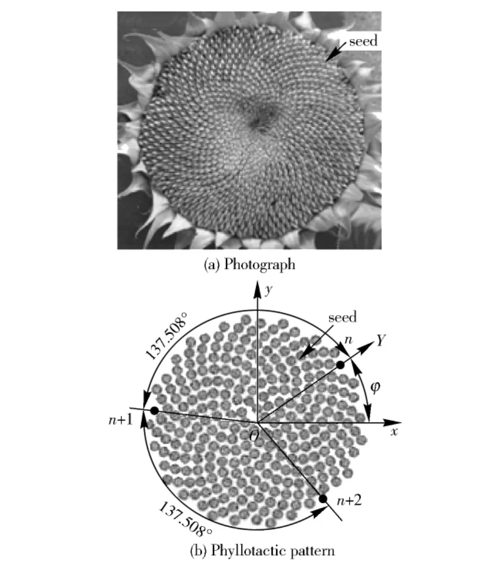
Fig.1 Schematic diagram of sunflower seeds
1.2 Design of Polishing Pad
Figure 2 shows the bionic polishing pad with phyllotactic pattern.The bionic polishing pad is made up of copper foil and tin fixed abrasive blocks.The copper foil is a basic pad with 0.2 mm thickness.The tin fixed abrasive block is made up of tin and diamond grits,The height of the fixed abrasive block is 0.2 mm,the size of diamond grit is 200 nm.The polishing pad diameter isΦ160 mm.

Fig.2 Model of bionic polishing pad with phyllotactic pattern
Different phyllotaxis arrangement can be obtained by changing the diameterDof abrasive block and the phyllotactic coefficientkof polishing pad,as shown in Fig.3.In Fig.3,the arranging density of the tin fixed abrasive blocks increases with the decrease in phyllotactic coefficientk,and the width of line groove becomes smaller.When the region of the tin fixed abrasive blocks relative to the polishing pad increases with the increase in the diameterDof tin fixed abrasive block,the width of line groove also becomes smaller.

Fig.3 Effect of the phyllotactic parameters on the patterns
1.3 Fabrication of Polishing Pad
The polishing pad with phyllotactic pattern can be fabricated by using photolithography technology and composite electroplating technology.The fabricating process of the bionic polishing pad is shown in Fig.4[13].The components of electroplating solution and the electroplating parameters are shown in Tab.1.Before electroplating,the diamond grits and copper foil are pre-processed by the use of alkaline liquid and organic solvents.After electroplating,the polishing pad is taken out from the electroplating solution and washed.Fig.5 shows a fabricated bionic polishing pad with phyllotatic pattern.

Fig.4 Fabrication processes of the polishing pad with phyllotactic pattern

Tab.1 Electroplating solution and parameters
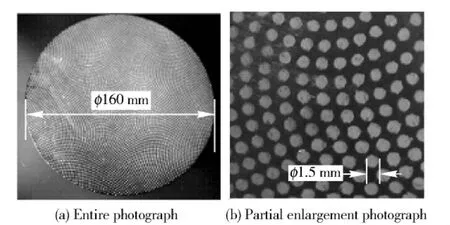
Fig.5 Photograph of bionic polishing pad with phyllotactic pattern
2 Experimental Set-up and Procedure
The experiment was carried out on a lap-polisher.The lap-polisher and its driving principle are shown in Fig.6.Its movement mechanism is mainly composed of tie bar,ring gear and planetary gear which are fixed on the lap-polishing platen and so on.The lap-polisher has two degrees of freedom and two motors.The motors are used to drive the tie bar shaft and the ring gear shaft for polishing movement by a timing-belt,respectively,and at the same time,the planetary gear obtains a rotational movement,which can make the abrasive grits on the lap-polishing platen surface form a complex lapping and polishing cutting trajectory.In the polishing of wafer,the wafer surface is pressed to the lappolishing platen surface for mutual friction and cutting.The polishing load is exerted by a cylinder,and a polishing cantact pressure can be obtained by changing the pressure of compressed air which is input into the cylinder.
In polishing experiment,the diameter of polishing pad for polishing JGS-2 wafer isΦ160 mm,the size of polished wafer isΦ76 mm,the characteristic parameters of wafer are shown in Tab.2,and the flow rate of polishing slurry is 56 mL/min.In order to decrease the effects of the movement parameters of lap-polisher on the uniformity of material removal rate on the wafer surface,the rotation speeds of the ring gear and the tie bar shaft are selected as 133 rpm and 2.2 rpm,respectively[14].The polishing time is 120 min.Before polishing experiment,the wafer surface is lapped,its suface roughnessRais 0.8 μm,and its flatness error is smaller than 0.33 μm.The profile of polished wafer surface was measured by use of an optical flat under the condition of Natrium light with wavelengthλof 0.589 5 μm.The material removal rate was measured by using an electronic balance made by Shanghai Fangrui Instrument Co.LTD,and the material removal thickness on wafer can be calculated.The surface roughness was measured by using Type TR200 contourograph made by TIME Inc.

Fig.6 A lap-polisher for polishing wafer

Tab.2 Characteristic parameters of JGS-2 wafer
3 Results and Discussion
3.1 Surface Profile
Figure 7 shows the influence of the phyllotactic parameters on the surface profiles of polished wafer.It can be seen from Fig.7 that the planarization region of polished wafer is maximal when the phyllotactic coeffiecinetkis betwwen 1.0 and 1.1 and the diameterDof abrasive block isΦ1.6 mm,but the turned-down edge effect of wafer surface is relative large when the diameterDof the abrasive block isΦ1.6 mm.And actually,the planarization region of polished wafer is better forD=1.3~ 1.4 mm.According to Fig.3,when the phyllotactic coeffiecinetkbecomes small and the diameterDof abrasive block becomes large,the line groove of polishing pad also becomes small,the polishing slurry easily gathers in the outside boundary of polishing wafer,which can lead to exacerbate the over-cutting phenomenon in the outside boundary region of polishing wafer.When the phyllotactic coefficientkof polishing pad becomes large and the diameterDof abrasive block becomes small,the total contact region between the tin fixed abrasive blocks and the wafer becomes small,the contact pressure between the polishing pad and the wafer becomes large,and its singularity in the outside region of the wafer is also intensified,so that the removal thickness of material in the outside region of polished wafer increases,and the surface profile of polished wafer becomes poor under the condition of constant polishing load[15].

Fig.7 Influence of phyllotactic parameters on the surface profiles of polished wafer
3.2 Surface Roughness
Figure 8 shows the influence of the phyllotactic parameters on the surface roughnessRaof polished wafer.In Fig.8,it is seen that the surface roughnessRaof polished wafer is minimal when the phyllotactic coefficientkis between 1.0 and 1.1,and the diameterDof the abrasive blocks is betweenD=1.3 mm andΦ1.4 mm.In practical polishing,it can be observed that,when the phyllotactic coefficientkis relative small or the diameterDis relative large,the flow state of polishing slurry is poorer,the polishing wastes(including abrasive,wafer crumbs,tin metal,etc.)reunite easily and sandwich between the abrasive block and wafer surface to cut and brush the polished surface because of smaller width of the line groove,therefore making the scratch marks of the polished surface increase.When the phyllotactic coefficientkis relative large or the diameterDis relative small,the cutting depth of an abrasive will become large since the contact region between the polishing pad and wafer becomes small,which makes the contact pressure between the abrasive block and the wafer surface becomes large under the condition of constant polishing load[15].
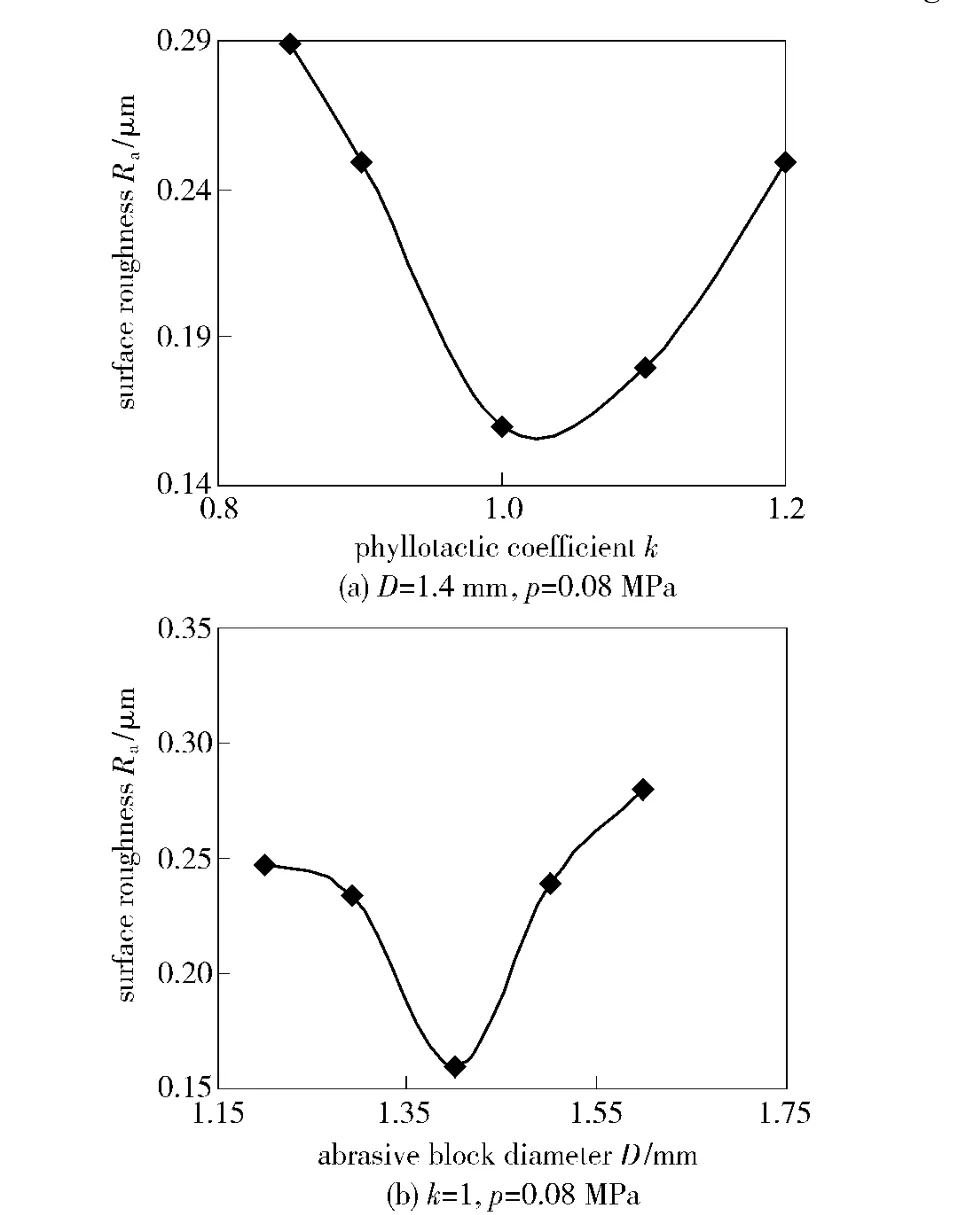
Fig.8 Influence of the phyllotactic parameters on surface roughness of polished wafer
3.3 Material Removal Rate
Figure 9 shows the influence of the phyllotactic parameters on the material removal rate of polished wafer surface.From Fig.9,it can be seen that the material removal rate decreases with the increase in the phyllotactic coeffiecinetkof polishing pad,and increases with the increasing of the diameterDof the abrasive block of the polishing pad.As shown in Fig.3,when the phyllotactic coeffiecinetkof polishing pad deceases and the diameterDof abrasive block increases,the contact ratio of abrasive block to wafer surface also increases,so the total number of the abrasives which can enter into polishing region increases,which makes the mechanical action of polishing processes become large.

Fig.9 Influence of phyllotactic parameters on material removal rate of polished wafer surface
4 Conclusions
A kind of polishing pad with phyllotactic pattern was designed based on the phyllotaxis theory of biology,and the polishing pads with the tin fixed abrasive blocks were fabricated with the use of electroplating technology and photolithography technology.Lastly,the polishing experiments for the wafer were achieved by use of the polishing pad with the tin fixed abrasive blocks which is arranged with phyllotactic pattern.The conclusions can be drown as follows.
1)The polishing pads with phyllotactic pattern can be designed based on the phyllotaxis theory,and fabricated by electroplating and photolithography technologies.The change of phyllotactic parameter has an influence on the arrangement density of the tin fixed abrasive blocks.The increase in the diameterDof tin fixed abrasive block and the decrease in its phyllotactic coefficientkcan increase the contact region between the polishing pad and polishing wafer surface,but the line groove of the polishing pad may become narrow to weaken the flowing state of polishing slurry.
2)When the diameterDof tin alloy block and the phyllotactic coefficientkare 1.3 mm~1.4 mm and 1.0 ~1.1,respectively,the surface roughness and flatness profile of polished wafer can be improved.But the material removal rate increases with the increase in the diameterDof tin fixed abrasive block of polishing pad and with the decrease in the phyllotactic coefficientkof polishing pad.
[1]SHI F G,ZHAO B.Modeling of chemical-mechanical polishing with soft pads[J].Applied Physics A:Materials Science& Processing,1998,67(2):249-252.
[2]Chiou Y C,Lee R T,Yau C L.A novel method of composite electroplating on lap in lapping process[J].International Journal of Machine Tools& Manufacture,2007,47:361-367.
[3]Choi J Y,Jeong H D.A study on polishing of molds using hydrophilic fixed abrasive pad[J].International Journal of Machine Tools& Manufacture,2004,44:1163-1169.
[4]Martin Kulawski.Advanced CMP processes for special substrates and for device manufacturing in MEMS applications[M].Espoo:VTT Publications 611.2006:60 -80.
[5]Lee S,Hwang E.SMART pad fabrication for CMP[R].LMA Research Reports,2002:100 -104.
[6]David B James.Fixed abrasive polishing system for the manufacture of semiconductor devices,memory disks and the like:US,6069080[P].2000-05-30.
[7]Kim H Y.Self-conditioning fixed abrasive pad in CMP[J].Journal of the Electrochemical Society,2004,151(12):858-862.
[8]SU Jian-xiu,KANG Ren-ke,GUO Dong-ming,et al.Study on fixed-abrasive chemical-mechanical polishing technology of wafer in integrate circuit manufacturing[J].Lubrication Engineering,2005,169(5):1 -8(in Chinese)
[9]SHEN Liang-jian.Study on the fixed abrasive polishing pad for micro-electronics manufacturing[D].Nanjing:NanjingUniversityofAeronauticsand Astronautics,2008.(in Chinese)
[10]Neumann P,Carpendale S,Agarawala A.Phyllotrees:phyllotactic patterns for tree layout[M].Eurographics:IEEE-VGTC Symposium on Visualization,2006.
[11]Vogel H.A better way to construct the sunflower head[J].Mathematical Biosciences,1979,44:3 -4,179 -189.
[12]Douady S,Couder Y.Phyllotaxis as a dynamical self organizing process partⅠ:the spiral modes resulting from time-periodic iterations[J].J Theor Biol,1996,178:255-274.
[13]LU Yu-shan,KOU Zhi-hui,WANG Jun.Design and fabrication on the electroplating polishing pad with phyllotactic pattern[J].Advanced Materials Research,2012:472-475,2568 -2573.
[14]WANG Jun,LU Yu-shan.Design and analysis on kinematics of the lap-polisher with planet movement for optical fiber end-face[J].Int J Adv Manuf Technol,2010,50:651-658.
[15]WANG Jun,XING Xue-ling,LU Yu-shan.Contact pressure distribution of chemical mechanical polishing based on bionic polishing pad[C]∥Proceedings of SPIE,International Society for Optical Engineering,2011,7997:2u1-2u7.
猜你喜欢
杂志排行

Defence Technology的其它文章
- An Approximate Calculation Method for Lateral Trajectory Correction
- Lift Enhancement and Oscillatory Suppression of Vortex-induced Vibration in Shear Flow by Loentz Force
- A Study on Criteria for Barrel Lifetime
- Research on Microcrack Extension Mechanism of SiCp/Al in the Machining Process
- Molecular Dynamic Simulation for HMX/NTO Supramolecular Explosive
- Monitoring Method for the Electrical Properties of Piezoelectric Transducer