一种采用CDS电路的高精度CMOS温度传感器*
2012-06-10孔谋夫
孔谋夫
(电子科技大学电子薄膜与集成器件国家重点实验室,成都610054)
A temperature sensor is an essential unit in many integrated circuits(ICs),especially in power devices and power or thermal management chips.A large variety of temperature sensors have been developed to match these technical requirements.In the last couple of years CMOS temperature sensors have become increasingly popular because of rapid steady growth of IC industry and the necessity of effective thermal management in the power hungry and management circuits[1].The basic and the most popular temperature sensor is the bipolar junction transistor(BJT)which can be used as a temperature sensor when operated in a diode configuration,and can be realized in most of the CMOS processes[2-5].
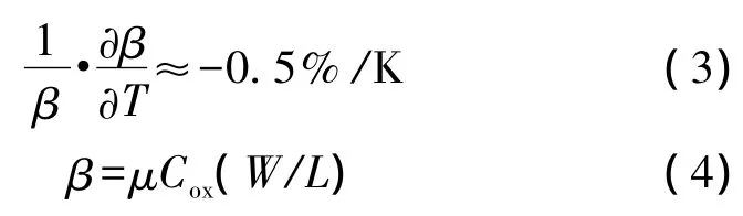
In the BJT solution,the base-emitter junction of a substrate PNP transistor is usually used as a conventional thermal diode whose collector is connected to the ground in CMOS processes.The base-emitter voltage Vbeof a bipolar transistor decreases almost linearly with temperature. The temperature coefficient is approximately 2 mV/℃[1].Figure 1 shows the conventional structure of integrated CMOS temperature sensors by using PNP transistors as thermal diodes,and the output voltage Voutcan be calculated as follows:
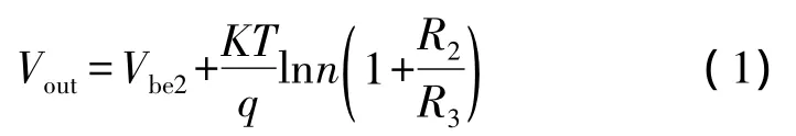
Where K is Boltzmann’s constant,T is the absolute temperature in Kelvin,q is the elementary electric charge and n is the emitter current density ratio of Q2and Q1.Obviously,there isa linearrelationship between the obtained voltage Voutand the temperature T by choosing appropriate values of n,R2and R3.Howev-er,in this structure,the offset voltage of amplifier A will cause large errors.
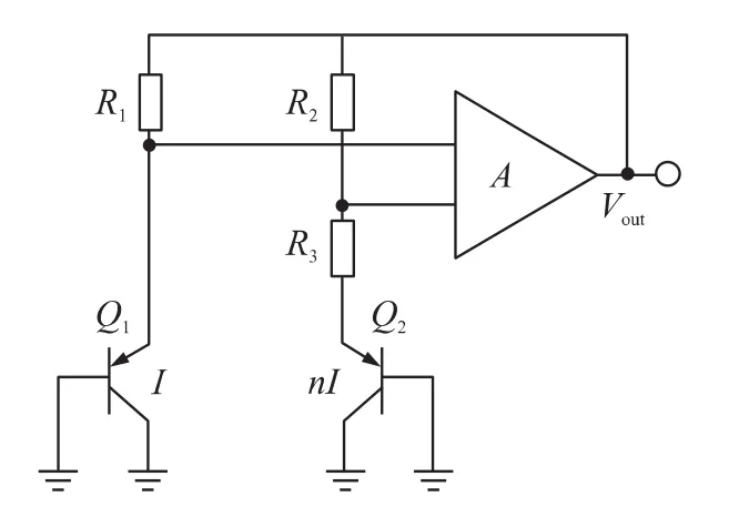
Fig.1 Conventional Structure of Integrated CMOS Temperature Sensor
As for temperature sensors,the quality of the lateral bipolar transistor depends heavily.In many processes,especially when no attention has been paid to optimizethis device,the currentgain ofthis transistor is very low(<5)and the leakage current toward the substrate(via the parasitic vertical bipolar)is difficult to control;and for the vertical bipolar substrate transistor in the temperature sensors,the quality of this transistor is comparable to transistors in standard bipolar processes.However the main problem is the lack of a free collector terminal,which is inherently connected to the substrate[6-7].
Recent researches showed that it is possible to make temperature sensors using CMOS transistors operating in weak inversion[8-10].And this paper presents a novel in-chip temperature sensor solution with CMOS transistors.A correlated double sampling(CDS)circuit is designed which can eliminate kTC noise and reduce 1/f noise of the sensor.
1 Circuit Design and analysys
1.1 Nine-Transistor Temperature Sensor
The new nine-transistor temperature sensor is shown,exclusive of the CDS circuit,is shown in Fig.2.Mp1~Mp4 and Mn1~Mn5 constitute a nine-transistor temperature sensor,and the four P channel MOS transistors Mp1~Mp4 constitute a cascade current mirror.The current of N channel MOS transistors Mn1 is mirrored to transistors Mn2 and Mn3.This temperature sensor utilizes the temperature dependence of two parameters of the MOS transistor,namely,the threshold voltage VTHand the gain factor β.These dependencies are on the order of[8-9]

Fig.2 Schematic of Proposed Temperature Sensor
Whereμ is carrier mobility(for PMOS the carrier is hole μ = μpand for NMOS the carrier is electron μ =μn),Coxis the gate oxide capacitance per unit area,W is the transistor width,and L denotes the transistor effective channel length.
The output voltage of node V1and V2can be expressed as follows:

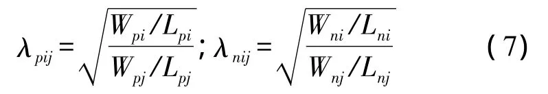
Where λpijand λnijare determined by the ratio between the gate sizes of the transistor pair of PMOS and NMOS,respectively.
The voltage V1controls the gate of the transistor Mn5 yielding a drain current[12-13]of
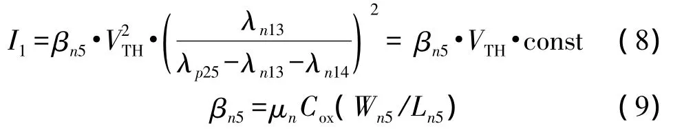
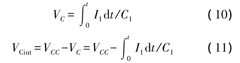
The characteristic of equations(8)and(9)show that the output current is proportional to the temperature.The I1current of the nine-MOS-transistor analogue sensor discharges the capacitor C1.So the voltage drop VCon the capacitor C1and the voltage of node VCintyield by I1are follows,respectively:
Then,the voltage single is send to the CDS circuit.
1.2 CDS Circuit
CDS is a widespread noise reduction method for discrete-time output signals[11].Schematic view of CDS is shown in Fig.3[14].At time T1,by activating the switch S1,the first sample(sample1)is taken and the sampled signal is stored on the sampling capacitor CS1.And,at time T2,switch S2is activated and a new signal(sample2)is sampled and stored on capacitor CS2.
Sample1 retains information about 1/f noise and kTC noise.Sample2 contains both the available signal,and 1/f noise,kTC noise.Then the differential amplifier subtracts these two sampled signals eliminating common noise components from the available information signal.
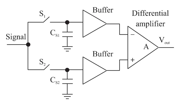
Fig.3 Schematic View of CDS
The proposed CDS circuit is shown in Fig.2.The NMOS transistor Msn and the PMOS Msp constitute a CMOS transmission gate,CS2is a CDS capacitor,NMOS Mc is a clamp transistor and PMOS Mp5 and Mp6 constitute a common-source amplifier.The CDS function is described below.
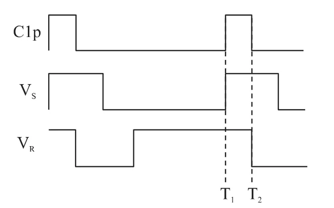
Fig.4 Timing of CDS
Fig.4 shows the timing of CDS circuit.At time T1,the sample clock VSand the clamping clock Clp are high and the clamp transistor Mc is ON.The first sampled voltage signal is charged on the CDS capacitor CS2and the voltages of node V3and V4at time T1are:

where Vnoiseis sum of 1/f noise and kTC noise of the circuit.
At time T2the clamp device Mc is turnnig OFF before the internal integration capacitor C1is reset.Then the second sampled voltage signal of node V3becomes:

since the charges on the ac coupling capacitor C2are the same at time T1and T2.From(12)~(14),we have:

Thus,the output signal of node V4after the CDS is:

Then the voltage signal V2(T2)is sent to the commonsource amplifier.
2 Simulation and analysys
The simulation results in 0.6 μm CMOS process of node VCintand Voutare shown in Fig.5 and Fig.6,respectively.The temperature is from 0℃ to 160℃ with delta=20℃.
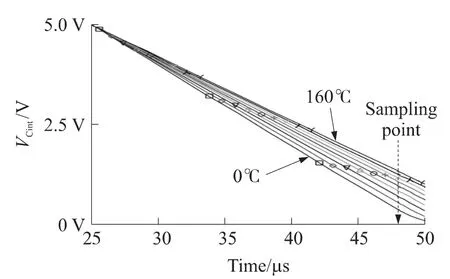
Fig.5 Simulation Result of node VCint
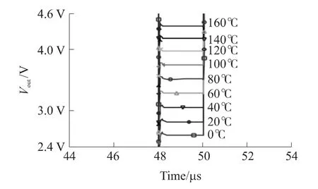
Fig.6 Simulation Result of node Vout
Fig.7 shows the characteristics of output voltage Voutwith temperature T from simulation results with temperature from 0℃ to 160℃,delta=20℃.Formula(17)is a fitting function of output voltage Voutwith temperature T.And it indicates that there is a good linear relationship between Voutand the temperature T in the range of 0℃to 160℃.
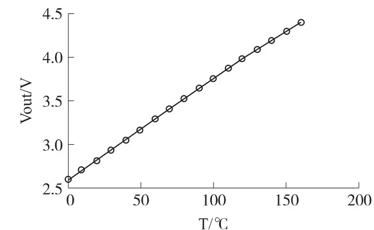
Fig.7 Characteristics of Voutwith Temperature
Table 1 shows the briefview of the proposed temperature sensor,and it has a wide temperature range,a high temperature coefficient and low power consumption.Another advantage of the sensor is it can be fabricated in CMOS process.
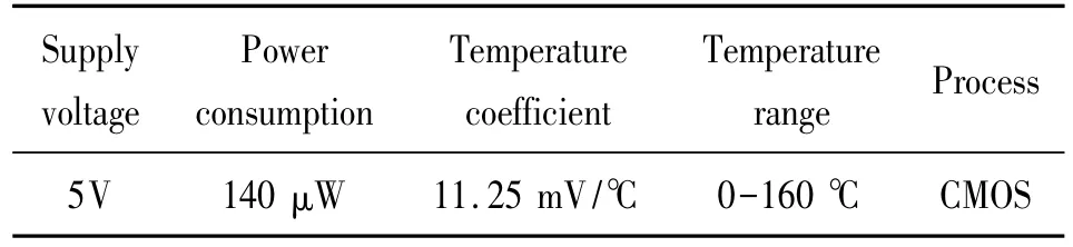
Table 1 Performance of the sensor
3 Conclusions
A novel accurate CMOS temperature is proposed in this paper.The CMOS temperature sensor consisted mainly of 2 parts:a nine-MOS-transistor temperature sensor and a CDS circuit.The MOS transistors can overcome bipolar transistor’s shortcomings and the CDS circuit can eliminate kTC noise and reduce 1/f noise.
The CMOS temperature sensor is analyzed and verified by simulation.The simulation results show the sensor has a high temperature coefficient and the output voltage has a good linear relationship with the temperature.The proposed temperature sensor can be fabricated in standard CMOS process without using PNP bipolar transistors.
[1]Florin Udrea,Sumita Santra,Julian W Gardner.CMOS Temperature Sensors-Concepts,State-of-the-Art and Prospects[C]//Semiconductor Conference,CAS 2008.International Issue Date:13-15 Oct.2008:31-40.
[2]Omar Fathy,Ahmed Abdallah,Amr Wassal,et al.Counter Based CMOS Temperature Sensor for Low Frequency Applications[C]//Thermal Issues in Emerging Technologies Theory and Applications(ThETA),2010 3rd International Conference,2010:103-109.
[3]André L Aita,Kofi A A Makinwa.Low-Power Operation of a Precision CMOS Temperature Sensor Based on Substrate PNPs[J].Sensors,2007:856-859.
[4]林摇荣,蔡摇敏,黄伟朝,等.新型低功耗CMOS片上温度传感器设计[J].传感技术学报,2011,24(7):981-985.
[5]Bakker A,Huijsing J H.Micropower CMOS Temperaturesensor with Digital Output[J].IEEE J Solid-State Circuits,1996,31(7):933.
[6]Pertijs M,Niederkorn A,Ma X,et al.A CMOS Temperature Sensor with a 3σ in Accuracy of±0.5 ℃ from -50 ℃ to 120 ℃.IEEE International Solid-State Circuits Conference(ISSCC),2003:1:200.
[7]Bianchi R A,Karam J M,Courtois B,et al.CMOS-Compatible Temperature Sensor with Digital output for Wide Temperature Range Applications.Microelectronics Journal,2000:31:803.
[8]Masahiro Sasaki,Makoto Ikeda.A Temperature Sensor with an Inaccuracy of-1=+0.8 C using 90-nm 1-V CMOS for Online Thermal Monitoring of VLSI Circuits[J]. Semiconductor Manufacturing,IEEE Transactions,2008,21(2):201-208.
[9]Vladimir SzCkely,Cs MBrta,Zs Kohki,et al.CMOS Sensors for on-Line Thermal Monitoring of VLSI Circuits[J].Very Large Scale Integration(VLSI)Systems,IEEE Transactions,1997,5(3):270-276.
[10]Chen Zhao,Jun He,Sheng-Huang Lee,et al.A Linear Differential Output of Threshold-Based CMOS Temperature Sensor with Enhanced Signal Range[C]//Circuits and Systems(MWSCAS),2010 53rd IEEE International Midwest Symposium,2010:316-319.
[11]Chen Xu,Shen Chao,Mansun Chan.A New Correlated Double Sampling(CDS)Technique for Low Voltage Design Environment in Advanced CMOS Technology[J].Solid-State Circuits Conference,ESSCIRC Proceedings of the 28th European,2002,9:117-120.
[12]曹新亮,余宁梅,卫秦啸.集成CMOS温度传感器设计、实现和测试[J].传感技术学报,2010,23(1):38-42.
[13]Vladimir SzCkely,Cs MBrta,Zs Kohki,et al.CMOS Sensors for on-Line Thermal Monitoring of VLSI Circuits[J].Very Large Scale Integration(VLSI)Systems,1997,5(3):270-276.
[14]Rankov A,Rodriguez-Villegas E,Lee M J.A Novel Correlated Double Sampling Poly-Si Circuit for Readout Systems in Large Area X-Ray Sensors[J].Circuits and Systems,2005.ISCAS 2005.IEEE International Symposium,2005,1:728-731.