Low-damage interface enhancement-mode AlN/GaN high electron mobility transistors with 41.6%PAE at 30 GHz
2023-12-02SiYuLiu刘思雨JieJieZhu祝杰杰JingShuGuo郭静姝KaiCheng程凯MinHanMi宓珉瀚LingJieQin秦灵洁BoWenZhang张博文MinTang唐旻andXiaoHuaMa马晓华
Si-Yu Liu(刘思雨), Jie-Jie Zhu(祝杰杰),†, Jing-Shu Guo(郭静姝), Kai Cheng(程凯),Min-Han Mi(宓珉瀚), Ling-Jie Qin(秦灵洁), Bo-Wen Zhang(张博文),Min Tang(唐旻), and Xiao-Hua Ma(马晓华),‡
1Key Laboratory of Wide Bandgap Semiconductor Technology,School of Microelectronics,Xidian University,Xi’an 710071,China
2Enkris Semiconductor,Inc.,Suzhou 215123,China
3State Key Discipline Laboratory of Radio Frequency Heterogeneous Interation,Shanghai Jiao Tong University,Shanghai 200240,China
Keywords: GaN,low damage,enhancement mode,power-added efficiency
1.Introduction
With the development of high-voltage switches and highspeed radio-frequency (RF) circuits, GaN semiconductors have been widely used in the field of RF power electronic devices due to their excellent material properties.The highelectron-mobility transistors (HEMTs) fabricated by conventional process are all depletion-mode devices and cannot form logic complementation.Therefore, a negative voltage circuit needs to be designed to turn off the device in circuit design.[1,2]In order to expand the application scope of GaN-based HEMT devices in mobile terminals, research on enhancement-mode(E-mode) GaN-based HEMTs has gradually become a research hotspot.Compared with the current mainstream GaAs technology, GaN technology can provide high efficiency and power density.[3–5]In short,the scaling E-mode devices bring new challenges and opportunities for the fabrication of RF Emode devices.[6–8]
In order to achieve low-power logic complementarity,simplify the circuit structure and reduce the chip size, the conventional E-mode device fabrication process of recessed gate structure and p-GaN structure cannot ensure the fabrication of low-damage RF E-mode devices.[9–11]This is due to the scaled gate length and lateral dimensions making process compatibility problematic.[12–14]Owing to the necessity of high frequency and RF power performance,thin barrier materials with strong polarization are more conducive to fabricating RF E-mode devices.As reported, the AlN/GaN has extremely high two-dimensional electron gas(2DEG)concentration,ultra-thin barrier layer,and a process compatible with InAlN and ScAlN.[15–17]In order to reduce the influence of etching,ion implantation,and other processing methods on the 2DEG channel,we have proposed the remote plasma oxidation(RPO)processing method to fabricate AlN/GaN enhancement mode devices with excellent results.[17]
In terms of the oxidation method, there have been many studies in the literature.For example,the RIE O plasma treatment reported in Refs.[18,19]can also obtain E-mode devices,but the parallel plate in RIE mode will increase the plasma energy and inevitably cause damage to the barrier layer.In Refs.[20,21] oxygen plasma treatment at 800-W power was reported.Oxidation treatment in the full access area is difficult to control the threshold voltage and saturation current of the device during the fabrication of RF devices.
The advantage of RPO treatment is that the threshold voltage can be regulated without affecting the 2DEG channel, so that the device can be enhanced.A series of methods to enhance the device such as recessed gate and F ion implantation will cause some damage to the channel.With the positive drift of the threshold, these damages will gradually increase, bringing more reliability problems to the device.In the metal–insulator–semiconductor (MIS) devices, the interface between the insulating layer and the barrier layer can create problems such as heightened off-state leakage or diminished peak transconductance.Through comprehensive consideration, combining the characteristic of the AlN barrier layer oxidized easily, the RPO method is used to make the lower part of the gate into AlON that can theoretically reduce leakage, increase breakdown, and well control interface damage compared with etching.Almost no impurity particles are generated,which greatly reduces the scattering effect of impurities or defects on the 2DEG of the channel.The RPO technology also has unique advantages in making RF E-mode devices.Comparing with the conventional scaling gate and recessed gate device fabrication, the aspect ratio will cause the etching rate to drop sharply, the unstable etching rate will lead to a low yield, and the inevitable lateral etching will reduce the fidelity of the lines.The RPO approach ignores aspect ratio and enables small lines with higher fidelity, which is critical for RF device fabrication.
This paper reports the RF E-mode AlN/GaN HEMTs fabricated by the RPO treatment, with a contact resistance of 0.29 Ω·mm, a threshold voltage (Vth) of 0.5 V, a maximum current of 1.16 A/mm,and a 46-V breakdown voltage.It has a power density of 1.38 W/mm(0.85 W/mm)and a power added efficiency of 61.9%(41.6%)at 3.6 GHz(30 GHz).
2.Device fabrication
In this work,we used a 3-inch-thick(inch=2.54 cm)SiC substrate epitaxial wafer fabricated by metal-organic chemical vapor deposition.From bottom to the top, the structure materials were SiC substrate, 80-nm AlN nucleation layer,2-µm-thick UID-GaN,2.9-nm-thick ultra-thin AlN barrier, and 2.1-nm-thickin-situSiN.Hall measurement results showed that the carrier concentration at room temperature is 1.09×1013cm-2, the mobility is 789 cm2/V·s,and the sheet resistance is 737.4 Ω/sq.The ohmic contact between the source electrode and drain electrode was Ti/Al/Ni/Au=20/160/55/45 nm from bottom to top, and an ohmic contact resistance formed after rapid thermal annealing at 860◦C in N2for 60 s was 0.29 Ω·mm.The passivation layer was grown by plasma-enhanced chemical vapor deposition of 60-nm-thick SiN, and then the sheet resistance was reduced to 320 Ω/sq.Thein-situSiN and PECVD-SiN under the gate were removed with CF4/O2mixed plasma etching by inductively coupled plasma.Afterwards,it was determined through many experiments that the AlN region under the gate was thermally oxidized at 300◦C for 2 min by RPO treatment.After that,450-nm-thick Ni/Au=50/400-nm metal was evaporated and used as a T-shaped gate.The schematic cross-section and HAADF-SEM of E-mode AlN/GaN HEMTs are shown in Fig.1(a).
The Al 2p core level spectra are shown in Fig.1(b).For D-mode devices, to avoid the influence of air oxidation, Ar ions were used to etch the sample surface for 1 min before the XPS test.The Al 2p peaks consisted of two components corresponding to the Al–N bond and the Al–O bond.After the RPO treatment, the intensity of the Al–O peak was elevated,indicating that the treatment of AlN produces Al oxides on the surface.By calculating the peak area after fitting,the content of Al–O in AlON accounted for about 82.6%.
As shown in Fig.2(a),we extracted the transfer characteristics of D-mode device and E-mode device on the same wafer with gate lengthLG=0.12µm and source–drain lengthLSD=1.5µm atVD=6 V bias.The off-state leakage of the D-mode AlN/GaN HEMT was about 2.8×10⁻⁷A/mm,the saturation current was 1.74 A/mm,and theIon/Ioffratio was 6×10⁶.For the E-mode AlN/GaN HEMTs treated with RPO for 2 min,the maximum drain current was 1.16 A/mm,the off-state leakage was concentrated in the order of 7.8×10⁻⁹A/mm,and a highIon/Ioffratio was 1×10⁸.However, the sub-threshold characteristics of the device were not good enough, which is caused by poor confinement of the high concentration of the two-dimensional electron gas in the AlN/GaN heterojunction.Figure 2(b)shows the transconductance curves and drain current curves of D-mode device and E-mode device in linear coordinates.TheVthwas determined by using the linear extrapolation method.TheVthof D-mode and E-mode devices were-1.3 V and 0.5 V,respectively.
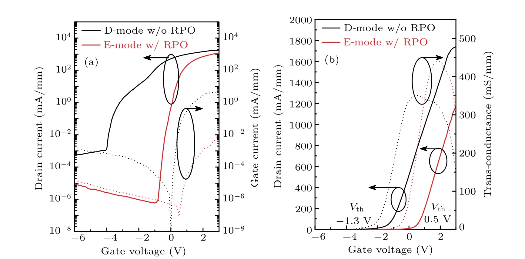
Comparing with the D-mode device, the peak transconductance of the E-mode device increased from 351 mS/mm to 440 mS/mm.The AlN under the gate was processed by RPO to form AlON,and the concentration of 2DEG decreased,thus increasing the mobility of 2DEG.We tested the devices withLG=1 µm andLSD=5 µm.After the RPO treatment, the transconductance of the device increased from 175 mS/mm to 192 mS/mm.The test directly obtained the extrinsic transconductance (gext,peak) of the device, which are related to the intrinsic transconductance value(gint,peak)and the device source resistanceRs,and expressed as
By testing the electrical characteristics of the device in the linear region, theRswas 3.38 Ω·mm for the D-mode device and 3.02 Ω·mm for the E-mode device.Thegint,peakvalues of the two devices were calculated to be 457 mS/mm and 442 mS/mm, respectively.The RPO treatment increased the intrinsic transconductance by about 7%.The intrinsic peak transconductance of GaN-based HEMT devices could be expressed as the product of electron saturation drift velocity and gate capacitanceCg,and expressed as
wherevsatis the channel electron saturation drift velocity,and the gate capacitance takes the value when the gate voltage is 0 V.Substituting the intrinsic transconductance value and gate capacitance into Eq.(2), the channel electron saturation drift velocityvsatcould be obtained.The AlN gate insulating layer increased the saturation drift velocity of channel carriers from 1.11×107cm/s to more than 2.04×107cm/s.Therefore,the peak transconductance of the E-mode device was higher than the D-mode device.
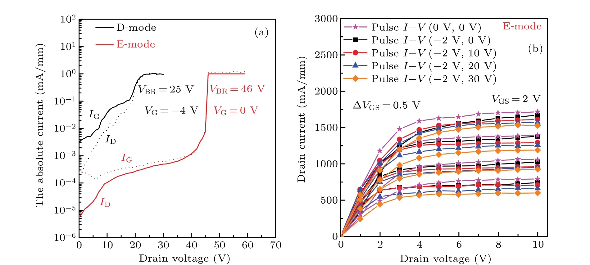
The breakdown characteristics of the devices with a source–drain spacing of 1.5 µm are shown in Fig.3(a).The breakdown voltage was defined where theIDreaches 1 mA/mm.The breakdown voltage increased from 25 V atVG=-4 V(D-mode)to 46 V atVG=0 V(E-mode).Owing to the ultra-thin AlN barrier material, the breakdown mechanism of D-mode devices was gate-breakdown.After several tests, the breakdown mechanism of the E-mode device was transformed into source–drain breakdown, which is because the RPO treatment converts AlN under the gate into AlON,which reduces the gate leakage, and reduces the electric field strength between gate and drain.[17]The higher concentration of 2DEG formed by the AlN/GaN heterojunction led to a further increase in the electric field strength under the condition of high drain voltage.In order to obtain a higher breakdown voltage with the same source–drain spacing, we oxidized the AlN under the gate to reduce the 2DEG concentration.In this way,under the same test conditions,the electric field strength between the gate and the drain could be reduced accordingly.
As shown in Fig.3(b), to evaluate the current collapse,the pulsedI–Vcharacteristics of E-mode AlN/GaN HEMT at different static bias points were extracted.The pulse width and pulse period were 500 ns and 1 ms,respectively.AtVG=0 V andVD=0 V and atVG=-2 V,andVD=30 V,the maximum pulse current was 1.72 A/mm, 1.53 A/mm, respectively.The current collapse amount was 11%.Under the same conditions,we measured a D-mode device collapse rate of 10.9%.The interface state density can be obtained to be 4.62×1010cm-2(without RPO) and 8.2×1010cm-2(with RPO).The good interface state density proved that the RPO process has low damage to the channel.
The device used for CW power testing was a single-finger structure,LSD=1.5 µm,LG=0.12 µm, andWG=100 µm.As shown in Fig.4(a), measurements were made at 3.6 GHz under CW in class AB bias conditions (quiescent drain currentId,q=100 mA/mm,VD=10 V, andVG=0.4 V) for RF power characterization.At the maximum efficiency (power)impedance point, the saturated output power density (Pout)is 1.17 W/mm (1.38 W/mm), the power added efficiency(PAE)reaches 61.9%(55.2%), and the linear gain is 14.0 dB(14.2 dB).
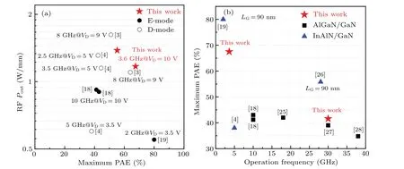
Figure 4(b) shows that measurements that were taken at 30 GHz under CW in class AB bias conditions(quiescent drain currentId,q=100 mA/mm,VD=6 V, andVG=0.2 V).The results showaPoutof 0.85 W/mm, a PAE of 41.6%, and a linear gain of 9.15 dB.These findings indicate the enormous potential of RPO technology in the fabrication of AlN/GaN enhancement-mode RF devices.This demonstrates the great potential of RPO technology in the fabrication of AlN/GaN enhancement-mode RF devices.
As shown in Fig.5(a),the horizontal axis is the maximum PAE of the enhancement mode device,and the vertical axis is the maximum saturated output power.We compared the power levels of D/E-mode devices for AlGaN system with those for InAlN system under low voltage.The E-mode HEMTs with strong-polarization and ultrathin barrier AlN/GaN heterostructures demonstrate that their PAEs are comparable to those with the D-mode AlGaN/GaN (InAlN/GaN) HEMTs for the RF applications.Figure 5(b) shows that the E-mode AlN/GaN HEMTs demonstrate excellent performance for Kaband.This fully proves the practicability of RPO treatment in the AlN/GaN system for 5G-compatible frequency,mobile phone,and base station.
3.Conclusions and perspectives
This paper describes the RF E-mode AlN/GaN HEMTs fabricated by RPO treatment.The device has aVthof 0.5 V,a saturation current of 1.16 A/mm,a 61.9%(41.6%)PAE,and a power density of 1.38 W/mm(0.85 W/mm)in CW power testing at 3.6 GHz(30 GHz).It is worth mentioning that the RPO treatment improves the mobility of the device while reducing the 2DEG density.All results show that the RPO processing method has good applicability for scaling ultrathin barrier Emode AlN/GaN HEMTs for 5G compliable frequency ranging from sub-6 GHz to Ka-band.
Acknowledgements
Project supported by the Fundamental Research Funds for the National Key Research and Development Program,China(Grant No.2020YFB1807403) and the National Natural Science Foundation of China (Grant Nos.62174125, 62188102,and 62131014).
猜你喜欢
杂志排行

Chinese Physics B的其它文章
- Optimal zero-crossing group selection method of the absolute gravimeter based on improved auto-regressive moving average model
- Deterministic remote preparation of multi-qubit equatorial states through dissipative channels
- Direct measurement of nonlocal quantum states without approximation
- Fast and perfect state transfer in superconducting circuit with tunable coupler
- A discrete Boltzmann model with symmetric velocity discretization for compressible flow
- Dynamic modelling and chaos control for a thin plate oscillator using Bubnov–Galerkin integral method