Hexagonal boron phosphide and boron arsenide van der Waals heterostructure as high-efficiency solar cell
2022-09-24YiLi李依DongWei魏东GaofuGuo郭高甫GaoZhao赵高YananTang唐亚楠andXianqiDai戴宪起
Yi Li(李依) Dong Wei(魏东) Gaofu Guo(郭高甫) Gao Zhao(赵高)Yanan Tang(唐亚楠) and Xianqi Dai(戴宪起)
1School of Physics and Electronic Engineering,Zhengzhou Normal University,Zhengzhou 450044,China
2School of Physics,Henan Normal University,Xinxiang 453007,China
Keywords: h-BP,h-BAs,two-dimensional heterostructure,solar cell
1. Introduction
With the development of society,the consumption of fossil fuels and other non-renewable energy sources are increasingly rising up. The scarcity of non-renewable energy sources has led to a great deal of interest in the utilisation of green and renewable energy sources. The collection and use of solar energy is always the focus of research. The conversion of solar cells from optical energy into electrical energy is important for energy production, and searching for new materials and improving the efficiency of photovoltaic conversion become the main research hotspots. Based on existing processing technologies, the solar cell industry has been dominated by traditional silicon-based devices. For this reason, plenty of researchers have turned to improving the power conversion efficiency (PCE) of silicon-based devices, however, their researches are approaching to the theoretical limits.[1]In order to further improve the PCE of solar cells,researchers have investigated other materials as candidates for solar cells,in particular,two-dimensional(2D)excitonic solar cells(XSCs),which have attracted much attention.[2-5]The 2D XSCs consist of two different materials stacked together forming a heterogeneous structure. Owing to the different properties of the two materials,the photo-generated electrons and holes are located on two different materials when illuminated, which enables the electrons and holes to be separated effectively. For heterojunctions,the solar cell is mainly determined by interfacial effect.
Since the successful exfoliation of graphene in 2004,[6]it has caused a boom in the research of 2D materials.The 2D materials are distinguished from bulk due mainly to the presence of only a few atomic layers of thickness in two dimensions, while the scale in the plane is greater than the layer thickness.[7,8]Owing to the effect of quantum confinement, 2D materials exhibit unique properties that distinguish them from bulk and provide potential applications in nanoelectronics,[9]topology,[10]topological insulators,[11]ferroelectricity and antiferroelectricity,[12]optoelectronics,[13,14]photovoltaics,[15]spintronic devices,[16]solar energy harvesting,[17]etc. They also provide a excellent research platform for understanding new types of physics.[8]The preparation of 2D materials is well established by a number of chemical and physical methods like mechanical exfoliation,[18]chemical exfoliation of their bulk structures,[19]chemical vapor deposition(CVD)of thin films,etc.[20]Van der Waals heterostructures (vdWHs) stacked by different 2D materials together vertically, are held together by vdW forces (the same forces that hold the layers together), and this heterostructure allows more combinations than any conventional growth method.[21]The construction of heterostructures brings more opportunities for the applications of 2D materials, such as wearable and biocompatible electronics,[22]photodetectors,[23]photovoltaics,[24-26]and light emitting devices.[27]The design of solar cells using heterojunctions with type-II band alignment is an effective method.
Hexagonal boron phosphide (h-BP) and boron arsenide(h-BAs)are typical 2D materials consisting of group III-V elements,with an atomic structure similar to the graphene.[28,29]The research indicated that bulk boron phosphide(BP)is successfully prepared in the laboratory,[30,31]which means that in the nearest future, h-BP layer is expected to be prepared by mechanical exfoliation. The h-BP layer has excellent carrier mobility (~104cm2·V-1·s-1),[32]comparable to that of graphene (~105cm2·V-1·s-1),[33]and is a direct bandgap semiconductor(~0.89 eV).[28]Cubic BAs is a material with ultra-high thermal conductivity (~2000 W/mK),[34]comparable to diamond and graphite.[35-37]The BAs has been fabricated, and some of their properties have been characterized previously.[38]The cubic BAs and BP were sliced along the (111) face and fully optimized to obtain h-BAs and h-BP monolayers. The electronic and transport properties of h-BP/h-BAs vdwHs have been studied,[39]while their optical properties and PCE have not been discussed.
In this work, the geometry, electronic properties, optical absorption properties,and PCE of h-BP/h-BAs vdwHs are systematically investigated based on the density functional theory calculations. The results indicate that the h-BP/h-BAs vdwHs exhibit a type-II band alignment with large valence band shifts and small conduction band shifts,which is suitable for the design of solar cells. We present models for h-BP/h-BAs vdwHs as solar cells, and calculate the PCE of heterostructures up to 16.51%, which is important for XSCs. This work can increase the understanding of the properties and applications of h-BP/h-BAs vdwHs.
2. Computational methods
First-principles calculations were carried out with the context of density functional theory (DFT) in the generalized gradient approximation with the Perdew-Burke-Ernzerh(PBE)[40]exchange-correlation functional, and the projected augmented wave (PAW)[41]approach with plane wave cutoff energy of 550 eV, as implemented in the Viennaab initiosimulation package (VASP).[42]To correct the bandgap underestimation of PBE, Heyd-Scuseria-Ernzerhof (HSE06)functionals[43]were employed for a more accurate description of the band edges. The zero damping DFT-D3[44]proposed by Grimme was adopted to account for the long range vdW interaction between h-BP layer and h-BAs layer. The atomic positions were fully optimized until the maximum force on each atom was less than 0.01 eV/˚A,and the difference in total energy between two self-consistent cycles reached less than 10-5eV. A vacuum thickness of more than 20 ˚A was used to decouple the periodic images between adjacent monolayers along thezdirection.[45]Akgrid of 11×11×1 was employed in both geometry and electronic properties calculations. The PHONOPY[46]code was used to obtain the phonon dispersion curve through density functional perturbation theory(DFPT).
3. Results and discussion
3.1. Geometry and stability
The geometrical structures of the monolayers are calculated before building the heterostructures. For the intrinsic h-BP and h-BAs monolayers,the optimized lattice constants are 3.21 ˚A and 3.39 ˚A, respectively, which match well with the previous results.[47-50]The 1×1 h-BP and 1×1 h-BAs cells are chosen to form a heterstructure with a lattice constant of 3.39 ˚A,and the lattice mismatch rate is about 5%. With various stacking sequences, the h-BP and h-BAs monolayers can form different heterostructures.As illustrated in Fig.1(b),they are denoted as A,B,C,and D,respectively. In the A conformation,B and P atoms in h-BP layer correspond to B and As atoms in the h-BAs layer,respectively. In the C configuration,the P atom in h-BP layer is located below the B atom in the h-BAs layer,and the B atom is located below the center of the six-membered ring composed of h-BAs layers. The configurations B and D are obtained by rotating the h-BP layer 180°around the vertical axis of the A and C structures,respectively.
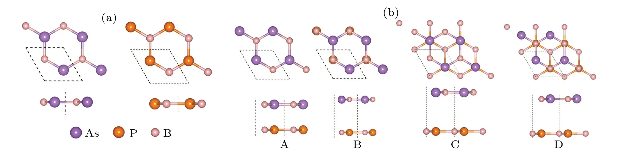
Fig.1. Top and side view of(a)h-BP and h-BAs layers,(b)h-BP/h-BAs vdWHs with various stacking manners.
In order to screen the most stable structures,we calculate the binding energy values of the four heterostructures. The formula for binding energy(Eb)is

whereEh-BP/h-BAs,Eh-BP, andEh-BAsare the total energy of the heterostructure, intrinsic h-BP and h-BAs monolayer,respectively. TheEband layer spacing of the four heterostructures are listed in Table 1. The D-configuration heterostructure has the lowestEb, indicating the most stable structure,thus only the D-configuration is considered in the subsequent study.
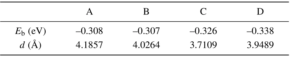
Table 1. Calculated binding energy Eb and distance between h-BP and h-BAs layer d for different stacked patterns.
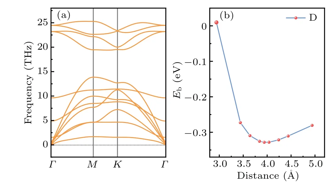
Fig.2. (a)Phonon dispersion curves of h-BP/h-BAs vdWHs,and(b)curve of Eb versus interlayer distance of heterostructure.

Fig.3. Band and structure of(a)h-BP,(b)h-BAs monolayer,and(c)h-BP/h-BAs vdWHs.
For 2D materials, phonon spectroscopy is a reliable way to characterize their kinetic stabilities. The phonon spectrum of the heterstructure is shown in Fig.2(a),and the absence of imaginary frequencies on all high symmetry paths in the Brillouin zone implies the dynamical stability of the structure.The layer spacing significantly affects the structural and electronic properties of the heterostructure. Here, we calculate the evolution ofEbwith layer spacing,indicating that the most stable layer spacing is 3.95 ˚A.
3.2. Electronic properties
Figure 3 shows the band structure of monolayer h-BP,h-BAs,and projected band structure of h-BP/h-BAs vdWHs calculated by the HSE06 method, respectively. The h-BP layer and h-BAs layer are both semiconductors with direct bandgap.The conduction band minimum(CBM)and valence band maximum(VBM)are both located at the high symmetry pointK,with bandgaps being 1.36 eV and 1.14 eV,respectively,which are consistent with previous studies.[28,29]After the formation of the heterostructure, the system still maintains the properties of a direct bandgap semiconductor with a bandgap size of 0.93 eV.Compared with the intrinsic monolayer,the bandgap of the heterostructure is lowered by 0.43 eV and 0.21 eV, respectively, which is mainly caused by the Fermi level alignment. Figure 3(c) shows the projected band structure of h-BP/h-BAs vdWHs, with blue and red representing the contributions of h-BP and h-BAs layer, respectively. To further investigate the electronic properties of h-BP/h-BAs vdWHs,we plot the band decomposed charge densities of heterostructure(Fig.4(a)),which clearly illustrates the type-II band alignment.The CBM is contributed by the h-BP layer and the VBM layer is offered up by the h-BAs layer. When the heterostructure is irradiated by optical light, the valence band electrons of the h-BP layer and h-BAs layer are excited,however,transferred only to the conduction band of h-BP layer, because of the conduction band offset(CBO).
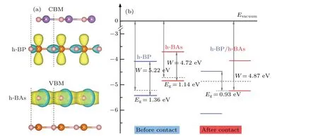
Fig.4. (a)Band decomposed charge densities of band edges with isosurface value of 0.01 e/˚A3,and(b)band alignment of h-BP,h-BAs layers,and h-BP/h-BAs vdWHs.
Meanwhile,during the electron transition from the h-BAs layer to the h-BP layer,except the light-generated holes left in the valence band of the h-BAs layer,the light-generated holes in the valence band of the h-BP layer are transferred to the valence band of the h-BAs layer under the valence band offset(VBO) effect. Therefore, the electron-hole separation redistribution produced by light, which reduces the complexation of electrons and holes, increases the lifetime of the exciton.In h-BP/h-BA vdWHs, a large VBO can contribute to higher efficiency by inhibiting the movement of holes from the h-BP layer(acceptor)to the h-BA layer(donor),which has been applied to both photonics and solar energy conversion.
The work function is critical to the design of devices based on semiconductor heterostructures. As illustrated in Fig.4(b),the work function of h-BP,h-BAs,and h-BP/h-BAs vdWHs are 5.22 eV,4.72 eV,and 4.87 eV,respectively. When h-BP layer contacts the h-BAs layer,electrons will flow from the h-BAs layer to the h-BP layer due to the low work function of h-BAs layer. With the increase of the transferred electrons,the Fermi energy level of the h-BP layer shifts upward. Meanwhile, the Fermi energy level of the h-BAs layer decreases as the number of transferred holes increases, until the Fermi energy levels of the two are aligned. When the equilibrium potential between the h-BP and h-BAs layers is reached,electrons and holes are confined into different layers,which leads to a built-in electric field in the direction from h-BAs to h-BP layer.
Strain can provide a way to probe the change in energy band structure and it is a means of effectively modulating the electronic properties of materials. Here,we provide an insight into the electronic properties of h-BP/h-BAs vdWHs through the biaxial strain. Figure 5(a)shows the top and side views of the h-BP/h-BAs vdWHs under applied compressive strains of 1%-5%, respectively. It can be seen that at a compression strain of 2%, the h-BAs layer in the heterostructure begins to fold and the As atoms are forced to move upwards, while the h-BP/h-BAs vdWHs still retains its semiconductor nature with a type-II band alignment (Fig. 5(b)). As the compressive strain increases further,the As atoms are arched up to an increasing height by the stress and are not in the same plane as the B atoms. At this moment, the h-BP layer remains essentially unchanged and the B atoms and P atoms are still in one plane. When the compression strain increases to 5%, the P atoms start to move upwards under the strain, the P atoms of the h-BP layer become bonded to the B atoms of the h-BAs layer,B-P bond length being 2.108 ˚A,the heterogeneous structure is destroyed and the system behaves metallically as shown in Fig. 5(b). The projected band structures of the h-BP/h-BAs vdWHs under compressive strain are shown in Fig.5(b),
where the heterostructure retains its direct band gap characteristics and maintains the type-II band alignment within the compression strain range from 1%to 4%. As the compressive strain changes, the VBM contributed by h-BAs remains essentially unchanged and the conduction band it contributes to shifts upwards as the strain increases.The h-BP layer,which is the CBM of the dominant h-BP/h-BAs vdWHs, continuously shifts downwards as the compressive strain increases and the band gap of the heterostructure linearly decreases. The blue dashed line and the red dashed line in the figure represent the variations in the conduction band of h-BAs and h-BP layers,respectively.
The top and side views of the h-BP/h-BAs vdWHs under different tensile strains are shown in Fig. 6(a). The h-BP/h-BAs vdWHs remain stable without bond breakage at tensile strains ranging from 1% to 5%, thus indicating that the structure is fully capable of withstanding a 5% tensile strain.In order to accurately describe the h-BP/h-BAs vdWHs band structure and band alignment under tensile strain, we present the projected band structures of the heterostructure at different tensile strains as indicated in Fig.6(b). The conduction band of the h-BP/h-BAs vdWHs shifts upwards with the increase of tensile strain, resulting in an increasing band gap, which can be seen to increase linearly but by a small quantity. The band gap of the heterostructure at 5% tensile strain is 1.10 eV, an increase of 0.17 eV in comparison with that of the intrinsic heterostructure(0.93 eV).The blue and the red dashed lines in the figure refer to the changes in the portion of the conduction band contributed by the h-BAs and h-BP layers,respectively.
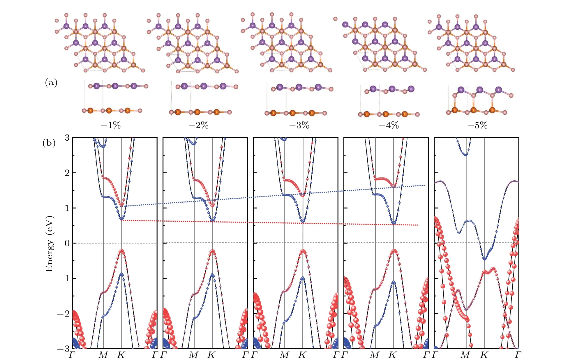
Fig. 5. (a) Top and side view of h-BP/h-BAs vdWHs under different compression strains, and (b) projected band structure of h-BP/h-BAs vdWHs,with red referring to h-BAs layer,and blue representing h-BP layer.
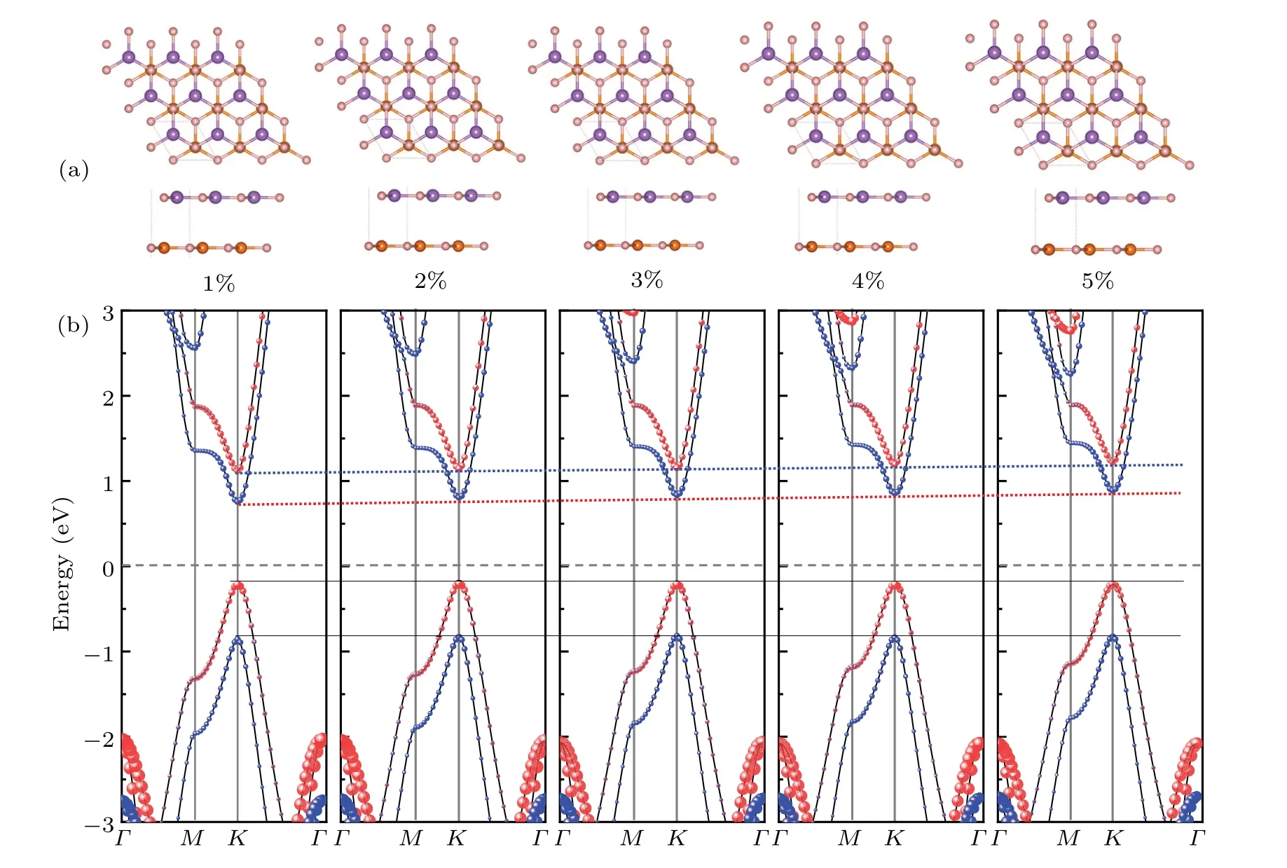
Fig.6. (a)Top and side views of h-BP/h-BAs vdWHs under different tensile strains,and(b)projected band structure of h-BP/h-BAs vdWHs,with red referring to h-BAs layer,and blue representing h-BP layer.
3.3. Optical properties and solar cell
The effective separation between photogenerated electrons and holes in h-BP/h-BAs vdWHs is favorable for the application of photovoltaic materials. Here, we calculate the optical properties and PCE of the h-BP/h-BAs vdWHs.
To explore the optical properties, the frequencydependent dielectric function [ε(ω)] is calculated and obtained, and the light absorption coefficientα(ω) can be obtained from the following equation:[51]
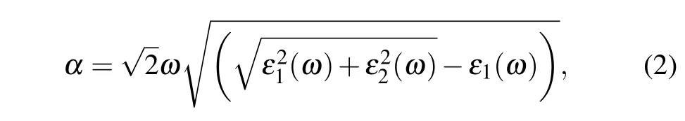
whereε1(ω) andε2(ω) are the real part and the imaginary part of the complex dielectric function,respectively. In Fig.7,the optical absorption coefficients of the intrinsic h-BP,h-BAs layers and heterostructures are calculated, respectively. The results illustrate that the optical absorption peaks of h-BP and h-BAs layers are in the UV region, and also have some optical responses in the visible range and IR range. The absorption peaks of the heterostructure in the visible range are contributed by both h-BP layer and h-BA layer,while the heterostructure has no absorption in the IR range,which may be attributed to the change in the lattice constant after the formation of heterostructure. Compared with the intrinsic layer,the heterostructure maintains good optical absorption properties,and possesses an enhanced visible light absorption range and the optical absorption coefficient of up to 105.
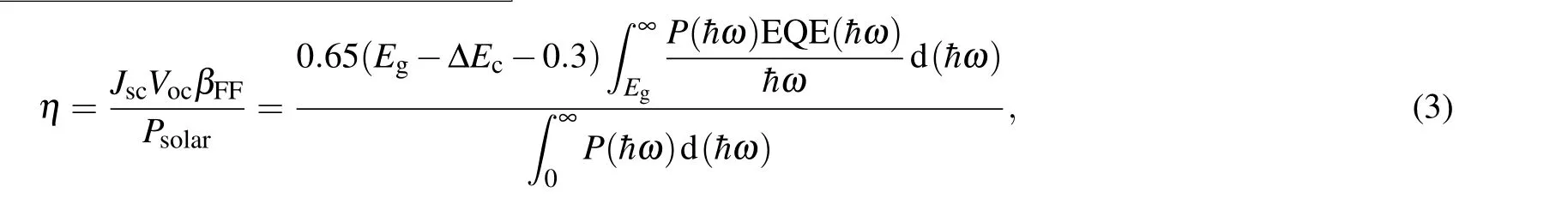

Fig.7. Optical absorption coefficients of h-BP,h-BAs,and h-BP/h-BAs vdWHs at HSE06 level.
The PCE depends greatly on the band alignment between the donor material and the acceptor material. Therefore, it is critically important to select the electron donor and electron acceptor semiconductor materials in 2D XSCs. In view of the excellent optical properties of h-BP/h-BAs vdWHs,we design a solar cell model as depicted in Fig. 8(a). Metal and ITO are used as the electrode materials, and the support substrate is also provided for the heterostructure,with the h-BAs layer serving as the donor material and the h-BP layer as the acceptor material. Once the photons are absorbed, the photogenerated electrons and holes are spatially separated in two different monolayers, creating a photovoltaic voltage and in turn outputting a current to an external circuit.
In the limit of 100%external quantum efficiency(EQE),the upper limit to the PCE is calculated as follows:
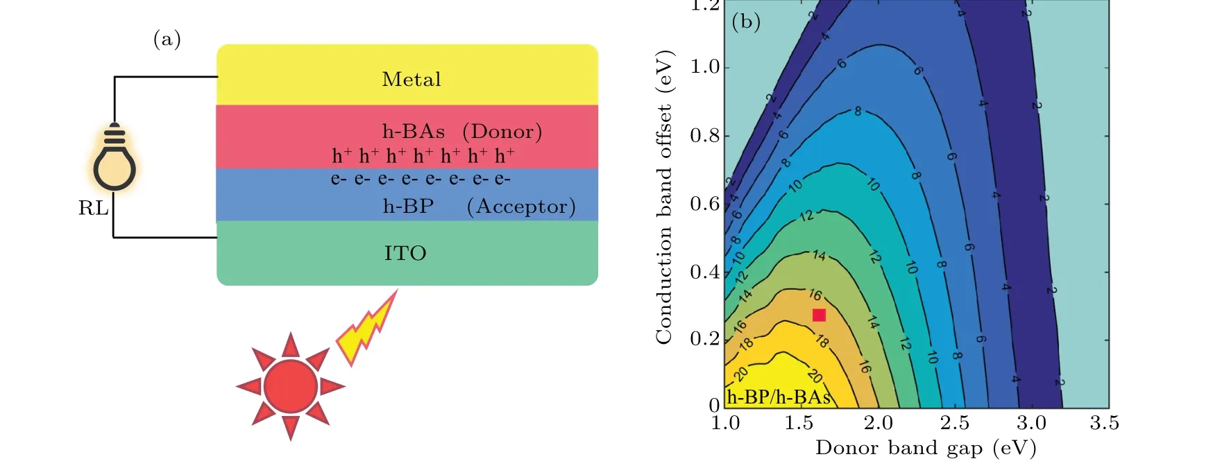
Fig.8.(a)Schematic illustration of thin-film solar cell and internal functional mechanism.RL represents the resistance of the electric apparatus,and(b)calculated power conversion efficiency in heterostructures denoted by red square.
where 0.65 is the band fill factor (βFF);P(¯hω) is taken to be the AM1.5 solar energy flux at the photon energy ¯hω;JSCis the short-circuit current, which is an integral of the solar spectrum;term(Edg-ΔEc-0.3)estimates the maximum opencircuit voltageVoc,Edgbeing the donor bandgap,and ΔEcbeing the CBO.As shown in Fig.8(b),the calculations indicate that the heterogeneous structure has a PCE of up to 16.51%,which is encouraging.
Meanwhile we investigate the effect of biaxial strain on the PCE, and in Table 2 we calculated ΔEc,Edg, and PCE for different tensile-compressive strains.The results show that the PCEs of h-BP/h-BAs vdWHs decrease with tensile strain,but remain in a range of 14.36%-17.12%. This efficiency is competitive with reported efficiencies,for instance,the best certified efficiency of organic solar cells(11.7%),[52]MoSe2/WSe2(14%-16%),[53]phosphorene/MoS2(~21%),[54]MoSe2/BAs(20.08%),[29]and N-GY/MoS2(17.77%).[55]During the experimental preparation of heterojunctions, they are inevitably subjected to tensile or compressive stresses, and our study shows that h-BP/h-BAs vdWHs can still maintain such high PCEs under tensile-compressive strain. Therefore, we infer that the h-BP/h-BAs vdWHs is a potential candidate for the high-efficiency XSCs application.
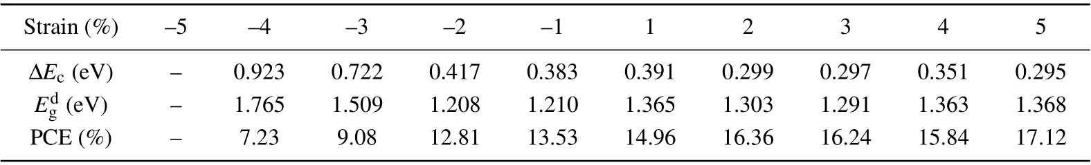
Table 2. Calculated values of ΔEc,Edg,and PCE by biaxial strain regulation.
4. Conclusions
In this work, the electronic and optical properties of h-BP/h-BAs vdWHs are investigated based on first-principles calculations with vdW correction (D3), and the feasibility as an efficient 2D solar cell is proposed. Theoretical calculations indicate that the D heterostructure has the lowest binding energy and has a better kinetic stability. The h-BP/h-BAs vd-WHs exhibit a direct bandgap semiconductor with a bandgap of 0.93 eV,with a type-II band alignment,which enables efficient spatial separation between photo-generated electrons and holes. The h-BP/h-BAs vdWHs can withstand compressive strain up to a limit of 4%compressive strain.For tensile strain,h-BP/h-BAs vdWHs can be regulated in a wide range. From the present study,it can be found that the band gap of h-BP/h-BAs vdWH increases with tensile strain increasing,which can provide some theoretical basis for experiments. In the optical properties, the results show that the heterostructure has a very high absorption coefficient(105cm-1)in the UV-visible range. Meanwhile, the heterostructure has a small CBO, a large VBO,and an PCE of up to 16.51%. These favorable factors highlight the promising future of heterostructures in 2D XSCs.
Acknowledgements
Project supported by the National Natural Science Foundation of China (Grant No. 62074053), the Natural Science Foundation of Henan Province, China (Grant Nos. 202300410237 and 222300420587), the Program for Science & Technology Innovation Talents in Universities of Henan Province,China(Grant No.18HASTIT030),the Henan Overseas Expertise Introduction Center for Discipline Innovation,China(Grant No.CXJD2019005),the High Performance Computing Center of Henan Normal University, China, and the Aid Program for Science and Technology Innovative Research Team of Zhengzhou Normal University,China.
杂志排行
Chinese Physics B的其它文章
- Characterizing entanglement in non-Hermitian chaotic systems via out-of-time ordered correlators
- Steering quantum nonlocalities of quantum dot system suffering from decoherence
- Probabilistic quantum teleportation of shared quantum secret
- Spin–orbit coupling adjusting topological superfluid of mass-imbalanced Fermi gas
- Improvement of a continuous-variable measurement-device-independent quantum key distribution system via quantum scissors
- An overview of quantum error mitigation formulas