A 4H-SiC merged P-I-N Schottky with floating back-to-back diode
2022-02-24WeiZhongChen陈伟中HaiFengQin秦海峰FengXu许峰LiXiangWang王礼祥YiHuang黄义andZhengShengHan韩郑生
Wei-Zhong Chen(陈伟中) Hai-Feng Qin(秦海峰) Feng Xu(许峰)Li-Xiang Wang(王礼祥) Yi Huang(黄义) and Zheng-Sheng Han(韩郑生)
1College of Electronics Engineering,Chongqing University of Posts and Telecommunications,Chongqing 400065,China
2Institute of Microelectronics of Chinese Academy of Sciences,Beijing 100029,China
3Department of Microelectronics,University of Chinese Academy of Sciences,Beijing 100049,China
A novel 4H-SiC merged P–I–N Schottky(MPS)with floating back-to-back diode(FBD),named FBD-MPS,is proposed and investigated by the Sentaurus technology computer-aided design(TCAD)and analytical model. The FBD features a trench oxide and floating P-shield, which is inserted between the P+/N−(PN) junction and Schottky junction to eliminate the shorted anode effect. The FBD is formed by the N-drift/P-shield/N-drift and it separates the PN and Schottky active region independently. The FBD reduces not only the Vturn to suppress the snapback effect but also the Von at bipolar operation. The results show that the snapback can be completely eliminated, and the maximum electric field (Emax) is shifted from the Schottky junction to the FBD in the breakdown state.
Keywords: 4H-SiC,merged P–I–N Schottky(MPS),snapback effect,turnover voltage,floating back-to-back diode(FBD)
1. Introduction
The 4H-SiC power devices have great potential applications for their unique characteristics of high-voltage, highfrequency, and high-temperature.[1–3]The 4H-SiC Schottky barrier diode (SBD) is widely used in high-frequency area due to its unipolar conduction mode. However,the large leakage current limits its breakdown performance and high-voltage application.[4–6]The 4H-SiC P–I–N diode is widely used in high power case due to its bipolar conduction mode.[7–9]However, the poor reverse recovery limits its application in highfrequency area. The 4H-SiC merged P–I–N Schottky (MPS)diode is a promising device by integrating the Schottky and PN junction into one chip,which realizes the superior breakdown performance and fast reverse recover characteristics.[10–14]However, an undesirable snapback effect is induced by the short effect of the Schottky junction at the forward conduction,which can prevent the device from implementing full turn-on,thereby leading to unreliability for the power systems. Many advanced structures have been proposed to solve the snapback in recent years. The L-MPS can suppress the snapback by extending the length of the PN junction, and the anode resistance is increased.[15]The S-MPS can alleviate the snapback turnover voltageVturn,and the width of the PN junction is 1.5 times longer than the thickness of the N-drift.[16]The SP-MPS can not only eliminate the snapback but also reduce the leakage current, and the reverse blocking voltage is increased by the introduced shallow P region.[17]In this paper,a novel MPS with floating back-to-back diode (FBD-MPS) is proposed to eliminate the snapback and reduce the unipolar specific onresistanceRon.
2. Devices structure and equivalent circuit
The cross section schematic and equivalent circuit of conventional MPS(CON-MPS) and the FBD-MPS are shown in Fig.1. For the CON-MPS,it has PN and Schottky junction atthe anode electrode, thus the PIN diodeDPNand Schottky diodeDFSare formed.[18]The N-drift is divided by the equipotential lineW, and theRdrift1andRdrift2are distributed in the equivalent circuit as shown in Fig.1(a). For the FBD-MPS,a transistor N-drift/P-shield/N-drift is designed between the PN and equivalent circuit as shown in Fig.1(b). Additionally,the FBD helps to deplete the N-drift under the Schottky junction,and an extra resistanceis also introduced.

Fig.1. (a)CON-MPS structure and equivalent circuit,and(b)proposed FBD-MPS structure and equivalent circuit,two floating backtoback diodes and R′drift0 introduced.

Table 1. Device parameters of FBD-MPS and CON-MPS.
The key parameters of the proposed FBD-MPS and CONMPS are compared and listed in the Table 1. The widthWDand thicknessTDof the N-drift for each of the two devices are 17.0 µm and 35.0 µm, respectively. The dopingNDof the N-drift and theNAof the P+ anode are 1×1015cm−3and 5×1018cm−3,respectively. For the FBD-MPS,the widthWFP,the thicknessTFP,and the dopingNFPof the P-shield are 1.0µm,4.5µm,and 2×1016cm−3,respectively.
3. Snapback Vturn analytical model
The N-drift for each of the CON-MPS and FBD-MPS is divided into N-drift1 and N-drift2 along the equipotential lineWas indicated in Fig. 1. TheTdrift1for the CON-MPS andfor the FBD-MPS can be expressed by Eqs.(1)and(2),respectively(TP+andTdepleteare the P+anode thickness and the PN junction depletion thickness, respectively.TTOis the trench oxide thickness, andTFBis the floating P-shield thickness for the FBD-MPS).It is noted that theis bigger than
Tdrift1.TheTdrift2for the CON-MPS andfor the FBD-MPS can be expressed by Eqs. (3) and (4) (W1equals 0.5 µm on the assumption that the equipotential lineWin lateral direction is flat within the range ofx>(WO+W1)). It is noted that theis lower thanTdrift2because the equipotential lineWis moved downward by the depletion of the P-shield.

The specific on-resistanceRonof the CON-MPS is the sum of theRdrift1andRdrift2, and theof the FBD-MPS is the sum of theand. The effective thickness of the N-driftTsumfor the CON-MPS andfor the FBD-MPS can be expressed by Eqs.(5)and(6),because the current density through the Schottky contact is(WO+WS)/(WS−Wdeplete)times the current density through the cathode contact as a result of current continuity.It is noted that theTsumis bigger thanTheWdepleteis the PN junction depletion width, which can be expressed by Eq.(7)[19]
The voltage drop across Schottky junctionVFSfor the CONMPS andfor the FBD-MPS can be expressed by Eqs.(8)and(9)(JFCis the cell current density,andφBis the Schottky barrier height).

The voltage drop acrossRdrift2equals (Vturn−VFS)×Tdrift2/Tsum, thus the snapbackVturnfor the CON-MPS andfor the FBD-MPS can be expressed by Eqs.(10)and(11),(VPNis built-in potential of the PN junction). It is noted thatis lower thanVturn.

4. Results and discussion
Figure 2 shows the electron and potential distribution in lateral direction alongy= 34.2 µm for the CON-MPS and FBD-MPS. The trench oxide and floating P-shield is introduced between the PN junction and the Schottky junction, thus the electrons will accumulate under the P+ anode due to the potential barrier of the P-shield as illustrated in Fig. 1(b). Therefore, the electron concentration distribution aty=34.2 µm is extracted to illustrate the accumulation effect, and the potential is explored to reveal the barrier effect.In Fig. 2(a), the electron density of the FBD-MPS is two orders of magnitude higher than that of the CON-MPS at the sameVA=1.5 V and 2.5 V of the unipolar mode, and it is almost the same when the devices operate in the bipolar mode at theVA=3.1 V.The variations of FBD-caused potential barrier with width atVA=1.5 V and 2.5 V of the FBD-MPS are shown in Fig.2(b).

Fig.2. Influences of width on(a)electronic density and(b)potential distribution for the devices at y=34.2µm(WO:WS=15:2).
Figure 3 shows the forwardI–Vcharacteristics of the CON-MPS and proposed FBD-MPS. The snapback is observed for the device due to the short effect of the Schottky anode. The turnover voltageVturnand the extent of snapback ΔVSBincrease withtSchottky junctionWSincreasing.More importantly, the unipolar specific on-resistanceRonof the FBD-MPS is much higher than that of the CON-MPS,which is because the FBD can deplete the N-drift under the Schottky junction,and the extra resistanceis introduced into the equivalent circuit.
Figure 4 demonstrates the influence of theWSandWOon theVturn. TheTsumdecreases withWSincreasing according to Eq.(5). Therefore, theVturnincreases withWSincreasing according to Eq. (10). TheTdrift2decreases withWOincreasing according to Eq.(3),and theTsumandVFSincrease withWOincreasing according to Eqs.(5)and(8). Therefore,theVturndecreases withWOincreasing according to Eq.(10). The simulations and analytical model results are illustrated and compared together as shown in Figs.4(a)and 4(b). Theof the proposed FBD-MPS is much lower than that of the CON-MPS,which is because theandincrease by the FBD.

Fig.3. Forward I–V characteristics of CON-MPS and FBD-MPS,with Vturn denoting turnover voltage,ΔVSB=Vturn −VH,and Ron representing specificon resistance).
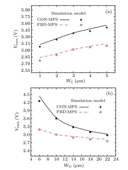
Fig. 4. Variations of Vturn with (a) width WS and (b) width WO of Schottky junction and PN junction,with closed symbols denoting results from analytical model and solid line representing simulation results.
Figure 5 demonstrates the influence ofTDandNDonVturn,ΔVSB,Von,andBV.ForVturn,Tdrift2,andTsumincrease withTDincreasing according to Eqs. (3) and (5), thusVturnincreases withTDincreasing according to Eq. (10). Additionally,Vturngradually increases withNDincreasing according to Eqs. (7)and (10) due to the increase ofWdeplete. The simulations and results from the analytical model are illustrated and compared together as shown in Figs.5(a)and 5(b). For ΔVSB,the snapback is completely suppressed for the FBD-MPS whenTDis shorter than 42.0 µm as indicated in Fig. 5(a). The snapback is also completely eliminated whenNDchanges from 5×1014cm−3to 3×1015cm−3as indicated in Fig.5(b).Additionally,Vonincreases withTDincreasing as shown in Fig.5(a),andBVdecreases withNDincreasing as shown in Fig.5(b)for the devices.
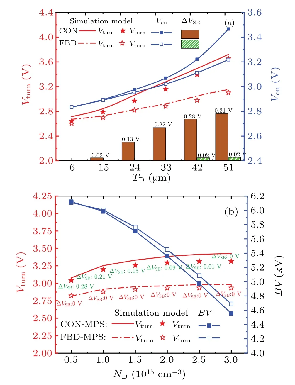
Fig.5. (a)Variations of Vturn and Von with thickness TD in N-drift region for CON and FBD and(b)variations of Vturn and BV with doping concentration ND. (Von is the forward voltage at the current density of 100 A/cm2,and BV is breakdown voltage at leakage current of 10−4 A/cm2).
Figure 6 demonstrates the variations ofandBVwithTFB(see Fig. 6(a)) and withNFB(see Fig. 6(b)) for the proposed FBD-MPS. Forincreases anddecreases withTFBincreasing according to Eqs.(2)and(4), respectively. Thusincreases with the augment ofTFBaccording to Eq.(11). The simulations and results from the analytical model are illustrated and compared together as shown in Fig.6(a). Theis almost the same whenNFBincreases from 5.0×1015cm−3to 3.0×1016cm−3in Fig. 6(b), which is because theWdepleteanddo not depend on theNFBaccording to Eqs. (7) and (6). For ΔVSB, the snapback can be completely suppressed whenTFBis higher than 4.0 µm in Fig.6(a),and the snapback is also completely eliminated whenNFBchanges from 5×1015cm−3to 3×1016cm−3in Fig.6(b).The value ofBVreaches the maximum atTFB=4.0 µm in Fig.6(a)and atNFB=1.5×1016cm−3in Fig.6(b).

Fig. 6. Variations of and BV with (a) TFB and (b) NFB of FBD(WO:WS=15:2).
Figure 7 shows the lateral electric field distributions aty=34.5µm for the devices. The maximum electric fieldEmaxfor the FBD-MPS is shifted from the Schottky junction to the FBD. However, the avalanche breakdownBVfor the CONMPS and FBD-MPS are both 6000 V as shown in the inset.

Fig.7. Curves of Emax and BV versus width for FBD-MPS and conventional CON-MPS at y=34.5µm(WO:WS=15:2).
Figure 8 displays the reverse recovery characteristics of the devices. The reverse recovery timetrris 2.7×10⁻⁸s forthe CON-MPS and FBD-MPS. TheQrrof FBD-MPS is bigger than that of the CON-MPS because more holes are injected at the forward conduction, and it decreases with theenhancement ofWSfor each of the two devices. The values of softness factorSare bigger than 1 and gradually increase with the rise of theWS,thus the soft reverse recovery is guaranteed.
5. Conclusions
In this work,a novel 4H-SiC MPS with floating back-toback diode (FBD) is proposed and investigated by using the simulation and analytical models. TheVturnanalytical models of the snapback are established and well matched with the simulation results,andVturncan decrease by reducing the ratioWS/WO,TDandNDfor the CON-MPS and FBD-MPS. More importantly,theVturncan be effectively reduced by enhancing theTFBfor the FBD-MPS.
猜你喜欢
杂志排行

Chinese Physics B的其它文章
- High sensitivity plasmonic temperature sensor based on a side-polished photonic crystal fiber
- Digital synthesis of programmable photonic integrated circuits
- Non-Rayleigh photon statistics of superbunching pseudothermal light
- Refractive index sensing of double Fano resonance excited by nano-cube array coupled with multilayer all-dielectric film
- A novel polarization converter based on the band-stop frequency selective surface
- Effects of pulse energy ratios on plasma characteristics of dual-pulse fiber-optic laser-induced breakdown spectroscopy