Simulations of monolayer SiC transistors with metallic 1T-phase MoS2 contact for high performance application∗
2021-11-23HaiQingXie谢海情DanWu伍丹XiaoQingDeng邓小清ZhiQiangFan范志强WuXingZhou周五星ChangQingXiang向长青andYueYangLiu刘岳阳
Hai-Qing Xie(谢海情) Dan Wu(伍丹) Xiao-Qing Deng(邓小清) Zhi-Qiang Fan(范志强)Wu-Xing Zhou(周五星) Chang-Qing Xiang(向长青) and Yue-Yang Liu(刘岳阳)
1Hunan Provincial Key Laboratory of Flexible Electronic Materials Genome Engineering,School of Physics and Electronic Science,Changsha University of Science and Technology,Changsha 410114,China
2School of Materials Science and Engineering&Hunan Provincial Key Laboratory of Advanced Materials for New Energy Storage and Conversion,Hunan University of Science and Technology,Xiangtan 411201,China
3College of Information Science and Engineering,Jishou University,Jishou 416000,China
4State Key Laboratory for Superlattices and Microstructures,Institute of Semiconductors,Chinese Academy of Sciences,Beijing 100083,China
Keywords: Schottky-barrier field effect transistor,SiC,band structure,short channel effect
1. Introduction
In the past few decades, design and development of advanced low dimensional materials in general for electronic applications of post-silicon era have been an extensive research topic.[1,2]Graphene and graphene-like two-dimensional (2D)materials have become some of the most promising candidates to replace the traditional silicon-based materials due to their unique physical, chemical, and electronic properties.[3-10]So far,fabrication and simulation of field effect transistors(FETs)based on 2D materials are one of the latest research focuses in recent years.[11-16]More importantly, with progress of advanced fabrication and measurement technology, sizes of the above 2D FETs are gradually reduced, and the performance is becoming more and more excellent. The recent studies show that the lateral transition-metal dichalcogenides Schottky-barrier FETs(SBFETs)can provide the best performance and meet the standard of the high-performance (HP)transistor summarized by international technology road-map for semiconductors (ITRS) (international technology roadmap for semiconductors,2013 version).[17,18]However,evaluation of their potential applications to work in sub-5 nm size is still in its infancy due to lack of effective methods overcoming the short channel effect.
If we would further improve the application of 2D materials in FETs,we must explore more diversified methods to overcome the short channel effect.[19,20]Recently,an effective way to solve this problem is to select wide band gap 2D materials as the channel of FETs. The SiC SBFET with Pd contact can effectively reduce the leakage current and just meet the standard of the HP 5 nm transistor.[21]Although the performances of this SiC SBFET can be improved by the gatesource/drain underlap, the channel size has changed a lot,and it is indeed not really a 5 nm FET.[22]Therefore, how to improve the ON-state current of 5 nm FETs as much as possible becomes an important issue for applications of the FETs. Motivated by recent advances in 2D vertical van der Waals heterojunctions,[23-29]in this paper,we preform a firstprinciples study of 5 nm double-gated(DG)SBFETs based on 2D SiC with monolayer(ML)or bilayer(BL)1T-phase MoS2contacts. The calculated transfer characteristics also meet the standard of the high performance transistor summarized by international technology road-map for semiconductors (ITRS,2013 version).
2. Model and methods

Fig.1. The detailed structures of DG 5 nm SBFETs based on 2D SiC with(a)monolayer or(b)bilayer 1T-phase MoS2 contacts.
Figure 1 shows the DG SBFETs based on 2D SiC.The source and the drain are monolayer or bilayer metallic 1T-phase MoS2, which was successfully synthesized experimentally. The channel is 2D SiC and its length (LG) is 5 nm. The corresponding effective oxide thickness (EOT) of each dielectric region was set to 0.41 nm. The supply voltage (VDD) is 0.64 V, which is the bias voltage between the source and the drain. The transfer characteristics are calculated using the density-functional theory(DFT)coupled with the non-equilibrium Green’s function (NEGF) formalism implemented in the QuantumATK code.[30]The exchange and cor-relations were described by the Perdew-Burke-Ernzerhof(PBE) functional under the generalized gradient approximation(GGA)with van der Waals(vdw)correction proposed by Grimme(DFT-D2). The Landauer formula is used to calculated the current.[31]Here,T(E,Vds,Vg)is the transmission coefficient at given gate voltageVgand bias voltageVds,fS/Dare the Fermi-Dirac distribution functions of the source/drain electrodes,andµS/Dare the electrochemical potential of the source/drain electrode.
3. Results and discussion
The band structures of the rectangular unit cells of 2D SiC 1T-phase MoS2and SiC/1T-phase MoS2stacking system are present in Fig.2.The corresponding rectangular geometric structures are supplied in the figure. In Fig.2(a),the band gap of rectangular unit cell of 2D SIC is 2.64 eV, which accords with the former experimental and theoretical results.[21,22,32]In Fig.2(b),the Bravais vector of the hexagonal lattice of 1Tphase MoS2is 3.15 ˚A,and the calculated band structure shows a metal behavior.A rectangular cell of 1T-phase MoS2are easily adjusted to a rectangular cell of SiC with a small amount of mismatch due to their very similar lattices. The valence bands and the conduction bands of SiC are slightly distorted due to the weak band hybridization in SiC/1T-phase MoS2contacts,as can be seen in Fig.2(c). The Fermi level of 1T-phase MoS2nearly crosses the center of the SiC band gap, indicating the similar electron Schottky barrier height(SBH)and hole SBH.

Fig.2. Band structures of the rectangular unit cells of(a)SiC,(b)1T-phase MoS2 and(c)SiC/1T-phase MoS2.
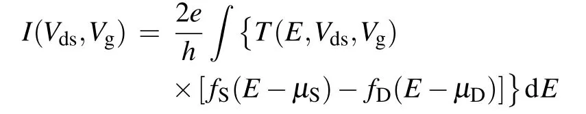
The corresponding transmission spectra of DG SBFETs based on 2D SiC with ML and BL 1T-phase MoS2contacts are shown in Fig.3. The gate and bias voltages are set as zero.The detail geometric structures of AA-stacked, AB-stacked and AC-stacked BL 1T-phase MoS2are shown in Figs.3(b)-3(d).One can find that there is a energy gap of 2.64 eV in every transmission spectrum,which originates from the band gap of 2D SiC(2.64 eV).Moreover,transmission coefficients around the valence band maximum (VBM) of four DG SBFETs are obviously larger than that around the conduction band minimum(CBM).The energy differences between the Fermi level of 1T-phase MoS2and the VBM of the 2D SiC in the transmission spectrum can be considered as the hole SBH of the DG SBFET.[33]In Fig.3(a), the hole SBH of DG 5.1 nm SBFET based on 2D SiC with monolayer 1T-phase MoS2contact is 1.52 eV. In Fig. 3(b), the transmission spectrum shifts to left relative to the Fermi level of the AA-stacked BL 1T-phase MoS2resulting in the increase of hole SBH to 1.64 eV. For the DG 5.1 nm SBFETs based on 2D SiC with AB-stacked and AC-stacked BL 1T-phase MoS2contacts,the transmission spectra move further to the left by the approximate value resulting in the hole SBH increasing to 1.88 eV and 1.87 eV,as shown in Figs.3(c)and 3(d). In addition,the transmission coefficients around the CBM will also show the significant reductions. In other words,bilayer 1T-phase MoS2contacts will greatly affect the SBH and the electronic transport properties of devices compared to ML 1T-phase MoS2contact.The main reason for the changes of the SBH is the different Fermi levels of the bilayer 1T-phase MoS2 contacts under different stacked structures.
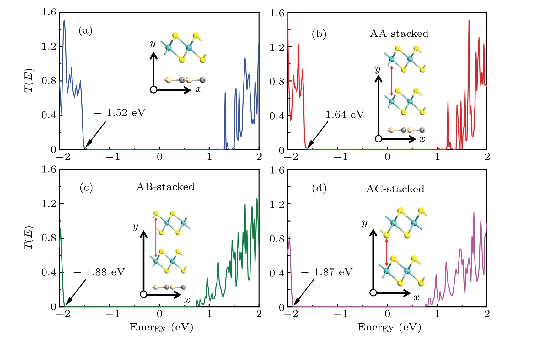
Fig.3. (a)Zero bias transmission spectrum of DG SBFET based on 2D SiC with ML 1T-phase MoS2 contact. Zero bias transmission spectra of DG SBFETs based on 2D SiC with(b)AA-stacked,(c)AB-stacked and(d)AC-stacked BL 1T-phase MoS2 contacts.
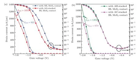
Fig.4. (a)Transfer characteristics of DG SBFETs based on 2D SiC with ML 1T-phase MoS2 contact and AA-stacked BL 1T-phase MoS2. (b)Transfer characteristics of DG 5 nm SBFETs based on 2D SiC with AB-stacked and AC-stacked BL 1T-phase MoS2. ON-state currents are shown in all the figures.
Figure 4 shows the transfer characteristics in linear and logarithmic forms of all DG SBFETs based on 2D SiC with ML or BL 1T-phase MoS2contacts. OFF current (IOFF) is set at 0.1 µA/µm, and ON-state current (ION) must be larger than 900µA/µm following the stander required by ITRS(2013 version). In the transfer characteristics, the ON-state current corresponds to the current at the gate voltage ofVON(VON=VOFF+VDD).VOFFis the gate voltage ofIOFFandVDDis the supply voltage(0.64 V).In Fig.4(a),the drain current of DG SBFETs based on 2D SiC with monolayer MoS2contact is lower than 10−7µA/µm on zero gate voltage. After applying negative gate voltage, the drain currents will increase slowly first and then rise rapidly after−0.3 V gate voltage. The ON-state current is 921 µA/µm, is slightly higher than the standard required by HP application (900 µA/µm).In addition, the drain currents of DG SBFETs based on 2D SiC with AA-stacked BL 1T-phase MoS2contact also increase slowly first and then rise rapidly after−0.5 V gate voltage.In Fig. 4(a), one can find that the threshold swing value (describing the gate-control ability) of DG SBFETs with AAstacked BL 1T-phase MoS2contact is obviously lower than that of DG SBFETs with ML 1T-phase MoS2contact. Thus,the corresponding ON-state current is 1054µA/µm,which is higher than that of DG SBFETs with ML 1T-phase MoS2contact. However,in Fig.4(b),the threshold swing values of DG SBFETs with AB-stacked and AC-stacked BL 1T-phase MoS2contacts are nearly same with each other. The corresponding ON-state currents are slightly different,even though they have the similar hole SBHs. The ON-state current of DG SBFET with AB-stacked BL 1T-phase MoS2contact is 979 µA/µm.The ON-state current of DG SBFET with AC-stacked BL 1Tphase MoS2contact is 1202 µA/µm, which is largest in four DG SBFETs. Although the BL metallic 1T-phase MoS2contacts in three stacked structures have different effects on the transfer characteristics of DG 2D SiC SBFETs, they all can further raise the ON-state currents of DG SiC-SBFETs compared to the device with the ML 1T-phase MoS2contact.

Fig. 5. Spectral currents and LDOS of DG SBFETs based on 2D SiC with(a)monolayer 1T-phase MoS2 contact and(b)AA-stacked BL 1Tphase MoS2 at ON-state gate voltages.
In order to explore the different transfer characteristics of DG SBFETs based on 2D SiC with ML and BL 1T-phase MoS2contacts,we perform analyses on their spectral currents and local density of state (LDOS) at ON-state gate voltages in Figs. 5 and 6. Here, one can see that there is the obvious direct tunneling through the barriers resulting in the drain currents. So, one can find there are three spectral current peaks in the region between theEF(S)andEF(D)leading to the high currents in Fig. 5(a). Although the DG SBFET based on 2D SiC with AA-stacked BL 1T-phase MoS2contact has a larger hole SBH compared to that of the DG SBFET based on 2D SiC with ML1T-phase MoS2contact,the corresponding three spectral current peaks are higher than that of the DG SBFET based on 2D SiC with ML 1T-phase MoS2contact as shown in Fig.5(b). Consequently, the DG SBFET based on 2D SiC with AA-stacked BL 1T-phase MoS2contact has a larger ONstate current (1054 µA/µm) than the ON-state current of the DG SBFET based on 2D SiC with ML 1T-phase MoS2contact (921 µA/µm). The reason for the increase of ON-state current is that the AA-stacked BL 1T-phase MoS2contact has the larger DOS which can provide more incoming wave functions from the source region to the drain region.
For the DG SBFET based on 2D SiC with AB-stacked and AC-stacked BL 1T-phase MoS2contacts, there are two direct tunneling passageways aroundEF(D) to dominate the drain currents at the ON state resulting in two spectral current peaks in the region between theEF(S) andEF(D) as can be seen from Fig. 6. In Fig. 6(a), two spectral current peaks are nearly the same as high values leading to the big ON-state current (1202 µA/µm) for the DG SBFET based on 2D SiC with AB-stacked BL 1T-phase MoS2contact. Although there still two spectral current peaks for the DG SBFET based on 2D SiC with AC-stacked BL 1T-phase MoS2contact in the region between theEF(S) andEF(D), one of them has a similar large value and the other has a small value compared to that of the DG SBFET based on 2D SiC with AB-stacked BL 1T-phase MoS2contact as shown in Fig. 6(b). As a result,the ON-state current(979µA/µm)is lower than the ON-state current of DG SBFET based on 2D SiC with AB-stacked BL 1T-phase MoS2contact. In other words, the AB-stacked BL 1T-phase MoS2contact has the larger DOS than that of ACstacked BL 1T-phase MoS2contact, which can provide more incoming wave functions from the source to the drain resulting in the higher ON-state current. The bilayer metallic 1T-phase MoS2contacts in three stacking structures all can further raise the ON-state currents of DG SiC-SBFETs in varying degrees.

Fig. 6. Spectral currents and LDOS of DG SBFETs based on 2D SiC with(a)AB-stacked and(b)AC-stacked BL 1T-phase MoS2 at ON-state gate voltages.
Benchmarks of performance of DG SBFETs based on 2D SiC with ML and AA-stacked, AB-stacked, AC-stacked BL 1T-phase MoS2contacts are shown in Table 1. ON-state currents (ION/IOFF) of DG SBFETs based on 2D SiC with ML and AA-stacked, AB-stacked, AC-stacked BL 1T-phase MoS2contacts are 921 µA/µm (9.21×10³), 1054 µA/µm(1.054×104), 1202 µA/µm (1.202×10⁴), and 979 µA/µm(9.79×103), which all overstep the stander of HP FET for the production year 2028. The intrinsic gate capacitanceCgis calculated from the equation ofCg=∂Qch/∂VG.[34]Table 1 shows that theCgvalues of four DG SBFETs are 0.181 fF/µm,0.206 fF/µm,0.235 fF/µm,and 0.186 fF/µm. This shows that parametersCgof four FETs are also very satisfactory. In addition, the dynamic power indicator (DPI) and the intrinsic transistor delay timeτare considered as the two other important FET parameters of merit, reflecting the energy and time the FET needs to switch. The DPI per width is calculated by the formula of DPI=(Cg×V2dd)/W, whereWis the channel width.[34]The intrinsic transistor delay timeτcan be calculated by the formulaτ=(Cg×Vdd)/Ids.[34]One can see from Table 1 that the DPIs of four DG SBFETs are 0.074 fJ/µm,0.084 fJ/µm,0.096 fJ/µm,and 0.077 fJ/µm,respectively. Although there are slight differences from each other, the DPIs of four DG SBFETs are far below the standard of the ITRS requirement.The intrinsic transistor delay times of four SBFETs are 0.126 ps, 0.125 ps, 0.125 ps, and 0.122 ps, which are all less than the ITRS (2013 version) requirement of HP FET(0.423 ps). Moreover,one can see that the intrinsic transistor delay times of four SBFETs are nearly same with each other.In other words,the intrinsic transistor delay time is a stable parameter for DG SBFETs based on 2D SiC whatever with ML 1T-phase MoS2contact or with BL 1T-phase MoS2contacts under the different stacked structures.
Table 1. Benchmarks of performance for DG SBFETs based on 2D SiC with ML and AA-stacked, AB-stacked, AC-stacked BL 1T-phase MoS2 contacts relative to the HP devices standers of the next decades.
4. Conclusion
In summary, we have preformed a first-principles study of performances of 5 nm double-gated(DG)Schottky-barrier field effect transistors (SBFETs) based on two-dimensional SiC with monolayer or bilayer metallic 1T-phase MoS2contacts. Because of the wide bandgap of SiC, the corresponding DG SBFETs of 2D SiC with monolayer 1T-phase MoS2contact can weaken the short channel effect. The calculated transfer characteristics also meet the standard of the high performance transistor summarized by ITRS.The corresponding ON-state current is 921µA/µm,which is slightly higher than the standard required by HP application(900µA/µm). Moreover, the bilayer metallic 1T-phase MoS2contacts in three stacking structures all can further raise the ON-state currents of 5 nm DG SiC-SBFETs in varying degrees. The ON-state current of DG SBFET with AC-stacked BL 1T-phase MoS2contact is 1202µA/µm,which is largest in four DG SBFETs.The intrinsic gate capacitance, the dynamic power indicator and the intrinsic transistor delay time of our 2D SiC DG SBFETs are all better than the standard summarized by ITRS.Hence, the above results are very helpful and instructive for the design of short channel transistors in the future.
猜你喜欢
杂志排行

Chinese Physics B的其它文章
- Numerical investigation on threading dislocation bending with InAs/GaAs quantum dots*
- Connes distance of 2D harmonic oscillators in quantum phase space*
- Effect of external electric field on the terahertz transmission characteristics of electrolyte solutions*
- Classical-field description of Bose-Einstein condensation of parallel light in a nonlinear optical cavity*
- Dense coding capacity in correlated noisy channels with weak measurement*
- Probability density and oscillating period of magnetopolaron in parabolic quantum dot in the presence of Rashba effect and temperature*