Numerical investigation on threading dislocation bending with InAs/GaAs quantum dots*
2021-11-23GuoFengWu武国峰JunWang王俊WeiRongChen陈维荣LiNaZhu祝丽娜YuanQingYang杨苑青JiaChenLi李家琛ChunYangXiao肖春阳YongQingHuang黄永清XiaoMinRen任晓敏HaiMingJi季海铭andShuaiLuo罗帅
Guo-Feng Wu(武国峰) Jun Wang(王俊) Wei-Rong Chen(陈维荣) Li-Na Zhu(祝丽娜)Yuan-Qing Yang(杨苑青) Jia-Chen Li(李家琛) Chun-Yang Xiao(肖春阳)Yong-Qing Huang(黄永清) Xiao-Min Ren(任晓敏) Hai-Ming Ji(季海铭) and Shuai Luo(罗帅)
1State Key Laboratory of Information Photonics and Optical Communications,Beijing University of Posts and Telecommunications,Beijing 100876,China
2Center of Materials Science and Optoelectronics Engineering,University of Chinese Academy of Sciences,Beijing 100049,China
Keywords: InAs/GaAs quantum dots,threading dislocation,finite element method,bending area
1. Introduction
With the advent of the era of big data and the rapid growth of internet information,communication networks are required to develop towards the high speed and large capacity.[1,2]Owing to the limitation of transmission bandwidth and power consumption, the traditional electrical interconnection cannot meet the development requirements for high-performance chips, and integrated optical interconnection on Si platform is considered as one of the effective ways to solve these problems.[3,4]As the core device of optoelectronic integration,heteroepitaxial laser on GaAs/Si template can integrate the advantages of the two materials to realize the Si-based monolithic integration of microelectronic devices and the GaAsbased optoelectronic devices,and it is widely used in the high bandwidth optical interconnection field.[5,6]
However, the GaAs/Si heteroepitaxy encounters many difficulties, in which the major bottleneck problem required to be solved is the high-density threading dislocations (TDs)due to the substantial difference in lattice constants between the two materials. If there are a large number of dislocations in the epitaxial layer, the minority carriers will form non-radiation recombination before the population inversion,which will seriously affect the performance of laser.[7]Therefore, it is necessary to take measures to reduce the density of TDs.In the past 40 years,various methods have been proposed for TD bending, such as thermal cyclic annealing, patterning substrates, and using strained-layer superlattices (SLS) and QDs.[8-14]Compared with SLS, QDs have strong stress field as three-dimensional stress structures. A very strong Peach-Koehlor force will bend the dislocation energetically when a TD propagates close to a QD.[15-18]
To reduce the TD density, the design of QD dislocation filters has attracted extensive attention. Experimentally,Wanget al. measured the dislocation density to be about 2×106cm−2by inserting five-layer InAs QDs dislocation filters into GaAs/Si film while the the dislocation density is 5×107cm−2in the sample without QDs.[19]By the theoretical analysis and further optimizing the experimental condition,Huet al. reduced dislocation density from 3×106cm−2to 9×105cm−2by combining the insertion of three-layer InAs QDs dislocation filters with the three-step growth method.[20]Theoretically,Yeet al.analyzed the TD bending in GaN/AlN QDs by using the finite element method(FEM),in which the misfit strain introduced by the edge dislocation is modeled by feeding Eshelby strain into this system.[21]Yanget al. used the position independent model (PIM) to calculate the bending area ratio of single InxGa1−xAs/GaAs QD.[18]Zhouet al.investigated the effect of InxGa1−xAs/GaAs QDs component on the obstruction of TDs by adopting FEM model.[22]
In short, the dislocation density is reduced with using the embedded QDs dislocation filter, and the TD bending is observed by transmission electron microscopy (TEM). However,the effect of dislocation filters cannot be anticipated before the crystal growth. Evaluating the bending capability can not only help us to improve the performance of QD dislocation filters thereby avoiding the poor effect in experiment,but also shorten the experiment time and reduce cost. Whereas according to the reports,the theoretical study about edge dislocation is unsuitable for the analysis of TD bending in a GaAs/Si epitaxial system. The position of TD is ignored by the PIM method,but its position plays an important role in determining the elastic strain energy.[23]More importantly,these researches are limited to single QD, which cannot provide enough help for the design of dislocation filters in experiment.
From what has been discussed above, in this study, the full consideration is devoted to the influence of dislocation position, and the finite element method (FEM) is used to establish the three-dimensional (3D) model of 60°TD, and the critical condition for TD inclination is studied. What is more,the method to evaluate the bending capability of single-layer QDs and multi-layer QDs is proposed.
In the first part of this paper, the critical position for TD bending is determined by the FEM calculation.Next,the influence of cap layer thickness and QD base width are discussed,and the results indicate that the increase of them makes positive contribution to TD bending. Finally, the bending area ratio of single-layer QDs and the dislocation blocking ratio of multi-layer QDs (TDs impeded by QDs dislocation filter divide by the initial TDs)are predicted.
2. Model and methods
The previous researches show that the boundary effect can be effectively avoided if the volume of the substrate is much larger than QD,and the initial stress in the substrate can also be considered to be zero.[24-26]Therefore,we establish a cubic GaAs substrate with a size of 100 nm×100 nm×100 nm including 0.3-nm wetting layer(usually 1~2 monolayers[24]).A 4-nm-high tapered InAs QD is located in the center above the substrate. The width of the QD ranges from 8 nm-24 nm,and the thickness of cap layer is 5 nm. Note that the effect of cap layer thickness will be studied in the later section,in which the different thickness is also analyzed. In our work,Cartesian coordinates are adopted and the origin is seated the center of the substrate bottom. TheXaxis,Yaxis, andZaxis represent[110],[-110],and[001]directions,respectively,whereZdirection is the growth direction of QD as shown in Fig.1.
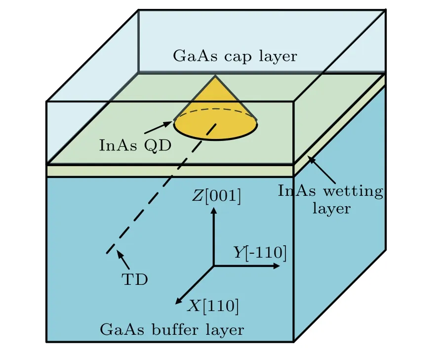
Fig.1. Geometrical model of InAs/GaAs QD.
Assume that there are two cases (1: TD enters into QD,2: TD inclination occurs), as shown in Fig. 2. The elastic strain energy of the whole structure is calculated by varying the arrival position of TD in QD base width. Then the critical position and the bending area ratio of single QD can be obtained when the energy of the two systems is equal.

Fig.2. Two cases when TD arrives at base of QD.
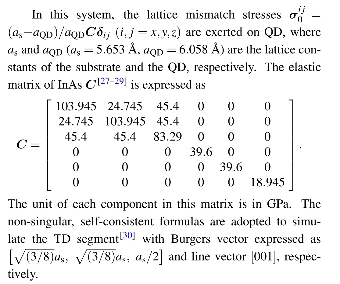
There is the stress caused by lattice mismatch and the stress induced by TD when TD enters into QD. The wellknown equation is adopted to calculate the elastic strain energy of the system.[22,27,31]In addition to the above two kinds of stress sources, the stress induced by MD should be taken into consideration,and thus the equation needs adjusting appropriately[22,31]and the corresponding elastic strain energy in this system can be computed. To make the solution convergent,the appropriate boundary conditions are imposed,and a reasonable numerical value is obtained.
Through the calculation of the critical condition, we can obtain the bending area ratioAof single QD and the bending area ratio of single-layer QDM1is inferred to be

whereSis the base area of single QD, andρis the density of QDs. Assuming that the TDs are uniformly distributed in the GaAs substrate and TD inclination occurs only when it reaches close to QD (neglecting the stress released by QDs formation[24]and the interaction between TDs), the dislocation blocking ratio ofn-layer QDs dislocation filterMncan be calculated from the following equations:
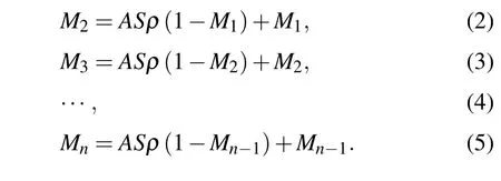
Based on the above equations, the relationship between the number of the QDs layer and the blocking dislocation ratio can be speculated.
3. Results and discussion
In this section, the relationship between dislocation position and the elastic strain energy of InAs/GaAs QDs in the two isolated systems is explored. Then the effects of the cap layer thickness and the base width are investigated. Finally,the bending capability of the single-layer QDs and the multilayer QDs are discussed.
As shown in Fig. 3, the corresponding elastic strain energyEthr(the elastic strained energy of the system when TD enters into QD)andEmis(the elastic strained energy of the system when TD inclination occurs) for a QD with 20-nm base width are calculated by changing the arrival position of TD from center to the boundary of the QD along theX-axis direction. When the TD enters into the QD without MD formation(the black curve as shown in Fig.3),it can be seen that the energy is significantly affected by the position TD reaching and it decreases as TD approaches to the edge of the QD. While the energy tends to fluctuate up and down slightly when TD inclination occurs (the red curve as shown in Fig. 3). Two curves intersect at 9 nm,which is considered to be the critical position. The left side of the intersection represents QD bending TD into interfacial MD, and then the bending area ratio(about 81%) can be further obtained. It is found that the TD bending occurs more easily when it reaches the center region of the QD.We speculate that this is due to the force QD loading on TD in the central region is stronger than that in the edge region,and MD is energetically favorable in this region.
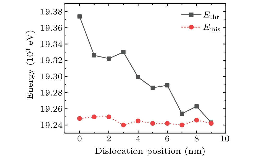
Fig.3. The relationship of the stain energies Ethr and Emis with the dislocation position.
In order to explore the influence of cap layer thickness for TD bending,we fix the critical position in a range from 9 nm to 9.8 nm,then the cap layer thickness is adjusted to makeEthrandEmisequal.It is indicated in Fig.4 that the thickness of cap layer needs increasing with the critical position moving rightward. With the bending area ratio of single QD raised from 81%to 96%,the required thickness must increase from an initial value of 5 nm to 9.2 nm. And the computations show thatEthris much larger thanEmisin the whole range of QD base when the thickness of cap layer exceeds 10 nm. The result shows that heightening the thickness of cap layer can benefit the inclination of TD energetically,and this thickness selected in experiment to be almost more than 20 nm[18-20]is perfect enough.
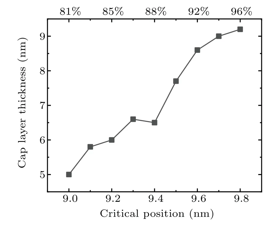
Fig.4. Relationship between cap layer thickness and critical position.
Varying the base width from 8 nm to 24 nm and considering the 5-nm cap layer thickness, theEthrandEmisare calculated,and the results show that the relationship between the base width of QD and the bending area ratio of single QD is obtained. It can be seen from Fig.5 that the bending area ratio shows an overall upward trend in this interval,but a slight decrease at 14 nm. This ratio increases rapidly from 8 nm to 12 nm, and it goes up steadily from 14 nm to 20 nm. Within the range of the base width, the maximum bending area ratio reaches 85.56%. The changing pattern is well consistent with the analytical results[20](red points in the figure). However,there are some differences in quantitative value since we take TD position and cap layer into consideration.
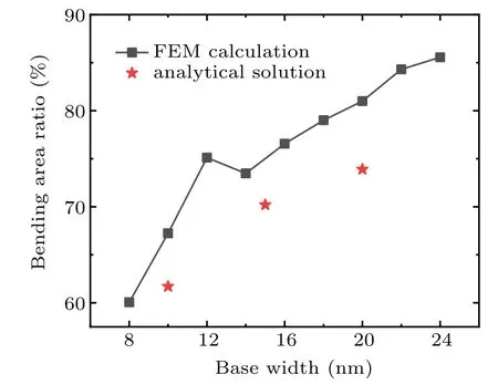
Fig. 5. The relationship between bending area ratio and base width of the single QD.
By using Eq.(1)and taking the density of 1011cm−2into account, the bending area ratioversusbase width of singlelayer QDs is calculated and shown in Fig.6. The result shows that the bending area ratio keeps an upward tendency when the base width increases from 8 nm to 24 nm, and it rises up first slowly then rapidly in this range. The bending area ratio reaches its maximum value at 24 nm,i.e., roughly 38.71%.This is similar to the calculation result reported previously[20](red points in the figure).
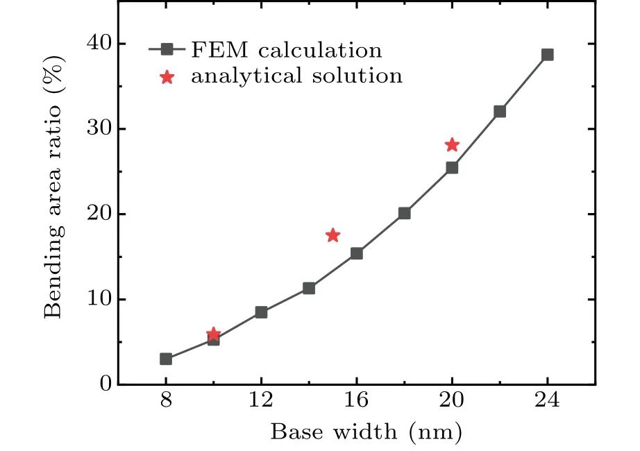
Fig. 6. Relationship between bending area ratio and base width of QD of single-layer QD.
Also following Eqs.(2)-(5), the dislocation blocking ratio is predicted with taking a base width of 24 nm. The results are shown in Fig. 7, indicating that the dislocation blocking ratio increases with the layer number of QDs rising from one to five.But unlike the bending area ratio of single layer,the increase is gradually slow down and tends to be saturated.When the number of the layers is five, the blocking dislocation ratio rises up to 91.35%. This regular pattern demonstrates that about 3-5 embedded QD layers can reduce the QDs density sufficiently, which can be proven by the previous experimental results.[19,20]

Fig.7. The relationship between blocking dislocation ratio and layer number of QD.
4. Conclusions
In this work, the TD bending with InAs/GaAs QDs is studied.The results show that TD bending is more likely to occur in the central area of QDs,and its critical position is about 9 nm,corresponding to the height and width of the QD of 4 nm and 20 nm, respectively. The TD bending can be strengthened by increasing the cap layer thickness and the base width.In addition, the method to calculate the bending area ratio of single-layer QDs and the blocking dislocation ratio of multilayers QDs are proposed.For QDs with a density of 1011cm−2and a base width of 24 nm, the bending area ratio of singlelayer QDs reaches 38.71%,and the blocking dislocation ratio rises up to 91.35%when using the five-layer embedded QDs.This research can accurately evaluate the bending effect at the beginning of the experiment, and thus providing reasonable guidance for designing the QD dislocation filter.Although this study is about 60°TD with InAs/GaAs QD,its method is also applicable to other systems with reasonable modification.
猜你喜欢
杂志排行

Chinese Physics B的其它文章
- Connes distance of 2D harmonic oscillators in quantum phase space*
- Effect of external electric field on the terahertz transmission characteristics of electrolyte solutions*
- Classical-field description of Bose-Einstein condensation of parallel light in a nonlinear optical cavity*
- Dense coding capacity in correlated noisy channels with weak measurement*
- Probability density and oscillating period of magnetopolaron in parabolic quantum dot in the presence of Rashba effect and temperature*
- Hardware for multi-superconducting qubit control and readout*