Vertical GaN Shottky barrier diode with thermally stable TiN anode∗
2021-03-19DaPingLiu刘大平XiaoBoLi李小波TaoFeiPu蒲涛飞LiuAnLi李柳暗ShaoHengCheng成绍恒andQiLiangWang王启亮
Da-Ping Liu(刘大平), Xiao-Bo Li(李小波), Tao-Fei Pu(蒲涛飞),Liu-An Li(李柳暗), Shao-Heng Cheng(成绍恒), and Qi-Liang Wang(王启亮),§
1Department of Physics,Xinxiang University,Xinxiang 453003,China
2Institute of Technology and Science,Tokushima University,Tokushima 770-8506,Japan
3School of Electronics and Information Technology,Sun Yat-Sen University,Guangzhou 510275,China
4State Key Laboratory of Superhard Material,Jilin University,Changchun 130012,China
Keywords: GaN,Vertical Schottky barrier diode,TiN,interface quality
1. Introduction
Gallium nitride(GaN)is suitable for high power applications because of its high critical electric field and mobility.[1,2]Compared with the lateral AlGaN/GaN structure, the vertical geometry devices are more promising due to high current levels and better thermal management.[3,4]Especially, freestanding GaN substrates with significantly low threading dislocation density(104-105cm−2)have been achieved over the past decade. GaN-on-GaN based power rectifiers, such as Schottky barrier diodes (SBDs) and PN diodes (PNDs), have achieved remarkable progress as compared to those fabricated on heteroepitaxial GaN materials. Therefore,the vertical GaN devices have been considered as a good candidate for nextgeneration power modules.[5]
Commonly,metal electrodes(Ni,Pt,Cu,etc.) with relatively high work function are adopted as the Schottky contact on GaN to decrease the reverse leakage current.[6-8]However,the interface reaction occurs between the metal and GaN and causes the degradation of the rectification characteristics.[9]In our previous work,[10]the Ni/GaN SBD shows a relatively large Schottky barrier height(SBH,Φb)of 0.87 eV along with a relatively large ideality factor(n)of 1.23. In addition,the reverse current leakage is much higher than the theoretical value calculated from the thermionic emission(TE)model. The increase of leakage current is attributed to the defect-assisted tunneling caused by the interaction at Ni/GaN interface.[9]By introducing nitrogen during the reactive sputtering of Ni, we confirmed that the formation of NiN is effective to suppress the interface reaction and to enhance the thermal stability.[11]On the other hand,the reactively-sputtered TiN anode SBD shows smaller Φband n of 0.59 eV and 1.07,respectively. However,the reverse leakage is comparable with Ni,implying the good interface status.
Furthermore, the thermal stability of Ni and TiN anode SBDs were evaluated by temperature-dependent currentvoltage (I-V) characteristics.[12]The temperature was adjusted to 25◦C, 75◦C, 25◦C, 125◦C, 25◦C, 175◦C, and 25◦C, consecutively. The turn-on voltage and on-resistance(Ron) deduced from the linear plot remain virtually constant for all the data at 25◦C. However, obvious current fluctuation is observed from the logarithm plot for the Ni anode diode in the threshold voltage region. In the reverse biased region, the leakage current of Ni diode presents weak temperature-dependence and increases after the temperature returned to 25◦C. On the other hand, the leakage current of TiN SBD shows a better thermal stability and is dominated by thermionic emission. Finally, the TiN also serves as the gate material of AlGaN/GaN HFETs, maintaining good Schottky properties even after the ohmic annealing at 800◦C.[13]Those results demonstrated that the TiN is a promising anode material for GaN SBD compared with Ni.
Recently,the TiN anode is used to fabricate vertical SBD for power rectifier and temperature sensor applications. However, the electrical performance and interface quality of the TiN/GaN diode are not investigated extensively. In this work,a vertical GaN SBD with TiN anode was fabricated and the interface quality was also evaluated. The temperature dependent I-V characteristics confirm the good thermal stability of TiN/GaN contact under temperatures from 25◦C to 200◦C.In addition, the rectifying characteristics are interpreted by the TE theory, presenting a barrier height inhomogeneous behavior. Finally, by combining the low-frequency noise and frequency-dependent capacitance-voltage(C-V)measurements,good interface status of TiN/GaN is demonstrated.
2. Device fabrication and process
The 14-µm n−-GaN drift layer was grown on a commercial GaN substrate by metal-organic chemical vapor deposition. The 2-inch free-standing substrate presents a thickness of 350-µm and a resistivity of 0.05 Ω·cm. The fabrication of the vertical SBD (Fig.1) adopted a standard lift-off process. After cleaning, an optimized structure of Ti/Al/Ti/Au(50/200/40/40 nm) was sputtered and annealed in N2ambient at 800◦C for 1 min to form the ohmic contact. Then,a 1 µm-thick Au layer by gold electroplating was adopted to improve the contact between probe and electrode.After cleaning in a BHF and a diluted HCl solution, circular TiN/Ni/Au(100/30/30 nm) Schottky anode with a diameter of approximately 140 µm was formed by reactive sputtering. The TiN film was sputtered in Ar:N2(15:3 sccm)mixed gas atmosphere under 0.14 Pa, using a Ti target.[10,12]To improve the contact homogeneity between the sputtered metal layers and GaN,post deposition annealing was conducted at 300◦C for 10 min.
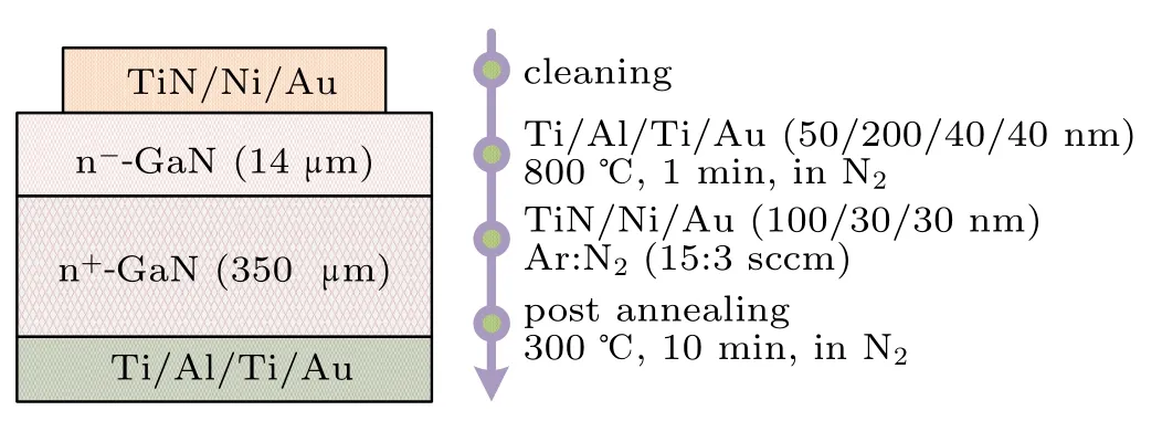
Fig.1. Schematic view of the fabricated vertical GaN Schottky barrier diode and the corresponding main device process.
3. Results and discussion
The room-temperature I-V and C-V characteristics of the SBD were measured as shown in Fig.2. Based on the linear extrapolation method, a turn-on voltage (Von) of approximately 0.41 V was obtained with a differential specific Ronof approximately 0.98 mΩ·cm2(Fig.2(a)).The maximum capacitance at zero bias is approximately 14 pF in theC-V curve(inset of Fig.2(b))and decreases with the increasing reverse bias.In addition,the Φband donor concentration are approximately 0.68 eV and 2.08×1016cm−3,calculating from the slope and intercept of 1/C2versus V plot (not shown). The relatively smaller SBH compared with the conventional electrodes (Ni or Pt)is helpful to realize a smaller Von,which is beneficial for reducing the power loss in on-state. The depth profile of carrier density along the vertical direction is extracted from the C-V curve as shown in Fig.2(b). The net doping concentration of the drift layer is close to 2.08×1016cm−3, which is consistent with the 1/C2-V results.
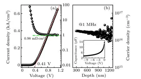
Fig.2. The forward I-V characteristics(a)and the corresponding carrier concentration depth profile(b)of the SBD.Inset of(b)is the C-V characteristic.
To evaluate the thermal stability of the TiN/GaN contact,we measured the I-V characteristics at different prober stage temperatures from 25◦C to 200◦C with steps of 25◦C.After high temperature measurement,the sample was cool down to 25◦C and the I-V characteristic was recorded again to confirm that there is no obvious degradation. This result implies the good TiN/GaN interface status and good thermal stability.Observed from the semi-logarithm I-V plots(Fig.3(a)),the SBD presents a temperature-dependent rectification characteristic.In the reverse biased region, the leakage current increases about 3 orders of magnitude from 10−7A to 10−4A when the temperature increases to 200◦C.However,for the forward biased region (Fig.3(b)), the voltage decreases linearly with the increasing temperature at a specific current level. Furthermore, the temperature-dependent variation of Φbwith n are fitted using the TE model. When VF>3 kT/q, the forward current(ID)can be expressed as[14,15]
where Ae, T, q, n, k, A∗and Rsare the Schottky anode area,Kelvin temperature, electronic charge, ideality factor, Boltzmann constant, Richardson constant (26.9 A·cm−2·K−2) and series resistance, respectively. The obtained Φb(n) increases(decreases)with increasing temperature,respectively. The linear relationship between n and Φbis attributed to the effect of barrier height inhomogeneous as discussed in our previous work[12,16](inset of Fig.3(b)).
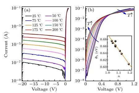
Fig.3. The semi-logarithm plots of the temperature-dependent rectification characteristic (a) and the forward region (b). Inset of (b) gives the relationship between SBH and n.
The breakdown voltage of the vertical diode was approximately 100 V as shown in Fig.4(a). The relatively lower breakdown voltage is ascribed to the relatively smaller work function of TiN, which results in a relatively smaller Schottky barrier height. Although it can help to decrease the Von,the relatively higher reverse leakage current of TiN-anode SBD(compared with the conventional Ni/Au or Pt anode)decreases the breakdown voltage.Effective termination structure is needed to suppress the leakage current in future design. A double-pulse test circuit with an inductive load (shown in inset of Fig.4(b))was adopted to measure the reverse recovery characteristics of vertical diodes(without package). When the first pulse turned on the metal-oxide-semiconductor field effect transistor (MOSFET), the inductor was charged by the power supplier whereas the device under test (DUT) was reversely biased. Then, the DUT worked in the forward region during the MOSFET was turned off. Finally,the second pulse signal turned on the MOSFET again and the reverse characteristics of the DUT were recorded. The SBD was switched from on-state(about 300 mA)to off-state at a bias of −30 V.From Fig.4, the reverse recovery time (defined as the time when the reverse current decreased to 10% of the maximum current)is approximately 25 ns. By integrating the area under the reverse current over the period of reverse recovery time,the corresponding reverse recovery charge was calculated to be approximately 0.56 nC.
Low-frequency noise measurement is a powerful method to understand the interface characteristics of TiN/GaN Schottky contact. By applying different forward currents across the diode, the spectral power density of current fluctuations(SI) are calculated from the voltage fluctuations (SV). It is found that the SIof the SBD follows a 1/f behavior and increases with the increasing current level (as shown in Fig.5(a)). Generally,if the transport is dominated by a single trap level, the noise should be Lorentzian type based on the‘mobility fluctuations’or‘number fluctuations’model.Therefore, the 1/f behavior is ascribed to the multiple traps as well as the existence of barrier inhomogeneous at TiN/GaN interface.[17]The interface status can be further investigated by the frequency-dependent C-V measurements.The C-V curves were recorded in the frequency range from 1 kHz to 1 MHz to confirm the trapping effects (Fig.5(b)). When the negative bias on the diode is relatively smaller,there is no obvious capacitance dispersion even at a high frequency of 1 MHz. On the other hand,the capacitance dispersion is enhanced slightly with the increasing reverse voltage.[18]
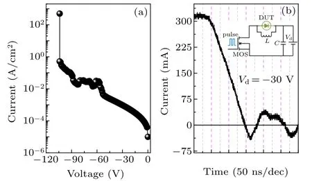
Fig.4. The reverse breakdown (a) and recovery (b) characteristics of diode measured with a double-pulse test circuit(as shown in inset).
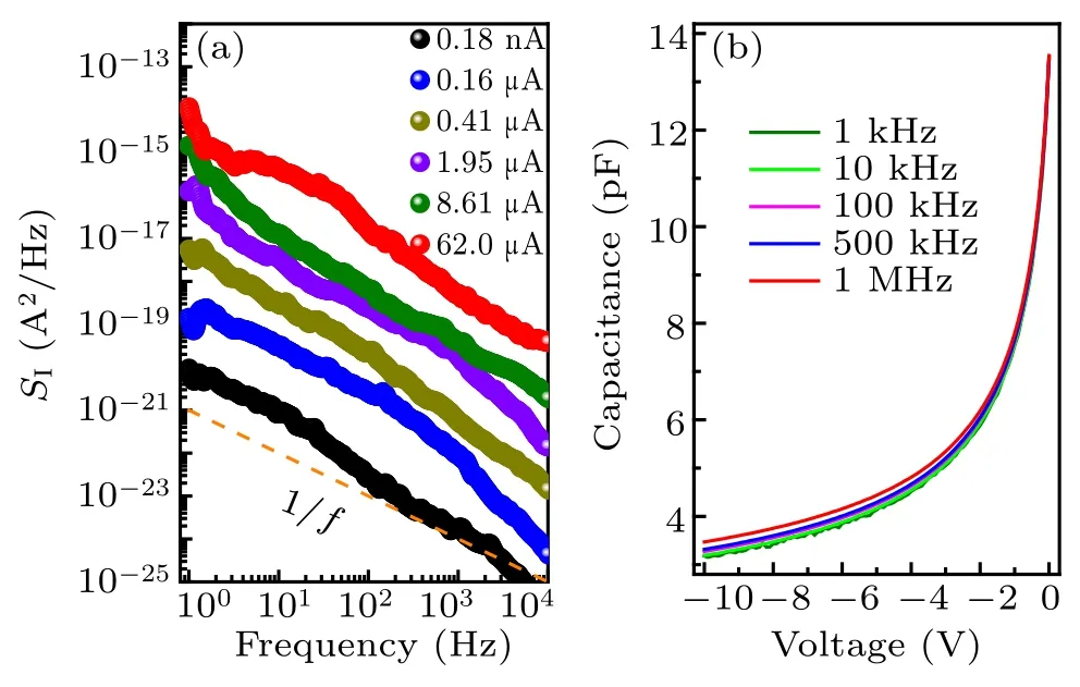
Fig.5.The low-frequency noise forward currents(a)and the frequencydependent C-V measurements(b)of SBD.
The possible mechanism of the frequency dispersion can be explained from the band diagram as shown in Fig.6. When the Schottky contact under zero bias or relatively small reverse bias (Fig.6(a)), most of the interface states are below the Fermi level and only the shallower interface traps close to the Fermi level respond to the signal.The relatively small time constant of the shallower interface traps can follow up the variation of frequency,resulting in a very weak frequency dispersion phenomenon.When the reverse bias increased(Fig.6(b)),the Fermi level downshifted in the GaN side and the electrons on shallow traps would de-trap. Then, the deeper interface traps can not follow up the variation of frequency,resulting in a slight frequency dispersion effect. Therefore,the dispersion effect of vertical GaN SBD is weak even at the frequency of 1 MHz because of the good interface quality between TiN and GaN.[19]
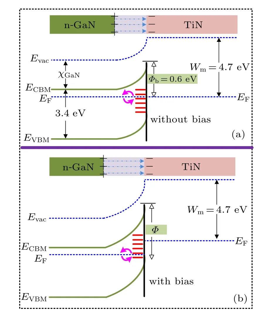
Fig.6. The energy band diagram for TiN/GaN SBD without (a) and with(b)reverse bias. The trapping and de-trapping between traps and Fermi level are marked with purple arrows.
4. Conclusions
In summary, the electrical performance and interface quality of the vertical GaN SBD with TiN anode have been evaluated extensively. The Vonand specific Ronare deduced to be approximately 0.41 V and 0.98 mΩ·cm2,respectively. The relatively smaller Vonis beneficial for reducing the power loss in on-state. Based on the temperature-dependent I-V curves from 25◦C to 200◦C,good rectifying characteristic and good thermal stability are confirmed. Moreover,the rectifying characteristics are interpreted by the TE theory,presenting a barrier height inhomogeneous behavior. The 1/f behavior of lowfrequency noise also indicates the multiple traps and/or barrier inhomogeneous at TiN/GaN interface. The capacitance dispersion under reverse voltage is ascribed to the trapping and de-trapping between traps and Fermi level.Thanks to the good interface quality between TiN and GaN, the dispersion effect of vertical GaN SBD is weak even at the frequency of 1 MHz.
杂志排行

Chinese Physics B的其它文章
- Transport property of inhomogeneous strained graphene∗
- Beam steering characteristics in high-power quantum-cascade lasers emitting at ~4.6µm∗
- Multi-scale molecular dynamics simulations and applications on mechanosensitive proteins of integrins∗
- Enhanced spin-orbit torque efficiency in Pt100−xNix alloy based magnetic bilayer∗
- Soliton interactions and asymptotic state analysis in a discrete nonlocal nonlinear self-dual network equation of reverse-space type∗
- Discontinuous event-trigger scheme for global stabilization of state-dependent switching neural networks with communication delay∗