Two-step growth of β-Ga2O3on c-plane sapphire using MOCVD forsolar-blind photodetector
2024-03-02PeipeiMaJunZhengXiangquanLiuZhiLiuYuhuaZuoandBuwenCheng
Peipei Ma ,Jun Zheng,† ,Xiangquan Liu,Zhi Liu,Yuhua Zuo,and Buwen Cheng
1State Key Laboratory on Integrated Optoelectronics,Institute of Semiconductors,Chinese Academy of Sciences,Beijing 100083,China
2Center of Materials Science and Optoelectronics Engineering,University of Chinese Academy of Sciences,Beijing 100049,China
Abstract: In this work,a two-step metal organic chemical vapor deposition (MOCVD) method was applied for growing β-Ga2O3 film on c-plane sapphire.Optimized buffer layer growth temperature (TB) was found at 700 °C and the β-Ga2O3 film with full width at half maximum (FWHM) of 0.66° was achieved.A metal-semiconductor-metal (MSM) solar-blind photodetector (PD)was fabricated based on the β-Ga2O3 film.Ultrahigh responsivity of 1422 A/W @ 254 nm and photo-to-dark current ratio(PDCR) of 106 at 10 V bias were obtained.The detectivity of 2.5 × 10¹⁵ Jones proved that the photodetector has outstanding performance in detecting weak signals.Moreover,the photodetector exhibited superior wavelength selectivity with rejection ratio(R250nm/R400nm) of 105.These results indicate that the two-step method is a promising approach for preparation of high-quality β-Ga2O3 films for high-performance solar-blind photodetectors.
Key words: MOCVD;two-step growth;β-Ga2O3;solar-blind photodetector;responsivity
1.Introductions
As an emerging wide band gap semiconductor material,β-Ga2O3is considered as one of the most promising materials for power-electronic devices and solar-blind detectors.It is benefit from the excellent material properties ofβ-Ga2O3including ultrawide bandgap (4.6-5.2 eV),high critical field(8 MV/cm),high Baliga’s figure-of merit (3214) and good chemical stability[1-3].β-Ga2O3solar-blind ultraviolet (200-280 nm)photodetectors have wide application owing to their superiorities,such as low background noise,high response value and radioresistance[4,5].In order to improve the photodetector performance,a series of methods are conducted to growβ-Ga2O3films,including molecular beam epitaxy (MBE)[6],halide vapor phase epitaxy (HVPE)[7],low pressure chemical vapor deposition (LPCVD)[8,9],mist chemical vapor deposition (mist CVD)[10]and MOCVD[11].Metal-semiconductormetal (MSM) structure has the advantages of simple fabrication process,convenient integration with readout circuits and high responsivity because of internal gain.Pratiyushet al.[12]demonstrated MSM detector using heteroepitaxialβ-Ga2O3films with a high responsivity of 1.5 A/W.Qianet al.[13]reported MSM detector based on amorphous Ga2O3films with an ultrahigh response of 70.26 A/W and specific detection rate of 1.26 × 10¹⁴Jones.By growing polycrystallineβ-Ga2O3film,Aroraet al.[14]had prepared the high-performance MSM detector with a response of 96.13 A/W.
Althoughβ-Ga2O3film grown by various technologies have been reported,there are still some difficulties in getting ideal qualityβ-Ga2O3films.For example,the expensive substrate for homoepitaxial and the large lattice mismatch for heteroepitaxial.As low-cost substrates,sapphires are widely used in heteroepitaxialβ-Ga2O3films.However,the lattice mismatch betweenc-sapphire andβ-Ga2O3is 3.5%.The stress caused by lattice mismatch will lead to a high dislocation density,which is not conducive to the epitaxial growth of material.In order to alleviate lattice mismatch and improve crystalline quality of epitaxial films,a buffer layer between substrate and epitaxial layer can be applied.However,there are few reports about the effect of buffer layer on the quality ofβ-Ga2O3film onc-sapphire[15,16].
In this work,high-qualityβ-Ga2O3films were grown by two-step MOCVD method onc-sapphire.By varying buffer layer growth temperature,β-Ga2O3film with fullwidth at half maximum (FWHM) of 0.66° was obtained.The MSM solarblind photodetector was fabricated to further verify the excellent performance ofβ-Ga2O3film quality.The solar-blind photodetector exhibits high responsivity of 1422 A/W @ 254 nm.In addition,ultrahigh PDCR (106),detectivity (2.5 × 10¹⁵Jones) and respond speed (36 ms) were also achieved from the fabricated photodetector.This work provides an approach for the preparation of high-qualityβ-Ga2O3films and the application ofβ-Ga2O3solar-blind photodetectors.
2.Experimental details
Fourβ-Ga2O3samples were prepared by depositing oncplane (0001) sapphire in a MOCVD system by the two-step method.First,the thin buffer layer of Ga2O3was deposited at low temperature (TB),and thenβ-Ga2O3film was grown on the buffer layer at 960 °C.Trimethylgallium (TMG) and O2were used as gallium and oxygen precursors,respectively.High-purity argon was used as carrier gas for TMG source.Fourβ-Ga2O3films samples were grown at the same condition,except thatTBwere at 650,700,750 and 800 °C.The crystalline quality ofβ-Ga2O3films were characterized by high-resolution X-ray diffraction (HRXRD,X’Pert3 MRD).The surface morphologies of films were investigated by atomic force microscopy (AFM,SII Nanonavi) and scanning electron microscope (SEM,NanoSEM650).The photodetector with MSM structure was fabricated on theβ-Ga2O3film withTB=700 °C.Si ion implantation process[17,18]was performed and followed by deposition of Ti/Au electrode.After lift-off process,the interdigital electrodes were formed and the rapid thermal annealing at 475 °C for 1 min was conducted.The room-temperature optical responsivities ofβ-Ga2O3PD were measured by an Agilent B1500A semiconductor parameter analyzer and ultraviolet light emitting diodes (UV LEDs) emitting 254 and 356 nm light.Spectral-response measurements at -1 V bias were performed by spectrometer equipped with Xe light source.An Si detector was tested for calibrating the spectrum response.
3.Results and discussion
The crystal property ofβ-Ga2O3films was measured by XRD withω-2θscan mode.Fig.1(a) shows the XRD spectra of Ga2O3films with varyingTBfrom 650 to 800 °C.Three diffraction peaks at 18.9°,38.3°,and 58.9° exhibit well-defined(-201),(-402),and (-603) planes ofβ-Ga2O3,respectively,indicating the (-201) oriented single crystal growth.This is owing to the similar oxygen atomic arrangement of (-201) planeβ-Ga2O3andc-sapphire.The diffraction peak intensity ofβ-Ga2O3film withTB=650 °C is weak,which is likely due to the low migration rate of adsorbed atoms on substrate surface at low growth temperature.When increasingTB,the crystalline quality of epitaxial layer is improved and the intensity of diffraction peak increases.Figs.1(b) gives theωscanning diffraction pattern of (-402)β-Ga2O3planes and the FWHM values at differentTB.The FWHM values of films prepared at differentTBof 650,700,750,and 800 °C are 3.3°,0.66°,0.67°,and 0.93°,respectively.Theβ-Ga2O3films in this work grown by two-step method have much lower FWHM values,compared with previously reportedβ-Ga2O3films on sapphire[19-21].The sample grown atTB=700 °C shows the lowest FWHM value,indicating the optimized buffer layer growth condition is found.
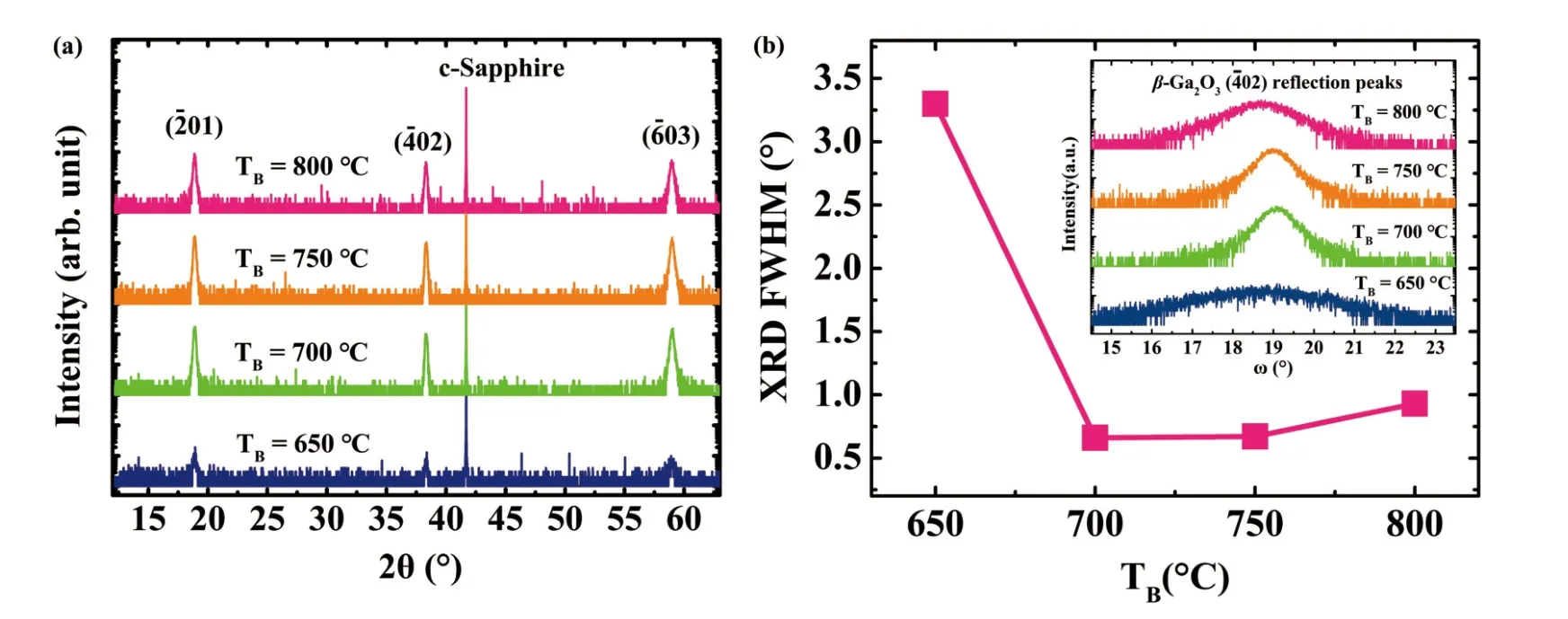
Fig.1.(Color online) (a) XRD ω-2θ scan and (b) FWHM of rocking curve for β-Ga2O3 films grown at different TB.Inset shows the XRD ω scan for films.
AFM was performed to further investigate the surface morphology of films deposited onc-sapphire with differentTB.In Fig.2(a),four samples were examined by AFM scan on a 5 ×5μm scan area.The surfaces of four samples all show regular pseudo-hexagon structures,which are generated by the inplane rotational domains and attributed to the symmetries ofc-sapphire andβ-Ga2O3[22,23].The film withTB=650 °C presents the sparsest texture,which is owing to the low mobility of crystal nuclei during the initial growth and lead to sparse grains difficult to merge.The sample withTB=700 °C exhibits the densest texture,which is likely attributed to the moderate crystal nuclei mobility at this temperature.As the temperature rises (withTB=750 or 800 °C),the atom mobility increases,leading to the deposition of large crystal nuclei on substrates and resulting in rough surfaces.Fig.2(b) shows the surface roughness of four samples,which are 19,6.8,7.5,and 12 nm,respectively.Fig.2(c) gives the variation in film thickness with differentTBand inset shows the cross-sectional SEM image of sample grown withTB=700 °C.The thickestβ-Ga2O3film of 1μm is obtained whenTB=700 °C.These results indicate that the buffer layer temperature at 700 °C is favorable forβ-Ga2O3film two-step growth.
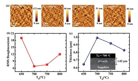
Fig.2.(Color online) (a) AFM images and (b) RMS roughness of β-Ga2O3 films,(c) film thicknesses obtained from the cross-sectional SEM.Inset shows the cross-sectional image of film grown at TB=700 °C.
The MSM solar-blind photodetector was fabricated onβ-Ga2O3film withTB=700 °C.Fig.3(a) shows the optical microscope diagram of device.Fig.3(b) reveals the three-dimensional structure diagram of the device.Fig.3(c) shows theI-Vcharacteristic curve of MSM photodetector.As revealed in figure,the dark current is 400 pA at 10 V bias.Moreover,theI-Vcurve increases only a little under 365 nm light (light intensity of 15 mW/cm2),indicating thatβ-Ga2O3film is not sensitive to 365 nm light.However,theI-Vcurve increases steeply under 254 nm light (light intensity of 1.9 mW/cm2),suggesting strong light response characteristics and excellent solarblind photoelectric characteristics.

Fig.3.(Color online) (a) The optical microscope diagram and (b) structural diagram of MSM photodetector.(c) The I-V characteristics of the MSM photodetector in the dark and illuminated by 254 and 365 nm.(d) The energy band diagram and photogenerated carriers of MSM β-Ga2O3 detector with external bias under 254 nm illumination.
The light/dark current rejection ratio (PDCR)[24],which is defined as (Iphoto-Idark)/Idark,achieves an extremely large value of more than 106,indicating that the device has extremely high sensitivity.The responsivity of MSM detector with effective illumination area about 4.55 × 104μm2reaches 1422 A/W under 10 V bias.Detectivity (D*) can be used to evaluate the ability to perceive the lowest detectable signal,which is related to background noise.Assuming that dark current is the main source of device noise,D* can be expressed as:RS1/2/(2qIdark)1/2[24].The photodetection based on high-qualityβ-Ga2O3film has aD* of 2.5 × 10¹⁵Jones under 254 nm light,indicating the ultra-high signal-to-noise ratio.The excellent wavelength selectivity and ultrahighD* indicate that high sensitivity solar-blind detector is achieved.
Fig.3(d) is energy band diagram and photogenerated carriers of the fabricated MSM photodetector under 254 nm light with external bias.It is determined from carrier transport mechanism that the optical response of photodetector is a complex process.Photogenerated carriers will be captured by deep-level defects so the lifetime is longer than transmission time.Moreover,electrons are quickly swept-out and reinjected to remain electric neutrality,generating multiple electrons and huge photoconductive gain.
The transient response of MSM photodetector under 254 nm wavelength illumination was tested by controlling the turning on and off for the light source,as shown in Fig.4(a).When the light source is turned off,the current of the device decays quickly,showing a fast decay speed.In order to quantitatively analyze the response process of current rise and fall,the time responding characteristics are amplified as shown in Fig.4(b).Then the double exponential relaxation equation is used to fit theI-Tcurve,and the equation is as follows[25]:I=I0+Aexp(-t/τ1)+Bexp(-t/τ2),whereI0is the photocurrent in the stable state,tis the time,AandBare constants,τ1andτ2denote two relaxation time constants.τ1reflects the rapid change of carrier concentration after the light source is turned on or off,andτ2is caused by carrier capture/release due to defects inβ-Ga2O3film.By fitting the photoelectric response curve,the time constants of rising edge areτr1=35 ms andτr2=181 ms.The decay time constants of falling edge (i.e.the decay time) are:τd1=4 ms andτd2=32 ms.These values are faster than Ga2O3photodetectors reported before[24,26-29].Furthermore,such fast decay speed (τd=36 ms) indicates weak persistent photoconductivity (PPC)behavior,which can be caused by the reduced defect density in two-step growth film[29].
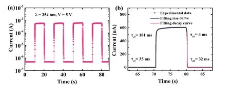
Fig.4.(Color online) (a) The time-dependent photoresponse of the Ga2O3 photodetector with external bias to 254 nm illumination,(b) the experimental data and the fitting curve of rise and decay process.
Fig.5(a) shows the spectral response of theβ-Ga2O3MSM photodetector @-1 V and the peak wavelength is located at~250 nm (4.97 eV),which is close to the bandgap ofβ-Ga2O3.The increased responsivity after 400 nm wavelength may be due to the absorption corresponding to the defect energy level.The rejection ratio (R250nm/R400nm) of 105shows a higher response wavelength selectivity than previously reported results[30,31].Excellent solar-blind ultraviolet detection characteristic demonstrates the high-quality film and strong interband excited transitions.Fig.5(b) gives the responsivities and detectivities of the reported deep ultraviolet photodetectors based on Ga2O3films.It showed clearly that the obtained solar-blind photodetector displays the better comprehensive performance.In addition,the actual responsivity (Ractual) is given byRactual=GRideal=G(ηq/hν)[6],whereηis EQE and ideal responsivity (Rideal) isβ-Ga2O3photodetector detected at 254 nm.Assumingηis 100% andRidealis 0.2 A/W,the gain (G) is equal to 7110 indicating huge internal gain inβ-Ga2O3photodetector.

Fig.5.(Color online) (a) The photocurrent spectrum of β-Ga2O3 MSM detector at -1 V bias in semilog scale,(b) the responsivity vs detectivity of different solar-blind photodetectors[32-41].
4.Conclusion
In summary,a Ga2O3buffer layer is introduced to reduce lattice-mismatch-related defects using MOCVD method.It is found thatTBwill obviously affect crystalline quality and the optimized buffer layer temperature for two step method is 700 °C.The MSM solar-blind photodetector shows ultrahigh responsivity of 1422 A/W and superior detectivity of 2.5× 10¹⁵Jones.Besides,a notable rejection ratio (R250nm/R400nm) of 105is realized,indicating the excellent wavelength selectivity.A remarkable gain of 7110 further demonstrates high internal gain in theβ-Ga2O3MSM photodetector.The outstanding photodetector performance suggests that two-step growth method has great potential for preparing high-qualityβ-Ga2O3film on sapphire.
Acknowledgements
This work was supported by the National Key Research and Development Program of China (Grant No.2020YFB2206103)
杂志排行

Journal of Semiconductors的其它文章
- Efficient flexible dye-sensitized solar cells from rear illumination based on different morphologies of titanium dioxide photoanode
- An advanced theoretical approach to study super-multiperiod superlattices: theory vs experiments
- Controllable step-flow growth of GaN on patterned freestanding substrate
- Controllable thermal rectification design for buildings based on phase change composites
- Enhanced thermal emission from metal-free,fully epitaxial structures with epsilon-near-zero InAs layers
- Research progress of alkaline earth metal iron-based oxides as anodes for lithium-ion batteries