Increasing linear flux range of SQUID amplifier using self-feedback effect
2023-12-02YingYuChen陈滢宇ChaoQunWang王超群YuanXingXu徐元星YueZhao赵越LiLiangYing应利良HangXingXie谢颃星BoGao高波andZhenWang王镇
Ying-Yu Chen(陈滢宇), Chao-Qun Wang(王超群), Yuan-Xing Xu(徐元星), Yue Zhao(赵越),Li-Liang Ying(应利良), Hang-Xing Xie(谢颃星), Bo Gao(高波),†, and Zhen Wang(王镇)
1Shanghai Institute of Microsystem and Information Technology,Chinese Academy of Sciences(CAS),Shanghai 200050,China
2Shanghai Institute of Optics and Fine Mechanics,Chinese Academy of Sciences,Shanghai 201800,China
3CAS Center for Excellence in Superconducting Electronics(CENSE),Shanghai 200050,China
4University of Chinese Academy of Sciences,Beijing 100049,China
Keywords: translation edge sensors,superconducting quantum interference device(SQUID),self-feedback PACS:85.25.Dq,85.25.Oj DOI:10.1088/1674-1056/acd8ac
1.Introduction
Transition edge sensors (TESs) are high-performance energy-resolved photon detectors, which are the key components of the Hot Universe Baryon Surveyor (HUBS), a proposed Chinese space x-ray telescope aiming to search for the so-called “mission baryons”.[1]The detector array of HUBS consists of more than 3600 TES pixels.To read such a large number of low temperature detectors, a multiplexed readout technique is required to reduce the number of cables that connect superconducting quantum interference device (SQUID)amplifiers with room temperature electronics.[2]Otherwise,the thermal loads caused by the cables may exceed the cooling power of the cryo-cooler.A multiplexed readout is also indispensable for a space mission to meet the critical requirements for the weight and power consumption of the readout electronic system.Time-division multiplexing(TDM)is a mature multiplexed readout technique,[3]and it is considered as a candidate readout technique for HUBS.The basic idea of TDM is to connect a certain number of sensor SQUID amplifiers in series and each individual sensor SQUID is coupled with one TES pixel.The signal from each individual TES pixel can be amplified sequentially by activating the sensor SQUIDs one by one, and the multiplexed readout is realized.The number of TES pixels in one readout module is the multiplexing (Mux)factor of the TDM system.[4]The larger this number,the less readout modules are needed.The Mux factorNis constrained by the maximal tolerable readout noise and also by the linear flux range of the sensor SQUID amplifier.The TDM technique suffers a noise penalty because of the enhanced noise bandwidth, which is scaled up linearly with the Mux factor.Therefore, the current noise of the TDM readout is scaled up withN1/2.The TDM usually incorporates a digital flux-locked loop(DFLL)technique.[5]All the sensor SQUIDs in a readout module are initially locked to their own working points.During operation, the error signal (the deviation from the initial locking point)of each sensor SQUID is measured.The error signal is used to calculate the flux feedback signal,which will be used in the next time frame to restore the sensor SQUIDs back to their working points.Proper working of the DFLL circuit should keep the error signal within the linear flux range of the sensor SQUID.[6]The flux variation between two successive readouts of one sensor SQUID needs to be less than its linear flux range,and satisfy the following condition:
whereMinis the mutual inductance of the input coil of the sensor SQUID,trowis the dwell time for each sensor SQUID in one-time frame,Nis the Mux factor, dI/dt(max)is the maximal slew rate of the current signal generated by the TES,LFR is the linear flux range normalized to one flux quantum,andcis a factor referring to the percentage of the linear flux range allocated to the rising edge of the TES current signal.[7]Increasing the flux range raises the upper limit of the Mux factorNand makes a higher mutual inductance feasible,which also conduces to reducing the current noise of the SQUID amplifier.In this paper, we present a method to increase the linear flux range by designing a sensor SQUID with asymmetric loop inductance.Both numerical simulations and the experimental characterizations are conducted.
2.Design of asymmetric SQUID
2.1.Self-feedback effect
A DC SQUID consists of two Josephson junctions embedded in a superconducting loop.The superconducting loop is usually divided into two branches, as schematically shown in Figs.1(a) and 1(b).The inductances of the two branches,denoted asLleftandLright, can be equal or different, depending on where the bias current flows into/out of the superconducting loop.The critical current of the SQUID is tuned by the magnetic flux through the superconducting loop.The total magnetic flux through the SQUID is the sum of the externally applied flux and the flux generated by the current that flows through the SQUID.If the inductance of the left branch and the right branch are equal, the bias current flows symmetrically through both branches and the net magnetic flux produced by the bias current is zero.If the inductancesLleftandLrightare not equal, the current in the left branch and the right branches will be different.Therefore,the bias current of the SQUID will contribute to the total magnetic flux through the SQUID.[8]Inspired by the talk of Irwin,[9]we call this the self-feedback effect,and we study its influence on the SQUID response to an externally applied flux.

2.2.Numerical simulations of SQUID responses
We numerically simulate the response of SQUID to an externally applied flux for the SQUID designs as shown in Figs.1(a) and 1(b).The simulation is a transient analysis in the time domain,and the externally applied flux is realized by a piecewise linear sweep current.Table 1 gives the simulation parameters of both SQUIDs.The parameters are derived from the geometry of the SQUID designs and from the known fabrication process parameters.We simulate the response of current-biased SQUID and voltage-biased SQUID to the externally applied flux.In the voltage-biased case,a bias resistor with a resistance of 0.5 Ω is connected in parallel with the SQUID.[10]We simulate the currents flowing through the left branch and the right branch of the SQUID loop, which vary with externally applied flux.
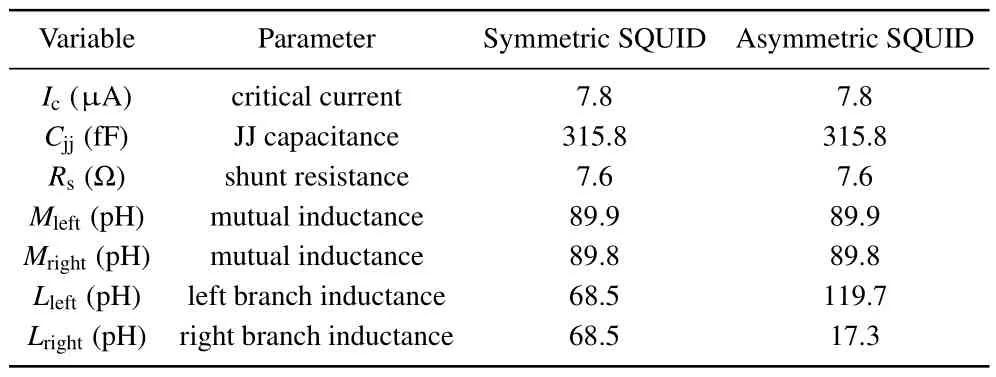
Variable Parameter Symmetric SQUID Asymmetric SQUID Ic (µA) critical current 7.8 7.8 Cjj (fF) JJ capacitance 315.8 315.8 Rs (Ω) shunt resistance 7.6 7.6 Mleft (pH) mutual inductance 89.9 89.9 Mright (pH) mutual inductance 89.8 89.8 Lleft (pH) left branch inductance 68.5 119.7 Lright (pH) right branch inductance 68.5 17.3
Figures 2(a)and 2(b)show the results for current-biased SQUIDs.The bias current is set to 16.2µA,which is slightly greater than 2Ic.For the two SQUID designs, the currents flowing through the left branch (Ileft) and the right branch(Iright) are mirror images of each other, so the total current through the SQUID is a constant.In both cases,theV–Φcurve does not show any asymmetry,and the slopes along the positive and negative sides are equal to each other.The difference in the SQUID design only results in a phase shift in theV–Φcurve.For the symmetric design, the maximum of theV–Φcurve appears atΦ/2,whereas for the asymmetric design,the maximum deviates from that position.
Figures 2(c) and 2(d) show the results for the voltagebiased SQUIDs.The bias current is set to 20.9 µA.Figure 2(c) shows the simulation results for a symmetrically designed SQUID.The branch currentsIleftandIrightare expected to be identical, which is confirmed by the simulation.The slight phase shift is caused by the time delay when the flux bias current flows through two series-connected input inductors, one of which is coupled toLleftand the other is coupled toLright.The total current through the SQUID, which is the sum ofIleftandIright, is also shown by the black dotted line.As seen in the figure,theItotal–Φcurve is symmetric.
We now turn to the SQUID with asymmetric loop inductance.As seen in Fig.2(d), the current flowing through the left branch and the current flowing through the right branch are significantly different from each other.The modulation depth is higher for the current flowing through the branch with lower inductance.TheItotal–Φcurve is asymmetric with the positive slope steeper than the negative slope.

We compare the values of linear flux rangeΦlinof the SQUIDs under voltage bias.The linear flux range depends on the working-point of the SQUID.We usually set the working point on theI–Φcurve where the slope is maximized to obtain an optimal noise performance.In Figs.2(c) and 2(d),theI–Φcurves are approximated by the solid lines.[11]2δIis the usable current swing range and the transfer coefficient at the working point is defined asIΦ=δI/δΦ.The linear flux range is defined as 2δΦ.For the symmetric SQUID design,the transfer coefficient calculated at the chosen working point is 18µA/Φ,and the corresponding linear flux range is 0.23Φ.For the asymmetric SQUID design, the transfer coefficient at the working point is 12 µA/Φ, and the linear flux range is 0.32Φ.The linear flux range is expanded by 45%in the latter case.
2.3.Experimental characterizations
We fabricate the SQUID devices described above by using the standard Nb–(Al–AlOX)–Nb Josephson devices fabrication process developed at the Shanghai Institute of Microsystem and Information Technology.[12]
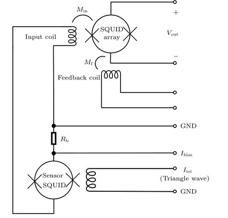
To measure theI–Φcurve of a voltage-biased sensor SQUID, we set up the circuit shown in Fig.3.The sensor SQUID is inductively loaded with the input coil of an SQUID series array (SSA) amplifier.The SSA contains 16 single SQUIDs,and it operates in the flux-locked-loop(FLL)mode and acts as a current-to-voltage amplifier.[13]The transimpedance gain of the SSA is
We use a feedback resistor with a resistance of about 10 kΩ,and the input mutual inductance of the SSA,Min, is approximately equal to the feedback mutual inductanceMrb.The trans-impedance gain of the SSA in the FLL mode is roughly 10 kΩ.A 200-Hz triangular wave signal is applied to the input coil of the sensor SQUID to visualize theI–Φcurve.The amplitude of the triangular wave signal is set to 40 µA.The bias resistance Rb is about 0.5 Ω and the bias current is set to 21µA.
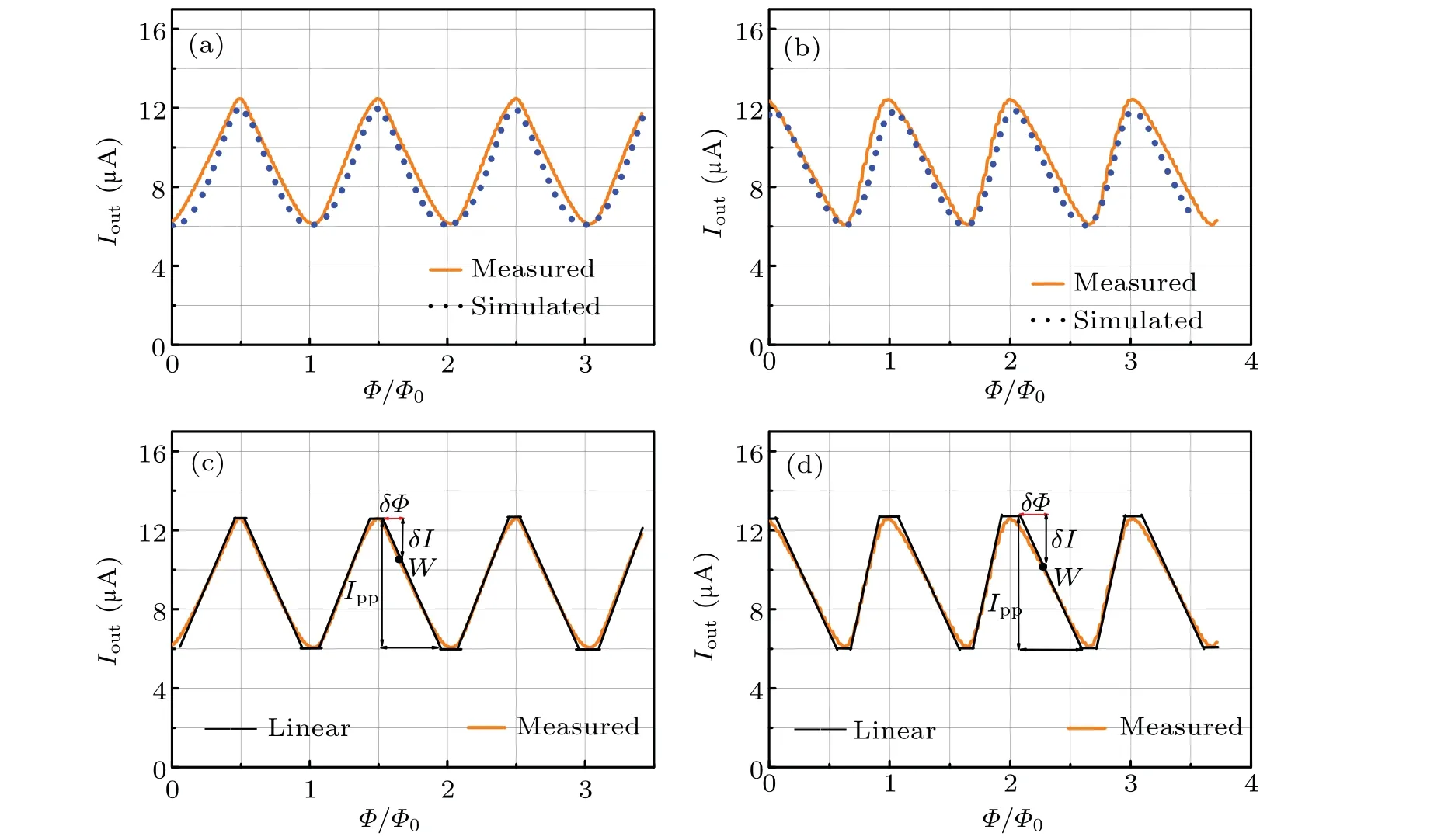
Figures 4(a) and 4(b) show the simulated and measuredI–Φcurves of the symmetric SQUID and asymmetric SQUID.The simulated curves match well with the experimental curves.Figures 4(c) and 4(d) each show the linear flux range deduced from the experimental curve.The transfer coefficient at the working point and the linear flux range for the symmetric SQUID design are 19µA/Φand 0.25Φ;while the corresponding values for the asymmetric SQUID design are 13 µA/Φand 0.36Φ.The experimental results confirm that the asymmetric SQUID design improves the linear flux range.
3.Conclusions
We designed an asymmetric SQUID by putting most of the SQUID loop inductance on one side of the SQUID loop.The self-feedback effect leads to an asymmetricI–Φcurve of the voltage-biased SQUID,which can be seen in the numerical simulations and also confirmed by the experimental measurements.The linear flux range is enhanced along the negative slope side of theI–Φcurve.Sensor SQUIDs that adopt such a design can be used to develop a two-stage TDM readout system for TES array.
Acknowledgements
We thank Dr.Jie Ren for providing SFQ design infrastructure and Mark R.Kurban for drafting this manuscript.
Project supported by the Fund from China National Space Administration (CNSA) (Grant No.D050104) and the Fund for Low Energy Gamma Ray Detection Research Based on SQUID Technique, the Superconducting Electronics Facility(SELF)of Shanghai Institute of Microsystem and Information Technology,Chinese Academy of Sciences.
猜你喜欢
杂志排行

Chinese Physics B的其它文章
- Optimal zero-crossing group selection method of the absolute gravimeter based on improved auto-regressive moving average model
- Deterministic remote preparation of multi-qubit equatorial states through dissipative channels
- Direct measurement of nonlocal quantum states without approximation
- Fast and perfect state transfer in superconducting circuit with tunable coupler
- A discrete Boltzmann model with symmetric velocity discretization for compressible flow
- Dynamic modelling and chaos control for a thin plate oscillator using Bubnov–Galerkin integral method