Etching characteristics and surface modification of InGaSnO thin films under Cl2/Ar plasma
2023-11-16YoungHeeJOOJaeWonCHOIBoHOUHyuckInKWONDooSeungUMandChangIlKIM
Young-Hee JOO, Jae-Won CHOI, Bo HOU, Hyuck-In KWON,Doo-Seung UMand Chang-Il KIM,∗
1 Department of Electronic and Electrical Engineering, Chung-Ang University, Seoul 06974, Republic of Korea
2 Department of Firearms and Optics, Daeduk University, Daejeon 34111, Republic of Korea
Abstract
Keywords: InGaSnO, Cl2-based plasma, etching mechanism, surface modification, plasma etching
1.Introduction
Amorphous oxide semiconductor thin-film transistors (TFTs)have attracted interest for their potential applications in displays and sensors owing to their advantages such as high optical transparency and high on/off current ratio (Ion/Ioff)[1-3].Among the various amorphous oxide semiconductors,amorphous InGaZnO (IGZO) is the most widely used for TFTs because of its high mobility, low leakage current, and scalability for large areas [4-7].Nevertheless, improving mobility and reducing the processing temperature for applications in high-resolution, large-area, and flexible displays and sensors are still necessary[8-10].Recently,a new type of thin film, InGaSnO (IGTO), has been the subject of research owing to its potential for high mobility and low-temperature processing [8, 11].IGTO-based TFTs have demonstrated higher electron mobility in low-temperature processes compared to IGZO-based TFTs [12, 13].This means that IGTObased TFTs can deliver current more efficiently, resulting in higher performance due to faster switching.Additionally,IGTO films have a wider bandgap than IGZO films, making them more suitable for high-performance, high-temperature,and high-power applications such as display backplanes and high-voltage switching devices [14].
To fabricate TFTs, either an etch-stop layer or a backchannel etch process is used.The back-channel etching process is widely used because it uses less photopatterning and can shorten the channel length compared to the etch-stop layer process[15,16].However,when a TFT is manufactured using the back-channel etch method, the channel layer is exposed to plasma during the patterning process of the source and drain electrodes[15,17].Because the plasma process can affect the performance or reliability of TFTs, it is a critical consideration when fabricating TFTs[18-20].However,there are few studies on the plasma-etching characteristics of IGTO thin films and changes in thin-film characteristics after etching.
In this study, we investigated the etching characteristics of IGTO thin films using plasma and observed the changes in their surface characteristics before and after the etching process under Cl2/Ar plasma.The plasma-etching tendency was evaluated according to various variables such as the Cl2/Ar gas-mixing ratio, upper radio-frequency (RF) power, bottom RF power, and process pressure.X-ray photoelectron spectroscopy(XPS)analysis was performed to understand the etching mechanism and confirm changes in the surface state,such as the residue on the surface after etching,and ultraviolet photoelectron spectroscopy (UPS) analysis was performed to confirm the change in work function accordingly.Further,changes in surface roughness and wettability according to the etching process were analyzed through atomic force microscopy (AFM) and a contact angle analyzer.
2.Experiment
Figure 1 shows a structural diagram of a high-density plasma (HDP) system for the etching process.This system uses a combined plasma source with inductively coupled plasma coil and capacitively coupled plasma flat electrodes.A source electrode above the main chamber is connected to a 13.56 MHz RF generator to induce an HDP.The electrode for bias voltage located at the bottom is connected to a 2 MHz RF generator to control the energy of ions moving from the plasma to the substrate.
The IGTO thin film was etched under Cl2-based plasma,and the standard etching conditions were fixed as follows:gas flow rate of 100 sccm,source power of 500 W,bias power of 100 W, and process pressure of 15 mTorr.
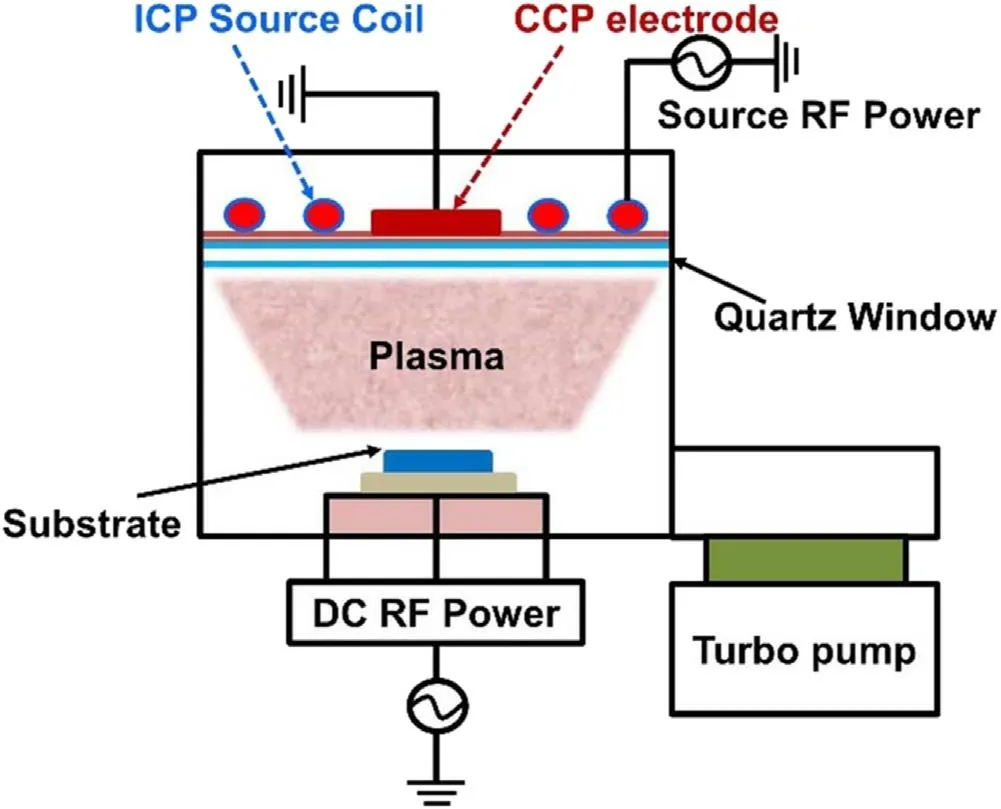
Figure 1.Structural diagram of the high-density plasma system with a combined plasma source.

Figure 2.Etch rate of the IGTO thin film and selectivity to photoresist (PR) and Al depending on the Cl2/Ar gas flow rate.

Table 1.Melting and boiling points of expected etch by-products of the IGTO thin film under Cl2 plasma.
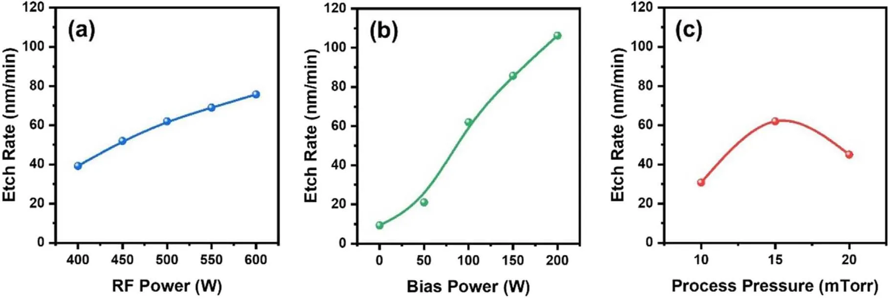
Figure 3.Effects of process input parameters on etch rate: (a) upper RF power, (b) bottom RF power, and (c) process pressure.
The etch rate was measured using a surface profiler(Alpha-step 500, Tencor).After the etching process, XPS(NEXSA,Thermo-Fisher Scientific)analysis was performed to elucidate the etching mechanism by confirming the chemical bonding state of the surface of the IGTO thin film, and UPS(NEXSA,Thermo-Fisher Scientific)analysis was performed to measure the variation of work function.Additionally,an AFM(NX-10, Park system) and a contact angle analyzer (Phoenix 300,SEO)were employed to investigate the changes in surface roughness and surface energy before and after etching.
3.Results and discussion
The process was performed using Cl2/Ar plasma to evaluate the etch rate of the IGTO thin film.The total gas flow rate was 100 sccm, with a source power of 500 W, bias voltage of 100 W, and process pressure of 15 mTorr being maintained.Figure 2 shows the etch rate of the IGTO thin film and the selectivity to PR and Al according to the flow rate of Cl2in Cl2/Ar mixed gas.Figure 2 reveals that as the flow rate of Cl2increases from 0 to 100 sccm, the etch rate of the IGTO thin film increases from 9 to 69 nm min−1.This result indicates that the chemical reaction with Cl or Cl2radicals rather than the physical reaction with Ar ions is the primary etching mechanism in the etching of the IGTO thin film [21, 22].When the IGTO thin film is etched using Cl2/Ar mixed gas,the by-products generated on the surface of the IGTO thin film are a combination of Cl and metals such as InClx,GaClx,and SnClx.These by-products are easily removed from the surface of the thin film owing to its low boiling point[23,24].Therefore,as the flow rate of Cl2increases,the etch rate of the IGTO thin film increases.Table 1 lists the boiling and melting points of the by-products.The etching selectivities to PR and Al were the highest at 0.31 and 0.75, respectively, under the pure Ar plasma condition.This is considered to be because PR and Al films also scarcely react with Ar plasma.When Cl2gas was added,the selectivity dropped drastically to 0.02 and 0.065.Then,the selectivity gradually increased as the amount of Cl2gas increased.
Figure 3 shows the etch rate of an IGTO thin film depending on various process parameters such as upper RF power, bottom RF power, and process pressure.When the upper RF power was increased, the etch rate of the IGTO thin film also increased continuously from 39.25 to 75.75 nm min−1.Increasing the upper RF power increases the density of Cl radicals in the plasma, which means more radicals can reach the IGTO thin film,thereby increasing the chemical reaction with the thin film [25, 26].Figure 3(b)shows the correlation between the bottom RF power and the etch rate of the IGTO thin film, which was measured by increasing the bias power from 0 to 200 W while keeping the Cl2/Ar ratio at 100/0(sccm/sccm),RF power at 500 W,and process pressure at 15 mTorr.The etch rate was found to rapidly increase with the bottom RF power and reached its highest value of 106.25 nm min−1at a bottom RF power of 200 W.In Cl2plasma,the Cl2molecules are dissociated into Cl radicals and Cl+ions.The Cl+ions are positively charged and can be attracted to the substrate negatively charged by the bottom RF power, where they can chemically react with and bombard the IGTO surface [27, 28].In addition,increasing the RF bias power increase the amplitude of the oscillating electric field and can lead to a higher self-bias voltage, resulting in an improved etch rate [29].The combination of these effects can cause a rapid increase in the etch rate.Figure 3(c) presents the correlation between process pressure and etch rate.The etch rate was evaluated by varying the process pressure from 10 to 20 mTorr while maintaining the Cl2/Ar flow rate at 100/0(sccm/sccm),RF power at 500 W, and bias power at 100 W.The results revealed an increase in the etch rate with increasing pressure up to a maximum value of 62 nm min−1at a process pressure of 10 mTorr, followed by a decrease at higher pressures.At extremely low pressures, the etch rate is limited owing to a reduced concentration of ions and radicals in the plasma,which results in limited surface reaction.At certain intermediate pressures, the plasma is dominated by high-energy ions and radicals that can cause significant physical and chemical damage to the substrate surface, leading to high etch rates.However, at high pressures, ion and radical species as well as gas molecules undergo frequent collisions with each other and with the chamber walls, resulting in a shortened mean free path and reduction in collision energy and reactivity [30, 31].This can lead to a reduction in the etch rate owing to reduced surface reaction between the species and the substrate, as the ion and radical species become less energetic and less likely to react with the substrate.
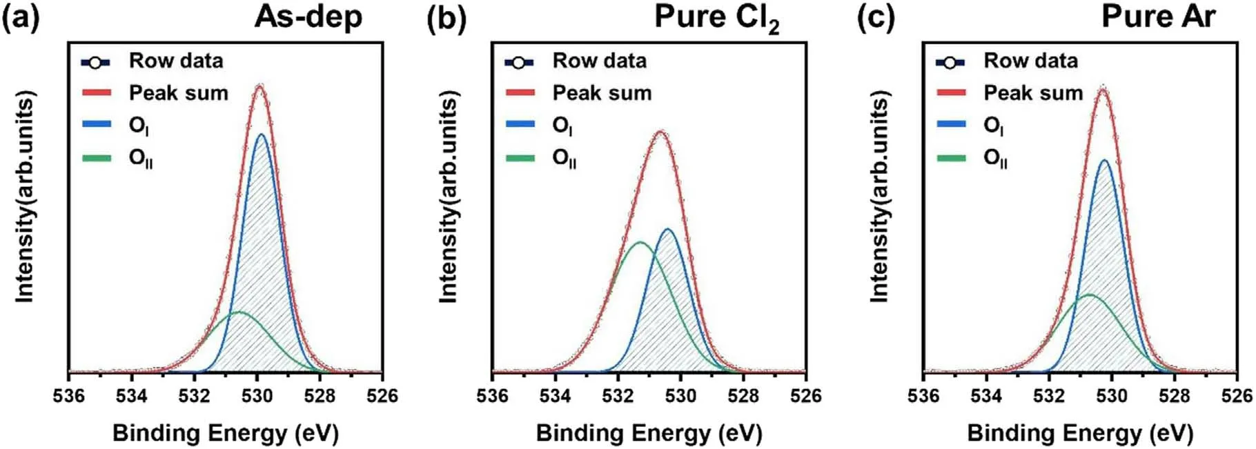
Figure 4.O 1s x-ray photoelectron spectroscopy(XPS)spectra with fitting results.(a)As-deposited,(b)pure Cl2,(c)pure Ar.The ranges of the x and y axes are the same for all data.

Figure 5.XPS spectra according to Cl2/Ar gas flow.(a) In 3d, (b) Ga 2p, and (c) Sn 3d.
XPS analysis was conducted to investigate the etching mechanism of IGTO thin films on their surface.Figure 4(a)shows the O 1s peak of the IGTO thin film before etching,while figures 4(b) and (c) show the O 1s peak of the IGTO thin film after etching in Cl2and Ar plasmas, respectively,under standard etching conditions.The raw data of the O 1s peak were deconvoluted into two components, OIand OII,which represent the metal-oxygen bond and oxygen-deficient and O-H bonds, respectively [32, 33].Upon etching with pure Cl2plasma, the OIpeak decreased in comparison to the pre-etched state, as observed in figure 4(b).This indicates that Cl or Cl2radicals and ions react with the metals in IGTO films to generate volatile by-products such as InClx,GaClx,and SnClx,leading to etching.Additionally,the OIIpeak increased, as the Cl radicals combined with oxygen (Clx-Oy) and were volatilized.By contrast, the O 1s peak did not significantly change upon etching with pure Ar plasma as shown in figure 4(c).The OIpeak was reduced and OIIpeak slightly increased compared to the pre-etched state,indicating that the oxygen atoms in metal oxide bonds are removed as the bond is broken because of the influence of Ar ion sputtering.However,the peak change of OIand OIIis quite insignificant compared to the etching result in Cl2plasma.Thus,chemical reactions have a greater effect on the etching of IGTO thin films than the physical sputtering of Ar ions.Overall, the results suggest that the etching of IGTO thin films under Cl2/Ar mixed gas is primarily driven by chemical reactions.In particular, the Cl-based radicals and ions combine with the metal and oxygen to induce etching,as highlighted in figure 2.
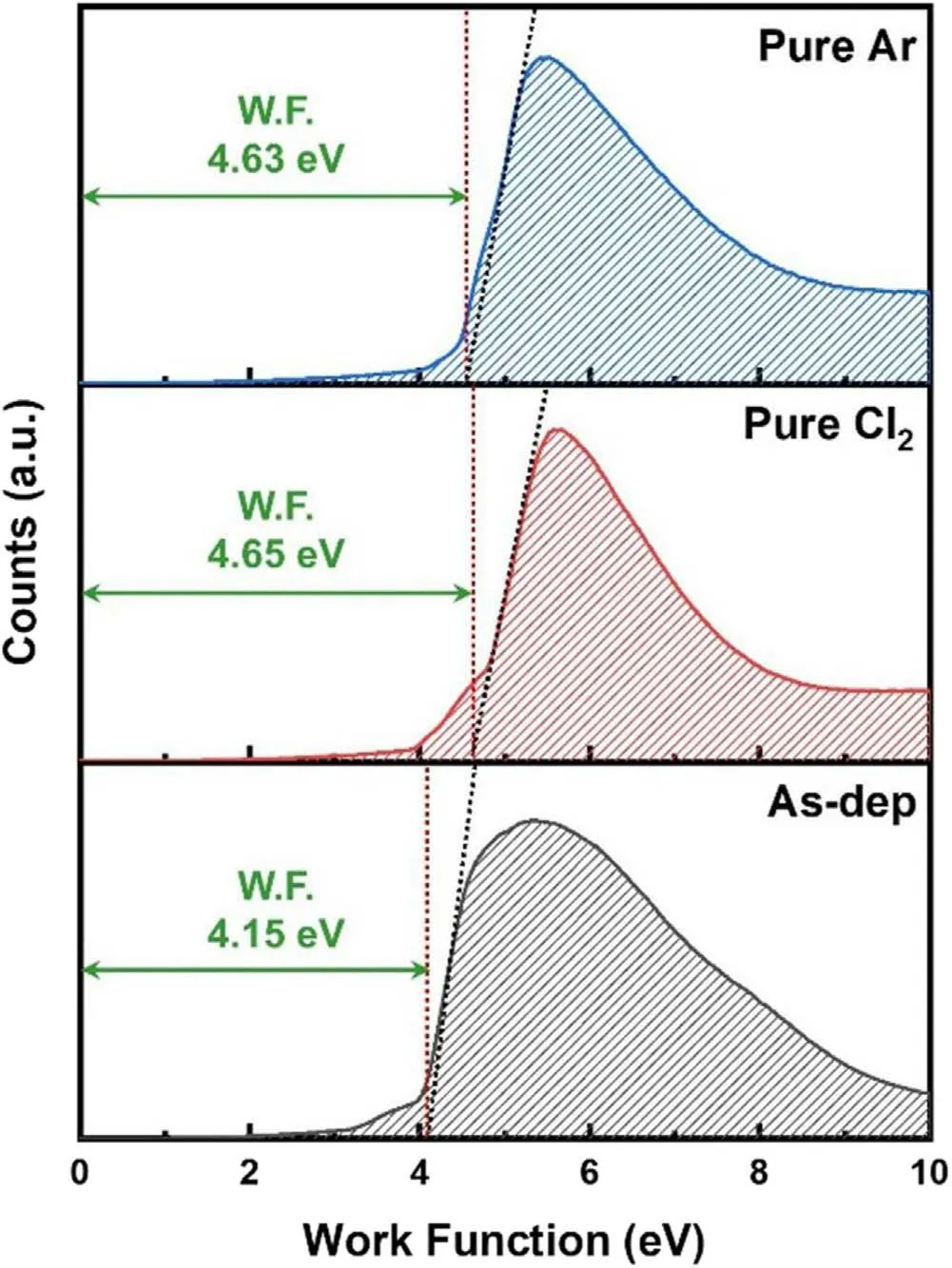
Figure 6.Work function of the IGTO thin film according to Cl2/Ar gas flow.
Figure 5 shows the peak shift and differences in In 3d,Ga 2p, and Sn 3d spectra before and after the Cl2plasma etching as well as after the Ar plasma etching.The largest shift in all three spectra (In 3d, Ga 2p, and Sn 3d) occurred after etching in pure Cl2plasma.In 3d exhibited a shift to a higher binding energy of ∼0.5 eV for pure Cl2and ∼0.3 eV for pure Ar plasma.Similarly, Ga 2p shifted to a higher binding energy of ∼0.6 eV for pure Cl2and ∼0.4 eV for pure Ar.Further,Sn 3d shifted to a higher binding energy of∼0.5 eV for Cl2and ∼0.3 eV for pure Ar.Peak shifts in XPS spectra indicate changes in the binding energy of the emitted electrons, which may occur when the element is in a different chemical or structural state than the initial state.The XPS peak shift of the thin film surface etched in pure Cl plasma was higher than that of the sample etched in pure Ar plasma, possibly because Cl-based radicals and ions combined with the metals (In, Ga, and Sn) during the etching process, with some remaining as residues.This is expected to result in a larger peak shift.
The surface composition of the IGTO thin film was changed by the plasma process used during etching,as shown in figures 4 and 5.A change in the surface composition of the thin film changes the various physical properties of the thin film, e.g.the work function, which is an essential parameter in the design of devices and systems.Therefore, the change in the work function of the IGTO thin film according to the type of etching gas was investigated.Figure 6 shows the difference in the work function of the IGTO thin film according to the Cl and Ar plasma etching determined by UPS analysis.The work function was calculated using the following formula
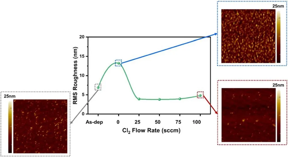
Figure 7.RMS roughness of IGTO thin films according to the gasmixing ratio.
where ∅is the work function and hv is the photon energy equal to 21.2 eV, which is the wavelength of the ultraviolet source.Ecutoffand EFare the cutoff energy and Fermi level energy, respectively.
针对式(19),采用经验风险最小化(Empirical Risk Minimization,ERM)[23]来获得差分隐私处理的最优pu,即
The corresponding work function of the as-deposited IGTO thin film was 4.19 eV.The work functions of the IGTO thin film increased to 4.65 and 4.63 eV after pure Cl and pure Ar plasma etching,respectively.Although significant changes in the work function were observed before and after etching,a difference of only ∼0.02 eV could be observed under different plasmas.This could be attributed to the fact that the plasma-etching process causes defects on the surface of the thin film,and the presence of these defects increases the energy required to capture electrons and remove them from the surface [34, 35].
In figure 7,the surface roughness of the IGTO thin film is shown as a function of the Cl2/Ar gas ratio.The as-deposited IGTO thin film had a surface roughness of 6.91 nm, which significantly increased to 13.23 nm after etching in pure Ar plasma.However, when Cl2gas was introduced, the surface roughness immediately decreased to 3.92 nm.This is attributed to the excessive physical collisions between Ar ions and the thin-film surface,which resulted in surface roughening.As Cl2gas is added, the physical energy of the plasma decreases,while the chemical reaction between Cl-based radicals and ions and the surface of the IGTO thin film increases.Consequently, the surface roughness decreases owing to the formation of a more uniform and smoother surface.
4.Conclusion
In conclusion, we investigated the etching characteristics of IGTO thin films using Cl2/Ar plasma and analyzed the changes in surface properties before and after etching.The results indicated that the etch rate of the IGTO thin films increased with an increase in the ratio of Cl2in the Cl2/Ar mixture gas, with the highest etch rate observed at 69 nm min−1in pure Cl2plasma with a gas flow rate of 100 sccm.Additionally, an increase in upper and bottom RF power led to an increase in the etch rate, and a process pressure of 15 mTorr was optimal.From etch rate measurements and XPS surface analysis, we could conclude that the primary etching mechanism for IGTO thin films under Cl2plasma is a chemical reaction, and a significantly increased work function indicates the occurrence of defects on the surface.The etching process reduced surface roughness in Cl2-containing plasma,whereas the etching process in pure Ar plasma increased surface roughness.This indicates that etching conditions significantly affect the surface properties of IGTO thin films.
Overall, our results provide important data for the practical application of IGTO thin films in TFT devices.As there are limited studies on the plasma-etching characteristics of IGTO thin films and changes in their properties after etching,these results offer valuable insights for various IGTO-based applications.
Acknowledgments
This research was supported by the Chung-Ang University Research Grants in 2021 and the National Research Foundation (NRF) of Korea (No.2020R1G1A1102692).
Author contributions
Young-Hee Joo:Conceptualization, Methodology, Investigation, Data Curation, Visualization, Writing - original draft;Jae-Won Choi:Investigation, Data Curation;Bo Hou:Data Curation, Writing - review and editing;Hyuck-In Kwon:Conceptualization, Methodology;Doo-Seung Um:Conceptualization, Validation,Resources, Visualization, Writing -review and editing,Supervision,Funding acquisition;Chang-Il Kim:Conceptualization, Writing - review and editing,Supervision, Project administration, Funding acquisition.
猜你喜欢
杂志排行

Plasma Science and Technology的其它文章
- A laser-produced plasma source based on thin-film Gd targets for next-generation extreme ultraviolet lithography
- The effect of pulse voltage rise rate on the polypropylene surface hydrophilic modification by ns pulsed nitrogen DBD
- Comparative study on the degradation of phenol by a high-voltage pulsed discharge above a liquid surface and under a liquid surface
- Room-temperature degradation of o-xylene in simulated air using an online-regenerable plasma-catalysis reactor with low amounts of nanosized noble metals on Co3O4
- Enhanced surface-insulating performance of EP composites by doping plasmafluorinated ZnO nanofiller
- Endurance-test and theoretical prediction of a rare earth nanocathode for the applied field magnetoplasmadynamic thruster