A homogeneous atmospheric pressure air plasma in a 10mm gap based on a threeelectrode configuration
2023-11-16ZhiyuLI李志宇DaweiLIU刘大伟XinpeiLU卢新培andLanlanNIE聂兰兰
Zhiyu LI (李志宇), Dawei LIU (刘大伟), Xinpei LU (卢新培)and Lanlan NIE (聂兰兰)
State Key Laboratory of Advanced Electromagnetic Engineering and Technology,School of Electrical and Electronic Engineering, Huazhong University of Science and Technology, Wuhan 430074, People’s Republic of China
Abstract
Keywords: atmospheric pressure plasma, homogeneous discharge, glow discharge, air plasma
1.Introduction
Atmospheric pressure nonequilibrium plasma (APNP) has attracted a lot of attention in recent years.Because it can generate a variety of reactive species at a low gas temperature,APNP has broad prospects in various applications, including surface treatment, pollution control, sterilization, plasma medicine, and so on [1-14].
Dielectric barrier discharge (DBD), first reported by Siemens in 1857 [15], remains one of the most widely used configurations to generate APNP.When noble gas is used, it is easy to generate homogeneous APNP in a relatively large gap.However, when the working gas is air, the plasma appears homogeneous only when the gap distance is shorter than 4 mm[16, 17].Otherwise, it always appears filamentary even when nanosecond pulsed direct current (DC) voltage is used.From an application point of view, such as surface modification, it is desirable to generate homogeneous APNP to achieve a uniform plasma treatment effect.
To date, a lot of effort has been made to generate homogeneous DBD in air, such as using different dielectric materials [18-20], pulsed power supply with different pulse rising times [16, 21-24] and different repetition frequencies[16, 23, 24], and so on.
In our previous work, we found that in the configuration of non-equal gap DBDs [25, 26], the plasma would be distributed in a stripe shape or a ladder shape, rather than randomly distributed on the surface of the dielectric layer, so that the uniform plasma treatment effect could be achieved by scanning the plasma over the surface.
But in general, a diffuse discharge can be obtained only when the air gap distance is less than 4 mm, otherwise, the discharge will transit to filamentary mode[17,27,28].Wang et al [29] calculated the variation of the head electric field with the length of electron avalanche during the development of electron avalanche.It was concluded that when the length is larger than 5 mm, the ratio of the space charge field to the applied electric field is approximately equal to 1, which is considered the criterion for an electron avalanche to transit to a streamer [30, 31], indicating that if the air gap distance exceeds 5 mm, the discharge will always transit to filamentary mode.
Recently, researchers have reported that homogeneous air DBDs are generated in a gap larger than 4 mm.Qi et al[32] reported that a homogeneous air DBD is generated in a 7 mm gap driven by a short pulse voltage with a rising time of 4 ns.The plasma is generated in the whole gap homogeneous in both horizontal and longitudinal dimensions.But its gas temperature is estimated to be as high as 1300 K, which is much higher than room temperature.Liu et al[33]proposed a line-plate electrode with a parallel floating electrode.The discharge at the contact point between the HV electrode and the floating electrode can improve the uniformity of discharge in the gap.But the plasma is only generated within a narrow strip area, similar to a ‘curtain’.
In this paper,we propose a DBD device based on a threeelectrode configuration, i.e., the two electrodes form the surface dielectric barrier discharge (S-DBD), and together with the third ground electrode generate homogeneous volume APNP in an air gap up to 10 mm.The surface DBD can generate a high concentration of electrons, ions, metastable, and excited species, which is favorable for the generation of homogeneous volume plasma in the main discharge gap.It has also been found that the gas temperature of the discharge is close to room temperature,and could improve the hydrophilicity of the surface of a variety of polymer materials.
2.Experimental setup
The DBD device is composed of three electrodes as shown in figure 1(a).Two of the electrodes are composed of multiple pairs of parallel strip electrodes embedded in a dielectric plate(dielectric constant ε ≈4.2), forming an S-DBD configuration.As shown in figure 1(b), the electrode connected to a sinusoidal HV AC power supply is called the HV electrode and the electrode grounded through a resistor is called the middle electrode.Even if there is no ground electrode (the third electrode), plasma can also be generated in a region of 40×5 mm2on the surface of the dielectric plate.The widths of the strip electrodes are l1=0.6 mm for the middle electrode and l2=0.4 mm for the HV electrode respectively,and the distance between the two electrodes is l3=0.2 mm.The thickness of the dielectric layer between the HV electrode and the surface of the plate is l0=0.12 mm.As for the third electrode, a copper foil on the back of a 1 mm thick alumina ceramic plate(dielectric constant ε ≈9.8)is placed parallel to the dielectric plate embedded with two electrodes, and it is called the ground electrode.The gap distance d between the HV electrode and the ground electrode can be adjusted, and plasma could be generated in the whole air gap.

Figure 1.(a) Schematic of the experimental setup, (b) side view of the experimental setup,(c)schematic of the DBD device without the middle electrode.l0=0.12 mm, l1=0.6 mm, l2=0.4 mm,l3=0.2 mm.
3.Experimental results
First, we investigate the appearance of plasma with resistors of R=500 kΩ and 5 MΩ, which will affect the voltage potential of the middle electrode.Photographs of the plasma under the conditions of different frequencies, different series resistors, and gap distances were captured using a digital camera (Nikon D7500) and are shown in figure 2.When the gap distance is small,such as d=4 mm for R=500 kΩ and d=6 mm for R=5 MΩ,the applied voltage is adjusted to a relatively low value (7.2 kV for d=4 mm and R=500 kΩ,and 13.5 kV for d=6 mm and R=5 MΩ)to avoid the direct breakdown between the HV electrode and the ground electrode.

Figure 2.Photographs of the air discharge of different gap distances under different experimental conditions.(a)Series resistor R=500 kΩ,frequency f=10 kHz, (b) R=5 MΩ, f=10 kHz, (c) R=5 MΩ, f=40 kHz.The applied voltage Ua=7.2 kV for d=4 mm in (a) and 8 kV for the rest in(a).The applied voltage is 13.5 kV for d=6 mm in(b)and(c)and 15 kV for the rest in(b)and(c).The exposure time is 0.75 s.
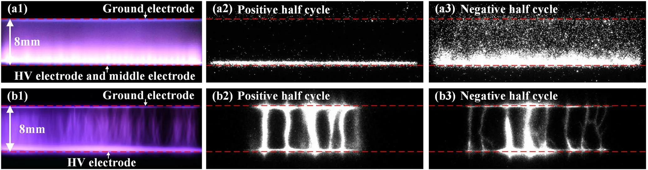
Figure 3.(a1)-(a3)are photographs of the plasma obtained from the device shown in figure 2(a)(with a middle electrode),and(b1)-(b3)are photographs of the plasma obtained from the device shown in figure 2(c)(without a middle electrode).(a1)and(b1)are photographs taken with the digital camera while(a2),(a3),(b2),and(b3)are the photographs taken by an ICCD camera.(a2)and(b2)are captured during the positive half cycle while(a3)and(b3)are captured during the negative half cycle.For both cases,Ua=15 kV,R=5 MΩ,f=10 kHz,and d=8 mm.The exposure time of the ICCD camera is 50 μs.
It can be observed in figure 2(a) that for the case of R=500 kΩ, the brightest region is within the range of less than 1 mm from the bottom dielectric plate,where the S-DBD between the HV electrode and the middle electrode is.The air gap can be completely broken down and the plasma is homogeneous when d=4 mm.Furthermore, with the increase of the gap distance, the plasma in the main air gap still appears diffuse at a gap distance of d=8 mm and it is like a corona discharge at a gap distance of d=12 mm.
For the case of R=5 MΩ,as shown in figure 2(b),when d=6, 8, and 10 mm, the whole air gap is broken down and diffuse plasma can be obtained.Moreover,the plasmas appear with two regions with different brightnesses.The region within the range of about 2 mm from the bottom dielectric plate surface is brighter than the rest of the space.With a further increase in the gap distance to 12 mm,only the surface discharge between the HV electrodes and the middle electrodes can be observed and there is no plasma in the main part of the gap.When the frequency of the applied voltage is increased to 40 kHz, as shown in figure 2(c), it is similar to that at 10 kHz.But when the gap distance is 12 mm,the bright region is more than half of the gap.
In order to determine whether the homogeneous plasma generated in the large air gap is due to the S-DBD, another DBD device with only the HV electrode and ground electrode as shown in figure 1(c)is also investigated.As can be seen in figure 3(b1), for the 8 mm gap, there are numerous filamentary discharges between the two parallel plate electrodes.In other words, the plasma is not homogeneous.On the other hand, for the case with the middle electrode, as shown in figure 3(a1), the plasma looks homogeneous.

Figure 4.Temporal evolution of plasma with an ICCD camera exposure time of 100 ns.The discharge parameters are the same as those shown in the photograph in figure 2(b) (Ua=15 kV, R=5 MΩ, f=10 kHz, d=8 mm).
To further confirm whether the plasma is actually homogeneous, an ICCD camera (Andor, DH334T) is used to take photographs of a single discharge.The exposure time of the ICCD camera is set to 50 μs,which is equal to the time of half a cycle of the applied AC voltage.A two-channel pulse signal generator (Tektronix, AFG3102C) is used to synchronize the ICCD camera with the applied voltage to capture the discharge during the positive or negative half cycle.
As shown in figure 3(a2), for the discharge with the middle electrode,during the positive half cycle of the applied voltage, only the discharge on the surface of the bottom dielectric plate can be observed.On the other hand, during the negative half cycle,as shown in figure 3(a3),a homogeneous plasma can be observed in the whole gap while the plasma next to the bottom dielectric plate is brighter.In addition,when R is changed to 500 kΩ,the plasma looks similar.Thus,we can conclude that the plasma with the middle electrode is homogeneous.
However, for the case without the middle electrode, as shown in figures 3(b2) and (b3), during the positive or negative half cycle, there are always multiple discharge filaments throughout the whole gap.Therefore, the surface discharge between the HV electrode and the middle electrode plays an important role in the generation of homogeneous plasma in a relatively large air gap.
Figure 4 shows the temporal evolution of the discharge captured by the high-speed ICCD camera.During the time of 0-50 μs, which is the positive half cycle, plasma only exists on the surface of the dielectric plate embedded with the HV electrode and the middle electrode as mentioned above.During the negative half cycle, first, the surface discharge between the HV electrode and the middle electrode starts at about 60 μs and appears with strong light emission within 3 mm from the surface of the bottom plate at about 63.5 μs.At this stage, there is no volume discharge in the main gap.Second,starting at 69 μs,the volume discharge is ignited and fills the whole discharge gap at 71 μs.Finally,at about 80 μs,the discharge extinguishes.As can be seen from these photographs,there is no filament,which further confirms that the device can generate homogeneous plasma.
Optical emission spectrum (OES) is a useful tool to identify the reactive species in plasma and estimate the rotational temperature and vibrational temperature from the spectra of the N2(C3Πu-B3Πg) (Δv=−2).The OES of the plasma generated in the air gap is measured by a halfmeter spectrometer (Princeton Instruments, Acton SpectraHub 2500i) with a grating of 1200 g·mm−1.The entrance and exit slits of the spectrometer are fixed at 100 μm,and the integration time and the resolution are 500 ms and 0.3 nm,respectively.In order to obtain the optical emission from the main discharge region, the emission from the bottom dielectric plate and the region within 3 mm above the surface are shielded.The emission in the gap is focused by a convex lens into the entrance slit of the spectrometer.The OES of the homogeneous discharge in the three-electrode configuration when R=5 MΩ,Ua=15 kV,f=10 kHz,and d=8 mm is shown in figure 5(a).In the spectrum, N2(C-B) emission in the wavelength range of 300-400 nm,emission at 391.4 nm and 427 nm, and OH emission at 309 nm can be clearly measured.In the range of 500-800 nm, no significant emission line is measured.The optical emission spectra in the range of 200-800 nm for the case of R=500 kΩ are similar to those for the case of R=5 MΩ.
In addition, the N2(C-B) (Δv=−2) experimental spectra are always used to estimate the rotational temperature,which is considered to be equal to gas temperature and crucial to the application, and the vibrational temperature of plasma.Therefore, figure 5(b) shows the N2(C-B) (Δv=−2)experimental spectra of the discharge when R=5 MΩ and 500 kΩ,respectively,measured using a 3600 g·mm−1grating and the simulated spectra obtained from the SPECAIR software.The rotational temperature and the vibrational temperature can be obtained when two spectra achieve best fit.The plasma rotational temperature is about 320 K, which is close to room temperature, and the vibrational temperature of the best fit is 2600 K in the case of R=5 MΩ and 4000 K in the case of R=500 kΩ, respectively.
Finally, the treatment effect of the homogeneous plasma on the surface of polymers is also investigated.Three different kinds of polymers, polytetrafluoroethylene (PTFE),polyvinyl chloride (PVC), and acrylic (PMMA), are placed near the ground electrode in the gap and treated by the homogeneous plasma.Figures 6(a)-(c) show photographs of a 5 μl water droplet on the untreated PVC boards and the PVC board treated by plasma for 1 and 3 min, respectively.Droplets on the untreated PVC surface are hemispherical indicating that the material is hydrophobic and the hydrophilicity of the surface is improved obviously after plasma treatment.Figure 6(d) shows the water contact angle of three different materials treated by the plasma for 3 min while the series resistor of the middle electrode is 500 kΩ or 5 MΩ,respectively.It is interesting to find that the treatment effect of the homogeneous discharge when R=5 MΩ is better than the case when R=500 kΩ.In addition, after the plasma treatment, no obvious damage can be observed on the polymer surface and there is no significant difference in appearance from that of the untreated material.
4.Discussion
As can be seen from the results presented above, the S-DBD plays an important role in the generation of homogeneous APNP in an air gap up to 10 mm.Under the same gap distance,when there is no coplanar surface discharge(no middle electrode), there are numerous filaments in the gap.Schmidt et al [34] reported a similar configuration consisting of a plasma electrode, a metal extraction electrode, and a gap between two parallel plate electrodes, where a corona discharge is generated to induce ionic wind rather than volume plasma [34-36].

Figure 6.Photographs of water droplets on the PVC surface for (a)untreated, and treated by homogeneous air APNP for (b) 1 min and(c)3 min,respectively for R=5 MΩ.(d)Water contact angle of the surface of three different materials after 3 min of plasma treatment.The mean value and the error bar are obtained by repeating the experiment at least three times.The plasma parameters are Ua=15 kV, f=10 kHz, d=8 mm for R=5 MΩ, and Ua=8 kV, f=10 kHz, d=6 mm for R=500 kΩ.
For the three-electrode configuration, during the positive half cycle of the applied voltage, the electrons generated by the surface discharge move to the dielectric plate where the HV electrode is embedded, so there is no electron left in the main gap.In the meantime, the positive ions cannot move to the cathode within a half-cycle period due to their heavy mass.Therefore, there is no discharge in the main discharge gap during the positive half cycle of the applied voltage.
On the other hand,during the negative half cycle,because the middle electrode is also embedded in the dielectric plate,and the distance between the HV electrode and the middle electrode is much shorter than the main discharge gap between two parallel plates,a discharge is first ignited between the HV electrode and the middle electrode at a relatively low voltage.With the increase in the voltage, when enough electrons are deposited on the surface during the discharge between the HV electrode and the middle electrode, the electrons deposited on the bottom dielectric plate along with the applied voltage will generate a driving force, which will result in the electrons moving to the ground electrode through the whole gap.Thus,there will be a high concentration of electrons left in the main gap because of the S-DBD, which is favorable for the generation of homogeneous APNP.
It is generally accepted that the rapid growth of electron avalanches is the reason for the formation of filamentary discharge[30,31].As we know that the ionization coefficient α, which is related to the applied electric field E and the pressure p, directly determines the growth of the electron avalanche.Qi et al reported that the 7 mm air discharge transits from filamentary mode to homogeneous mode only when the gas temperature is increased to 1300 K after about 1 min of discharge [32].This is because with the increase in gas temperature, the molecular number density is decreased and thus the electron mean-free path is increased,which leads to the suppression of electron avalanche.
However, the plasma gas temperature reported in this paper is close to room temperature; thus, the homogeneous plasma in the large air gap is not caused by gas heating.As discussed above,the S-DBD results in a high concentration of seed electrons in the main discharge gap, and there are much more seed electrons than in the case of a two-electrode discharge configuration.These seed electrons move toward the anode,gain energy from the applied electric field,and collide with the gas molecules forming the electron avalanche.Under such conditions,even if in a relatively weak electric field and the ionization coefficient α is relatively small, a sufficient number of electrons can still reach the anode so that the whole gap can be broken down.In addition, in the three-electrode configuration, some long-lived metastable particles generated by the surface discharge may also be helpful to generate the seed electrons and thus reduce the electric field required for discharge.
For the configuration in the experiment,the capacitances of the gap (Cg) and the dielectric layer (Cd) are estimated to be about 0.22 and 13.53 pF, respectively.Therefore, the maximum value of the voltage across the air gap Ugis estimated to be about 14.76 kV, and the electric field applied on the 8 mm air gap is about 18.45 kV·cm−1, which is much lower than the typical breakdown electric field of 30 kV·cm−1for atmospheric pressure air discharge.Therefore, the discharge occurs in an electric field that is significantly lower than the critical breakdown electric field, and it is the main reason for the formation of the homogeneous plasma.
5.Conclusion
In this paper,a homogeneous atmospheric pressure air plasma is reported with a gap distance up to 10 mm, which is based on a three-electrode configuration where a coplanar surface DBD serves as a source of seed electrons.The effect of the gap distance, the series resistor connected to the middle electrode, the dynamics of discharge, and the OES are also studied.During the negative half cycle of applied voltage,high concentrations of electrons are pushed toward the anode,which results in the low breakdown electric field,which is the main reason the homogeneous plasma is obtained.
Importantly,the plasma gas temperature is close to room temperature, which means that it can be used in many applications, such as plasma medicine and material modification, which are sensitive to gas temperature.Surface treatment experiment results show that homogeneous plasma can effectively improve the surface hydrophilicity of a variety of polymer materials.
Acknowledgments
This work is supported by National Natural Science Foundation of China (Nos.52130701, 51977096, 52277150, and 12005076) and the National Key Research and Development Program of China (No.2021YFE0114700).
猜你喜欢
杂志排行

Plasma Science and Technology的其它文章
- A laser-produced plasma source based on thin-film Gd targets for next-generation extreme ultraviolet lithography
- The effect of pulse voltage rise rate on the polypropylene surface hydrophilic modification by ns pulsed nitrogen DBD
- Comparative study on the degradation of phenol by a high-voltage pulsed discharge above a liquid surface and under a liquid surface
- Room-temperature degradation of o-xylene in simulated air using an online-regenerable plasma-catalysis reactor with low amounts of nanosized noble metals on Co3O4
- Enhanced surface-insulating performance of EP composites by doping plasmafluorinated ZnO nanofiller
- Endurance-test and theoretical prediction of a rare earth nanocathode for the applied field magnetoplasmadynamic thruster