Investigation of Ga2O3/diamond heterostructure solar-blind avalanche photodiode via TCAD simulation
2023-11-02DunZhouXu许敦洲PengJin金鹏PengFeiXu徐鹏飞MengYangFeng冯梦阳JuWu吴巨andZhanGuoWang王占国
Dun-Zhou Xu(许敦洲), Peng Jin(金鹏),†, Peng-Fei Xu(徐鹏飞), Meng-Yang Feng(冯梦阳),3,Ju Wu(吴巨), and Zhan-Guo Wang(王占国)
1Key Laboratory of Semiconductor Materials Science,Institute of Semiconductors,Chinese Academy of Sciences,Beijing 100083,China
2Center of Materials Science and Optoelectronics Engineering,University of Chinese Academy of Sciences,Beijing 100049,China
3School of Physics and Technology,Wuhan University,Wuhan 430072,China
Keywords: Ga2O3, diamond, separate absorption and multiplication avalanche photodiode (SAM-APD),solar-blind detector
1.Introduction
Solar-blind photodetectors have attracted wide attention in environmental monitoring,UV imaging,missile early warning and detection,UV communication,and biochemical warning due to the unique advantages of less sensitivity to sunlight and low background noise.[1,2]Benefiting from an ultrawide bandgap,diamond and Ga2O3are currently candidate materials for solar-blind detectors.Due to specific doping requirements,most of the detectors based on diamond and Ga2O3are realized in metal-semiconductor-metal structures or Schottky structures.[3,4]Some of them have achieved good results on some device properties,such as high UV/visible rejection ratio(~108)[5]and high responsivity(275.9 A/W).[6]Sometimes,the use of a heterojunction is a way to avoid doping difficulties, for both electronic and optoelectronic devices.Sittimartet al.[7]fabricatedβ-Ga2O3/diamond pn heterojunction diodes via the direct-bonding technique,which show a rectifying ratio of>108at±10 V and a leakage current of<10-12A.In 2018,Chenet al.[8]realized a self-poweredβ-Ga2O3/diamond photodetector, which shows a cutoff wavelength of 270 nm and a peak responsivity of 0.2 mA/W.In 2020, Kimet al.[9]made aβ-Ga2O3/diamond pn heterojunction solar-blind photodiode,which shows a responsivity of 12 A/W and a rejection ratio of 8500(R254nm/R365nm).
High responsivity for the photodiode can be achieved by relying on avalanche gain which has been implemented in avalanche photodiodes with reasonable structure design.Currently,ultraviolet avalanche photodiodes(APDs)based on SiC, GaN/AlGaN and GaN/SiC have been successfully fabricated and can reach a gain as high as 1×10⁵at room temperature.[10-12]However, since the bandgaps of SiC and GaN are barely 3.23 eV and 3.4 eV at room temperature, respectively,they have high responsivity in the 300 nm-365 nm band,which is beyond solar-blind detection range(<280 nm).Hence,APDs with ultrawide-bandgap semiconductors are currently being investigated.[1]
In this article, based on the Silvaco TCAD simulation,we propose a novel separate absorption and multiplication avalanche photodiode (SAM-APD) with a Ga2O3/diamond heterostructure which could work in the solar-blind spectral band.For this simulation, the physical model for the Ga2O3/diamond detector simulation is firstly established in our work.To ensure the simulation reliability, the optimization strategy of simulating the devices in the literature is employed to select the optimum numerical settings and parameter files.Based on the optimized physical model,we simulate the energy band structure and electric field distribution of the Ga2O3/diamond APD.Also,I-Vcharacteristics and spectral response characteristics of the device under specific structural parameters are simulated and predicted.The Ga2O3/diamond SAM-APD exhibits great responsivity performance in the simulation,which proves its potential for further research and possible application.
2.Physical models
As diamond and Ga2O3are both ultrawide-bandgap semiconductor materials, the physical parameters necessary for simulation have not been completely included in the TCAD software.[13]Although the simulations for several devices using diamond or Ga2O3have been reported, such as Schottky diodes(SBDs)and field effect transistors(FETs),[14-18]as far as we know, no such research on Ga2O3/diamond detectors has emerged yet.In this work,the Fermi-Dirac distribution is applied to count the carrier distribution in each region of the device,and the drift-diffusion model combined with the Poisson equation and the current continuity equation is used to calculate the current characteristics and electric field distribution of the devices.Considering various physical effects,a TCAD simulation model in good agreement with the actual experimental results is finally obtained.Here is a brief description of some important models.
2.1.Incomplete ionization model for impurities
High-quality p-type doping is actually not easy for diamond,and high impurity activation energy has always been an important troubling factor for diamond applications due to incomplete ionization of diamond.In Silvaco TCAD,the incomplete ionization properties for p-type doping can be expressed as[19]
whereN-Ais the ionized acceptor concentration,NAis the substitutional acceptor concentration,gAis the degeneracy factor(= 4 usually),pis the free hole concentration in diamond,Nvis the density of states at the valance band edge,kis the Boltzmann constant andTis the temperature.As shown in Fig.1, the activation energy in the B-doped diamond is fitted with the above formula.We finally obtained the fitted values ofEA0=0.385 eV,a=5.5×10⁻⁸eV·cm-1, and the corresponding results match with the experimental results well.
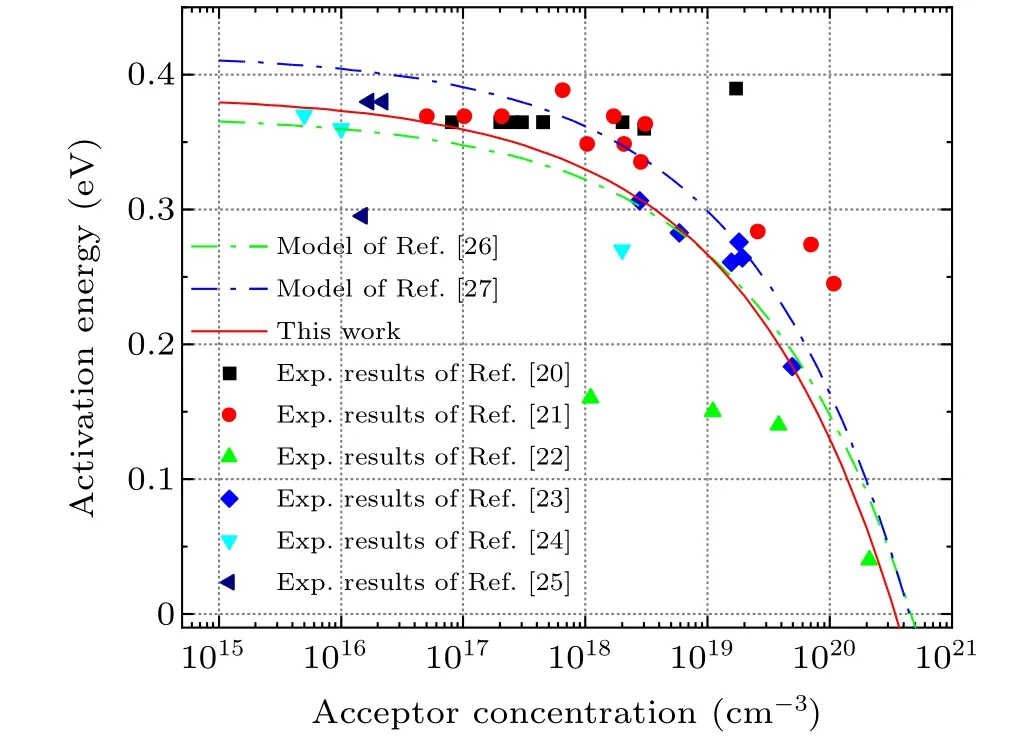
Fig.1.Fitting results of the activation energy dependence on the acceptor concentration to experimental data[20-25] for B-doped diamond.Model results from Marechal et al.[26] and Hathwar et al.[27] are also given for comparison.
2.2.Impact ionization model
As is known to all,the carrier concentration in the depletion region would increase sharply for impact ionization when the electric field strength exceeds a certain level, and the device’s current would increase exponentially.The above physical phenomenon is generally referred to as avalanche breakdown and can be described using the impact ionization model.In this work,the Van Overstraeten-de Man impact ionization model was applied to the calculation,[13]which can be expressed as
whereGis the generation rate of carriers,n(p)is the concentration of electrons (holes),vn,pis the drift velocity for electrons(holes),andαn,pis the ionization coefficient for electrons(holes)which could be obtained froman(ap),bn(bp)andγ.
2.3.Carrier mobility dependency model
Carrier mobility has a significant impact on device performance.Due to the coexistence of various scattering mechanisms, the carrier mobility would change with doping concentration and electric field strength at room temperature.We embed a corresponding model in the Silvaco Atlas using the built-in C language interpreter to introduce this effect.For a specific doping concentration and electric field strength, we can calculate the corresponding carrier mobility with the following formulas:[26]
whereµh0andµhare the hole mobility without electric field or with electric field,Nimpis the doping concentration,Efis the electric field,vsatis the saturation velocity for the hole,andα,µmax,µmin,Nµ,βsatare the fitting parameters.
2.4.Light absorption and photogeneration model
The photogeneration model is used to calculate the optical properties of the device.The optical generation rate is calculated based on
wherePis the ray intensity factor,η0is the internal quantum efficiency,hνis photon energy andαis the absorption coefficient.In order to simulate the response spectra of the APD, the absorption coefficients at different wavelengths need to be introduced.It can be considered as a wavelengthdependent function and the following formula is generally used for fitting:[28]
whereα1,α2,E1,E2,Pare the fitting parameters.In this simulation, Ga2O3is used as the absorber layer as it is a direct bandgap semiconductor and its theoretical absorption coefficient is much larger than that of diamond.In order to make this article closer to the ideal conditions in the performance prediction of the device, and provide more reference value for the follow-up device preparation research, the absorption coefficients of Ga2O3are chosen by consulting the data of Ma,[29]which are obtained by first-principles calculations.And the absorption coefficients of diamond sources are taken from the results of Collins.[30]The corresponding fitting values are given in Table 2.
2.5.Tunneling model
The tunneling mechanism is a potential factor affecting the dark current characteristics of an APD.In general, bandto-band tunneling(BBT)and trap-assisted tunneling(TAT)are the main physical models for APD simulation.The BBT tunneling generation rate is[31]
whereEis the magnitude of the electric field,Dis a statistical factor,γis a user-definable parameter andα,βare parameters related to the bandgapEg.Due to the lack of reliable parameters measured in the current experiments for device simulation,the parameters of Ga2O3and diamond used in the simulation are extrapolated from the Si parameter,and the corresponding values are given in Table 2.
The TAT model is also considered in the model, and its tunneling generation rate can be expressed as[32]
whereEgis the bandgap of the semiconductor,m∗is the effective mass,Eis the magnitude of the local electric field,Ntis the trap density,Etis the trap energy, andMis the matrix element associated with the trap potential.Bulk trap states and interface trap states are considered in the simulations.The concentrations (energy levels) of bulk trap states in Ga2O3and diamond are 4.7×1014cm-3(Ec-0.62 eV)and 8×1013cm-3(Ev+0.31 eV), respectively.They refer to the data of Zhang[33]and Nath.[34]Since no reliable experimental interface state data have been found, the interface trap density in Ga2O3/diamond heterojunction is assumed to be 1×1014cm-2, and the trap energy level isEv(Ga2O3)+2.45 eV(the band center of Ga2O3).
In addition to the above models, additional physical effects such as band narrowing,[35]Shockley-Read-Hall recombination[36]and Auger recombination[37]are also considered in our simulation.Apart from the parameters calculated from the models described above or taken from the literature,the rest of the parameters adopt the default value in the software.
3.Results and discussion
3.1.Characteristics of the diamond SBD and Ga2O3/diamond diode
To verify the rationality of the physical model and revise the numerical parameters,we simulated the diamond SBD and the Ga2O3/diamond pn heterojunction diode.Impact ionization is one of the most important factors affecting the APD simulation.Several pieces of research have been reported for obtaining the fitting parameters of diamond,and Table 1 summarizes the results proposed by different authors.To select the proper values, a standard SBD reported in the literature[38]is simulated using those parameters.As shown in Fig.2,the diamond impact ionization coefficients in different works show great differences due to the distinctive measurement methods and calculation methods.For the same SBD structure,the breakdown electric field strength obtained by most of the impact ionization parameters is still relatively approximative,ranging from 1.8 MV/cm to 2.7 MV/cm,and agreeing with the experimental results of 3.1 MV/cm.Considering the closeness to the experimental results,we finally adopted the parameters proposed in Ref.[39].
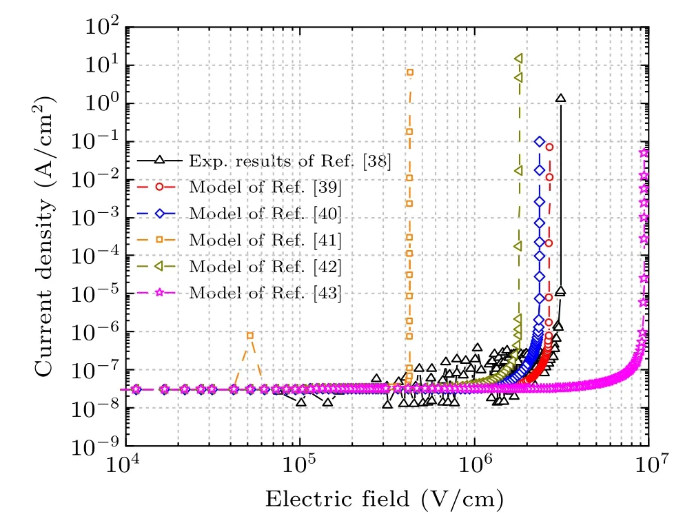
Fig.2.The diamond SBD reverse current-electric field characteristics obtained by experiment[38] vs.simulation with different ionization coefficients.[39-43]
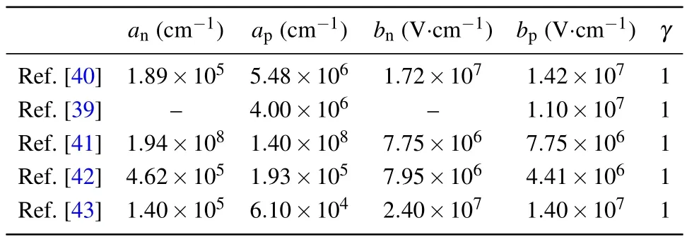
Table 1.Parameters of the impact ionization model proposed in the literature,an,ap,bn and bp are the parameters in formulas(5)and(6).
Next,aβ-Ga2O3/diamond heterojunction diode[7]is simulated.In this structure, the doping concentrations of ntype Ga2O3and p-type diamond are 4×1017cm-3and 1×1016cm-3, respectively.The simulated forwardI-Vcharacteristics are shown in Fig.3(a).The SRH lifetime,the electron affinity and the contact distribution resistance are reasonably adjusted in the simulation, and a result close to the experimental data is obtained.Both the simulation and experimental results exhibit similar turn-on voltage (~3.6 V), leakage current (~10-13A) and turn-on current (~0.1 mA).However, the current of the actual device in the logarithmic scale will increase when the load voltage exceeds 1.4 V,which does not appear in the simulation.It may be related to the leakage current caused by the generation-recombination process and the tunneling process due to the existence of complicated high trap states near the heterojunction interface in the actual devices.[44,45]The deviation perhaps stems from the simplified trap states we adopted in the model as the corresponding experimental parameter reports are scarce.
The simulated results of Fig.3(b) refer to the device of Kimet al.,[9]and the doping concentrations of n-type Ga2O3and p-type diamond are 1×1017cm-3and 1×1019cm-3,respectively.In general,the theoretical intrinsic carrier concentration for the wide-bandgap semiconductor should be lower than 10-20cm-3,but this would cause the inverseI-Vcharacteristic simulation to fail to converge.Therefore, in this simulation,we make an appropriate compromise in the minimum intrinsic carrier concentration for both diamond and Ga2O3.In addition,the wavelength of incident light is 250 nm and the corresponding extinction factor is calculated byκ=λα/(4π).Although some deviations are still existing at low voltages,which may be related to the deviation in some model parameters, the simulation results are generally in agreement with the experimental result,indicating that the physical model and material parameters used for the simulation are acceptable.
Figure 3(c)shows the spectral responsivity characteristics consistent with the device structure of Suzukiet al.[46]It can be seen that the responsivity of the Ga2O3photodetector in the simulation will drop rapidly around 250 nm,which corresponds to the band gap of Ga2O3.The simulation results are basically in agreement with the experiment,which proves the rationality of the diamond material model and the parameters we use.Some deviations still exist between the experimental results and the simulation results,and this can be attributed to the parameters of the absorption coefficient we adopted in the simulation source being from theoretical absorption spectra obtained by first-principles calculations, which could be different from the value in actual material due to the existence of defects.As a theoretical simulation,we hope to avoid the influence of uncertain factors on our calculation results as much as possible, so the absorption coefficient closer to the ideal Ga2O3is preferred in our simulation.Although deviation exists, it should be reasonable and would not affect the validity of the device simulation.
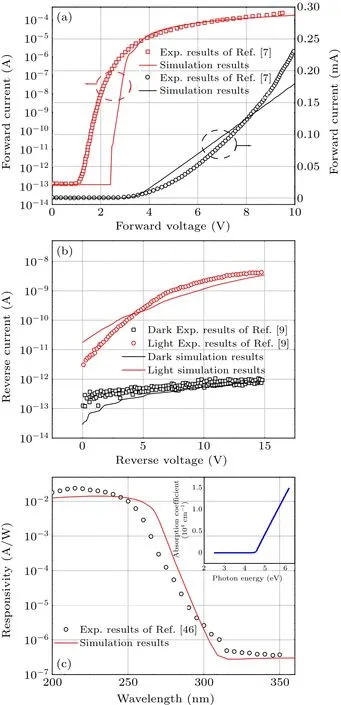
Fig.3.Simulation results of (a) the forward I-V characteristics for the Ga2O3/diamond diode fabricated by Sittimart et al.[7] Both linear and logarithmic coordinates are used in the Y-axis to show fit deviations at high and low currents, respectively.(b) The reverse I-V characteristics of the Ga2O3/diamond photodiode fabricated by Kim et al.[9] (c)The response spectra of the Ga2O3 photodiode made by Suzuki et al.
Table 2.Parameters adopted in TCAD simulation.
In brief, Table 2 summarizes the optimized material parameters obtained in the above repeating comparison.By simulating the diamond SBD and Ga2O3/diamond diode (photodiode), several physical parameters have been corrected and the reliability of the simulation and prediction for the Ga2O3/diamond heterostructure APD could be greatly enhanced.
3.2.Simulation and prediction of the Ga2O3/diamond APD
Figure 4 shows the designed structure of the Ga2O3/diamond heterostructure APD, which refers to the device dimensions of Refs.[11,53].For 2D simulation,the default length of the software in the third dimension is 1 µm.The device adopts the SAM structure, in which the doping concentrations of the contact layer, absorption layer,charge layer,multiplication layer and substrate layer are 1×1018cm-3,1×1015cm-3,4×1017cm-3,1×1015cm-3and 3×1019cm-3,respectively.
Figure 5 shows the electric field distribution and the band structure of the device.To eliminate the edge breakdown effect, we introduce the mesa structure.As shown in Fig.5(a), we can see that the maximum electric field in diamond is located inside the multiplication layer with the value of 3.82 MV/cm at 250 V, and the electric field concentration problem on the edge of the multiplication layer is alleviated,which avoids premature breakdown of the device.This structure could ensure that the APD can operate at higher voltages,resulting in a greater gain.

Fig.4.Schematic diagram of the Ga2O3/diamond heterostructure APD.Lu: length of the mesa top;Lb: length of the mesa bottom;Ls: length of the diamond substrate; Ho: thickness of the contact layer; Ha: thickness of the absorption layer;Hc: thickness of the charge layer;Hm: thickness of the multiplication layer;Hs: thickness of the diamond substrate.
The internal gain is derived from the hole-dominated avalanche ionization in the diamond multiplication layer.In this APD,the holes mainly originate from the Ga2O3absorption layer.When irradiated by suitable UV light, photogenerated electron-hole pairs will be generated in the Ga2O3absorption layer, and then will be separated due to the biased electric field, in which the holes will drift to the diamond and trigger impact ionization in the high electric field.It is necessary to control the electric field to ensure the safety of Ga2O3when the diamond is in breakdown.Thus, we introduced a 0.2 µm charge control layer between the Ga2O3absorption layer and the diamond multiplication layer.As shown in Fig.5(b), the charge layer is gradually depleted with increasing bias voltage, which finally reduces the electric field strength by 1 MV/cm.
Besides,the rapid reduction of electric field strength can be seen in the Ga2O3/diamond interface.This is due to the formation of the heterojunction.In the simulation, the electron affinities of Ga2O3and diamond are 0.5 eV and 4 eV,respectively, and the bandgaps of Ga2O3and diamond are 4.9 eV and 5.47 eV,respectively.As shown in Fig.5(c), a staggered heterostructure (type-II) favorable for the drift of holes from the gallium oxide absorber layer to the diamond multiplication layer will be formed at the interface between Ga2O3and diamond,and its conduction band offset(ΔEc)and valence band offset(ΔEv)are 3.59 eV and 2.96 eV,respectively.Due to the tiny width of the junction, a small load voltage could cause a huge reduction of electric field strength in this region,and this effect would become more noticeable as the voltage increases.
Figure 6 shows theI-Vcharacteristics and avalanche gain of the device.The punch-through voltage of the device is about 100 V, where the charge layer will be completely depleted and the holes generated under the illumination will drift into the diamond and form the current(as shown in Fig.5(b)).As the loading voltage increases to 273 V, the abrupt current rising occurs with a tiny increase of reverse bias, which means that the device has avalanche breakdown.The dark current density will reach~10 A·cm-2, which is consistent with the result obtained by the Ga2O3/diamond photodiode for Kimet al.[9]The avalanche gain can be calculated using the multiplied light/dark current difference and the unmultiplied mean light/dark current difference.[54]According to theI-Vcurve obtained by simulation, the gain of the device can be greater than 5×10⁴(where the corresponding voltage and dark current density are 273 V and 1.1×10⁻⁵A·cm-2,respectively),which means that the actual responsivity of the device could be orders of magnitude higher than that of conventional Ga2O3/diamond heterojunction detectors.
It is worth noting that the avalanche voltage of the device will decrease when the doping concentration of the diamond substrate increases,as shown in Fig.6.When the doping concentration of the diamond substrate rises to 1020cm-3, the breakdown voltage of the device is only 186 V.It is primarily ascribed to the fact that the high free hole concentration will reduce the width of the depletion of the diamond substrate and thence more voltage will be applied to the multiplication layer at the same bias voltage.The ionized impurity concentration is dramatically dependent on the doping concentration in p+diamond.For instance,in our model,the free hole concentration of diamond atNA=1019cm-3is 5×1016cm-3,while the free hole concentration will be rapidly increased to 2×1018cm-3atNA=1020cm-3.This physical effect means the drop of breakdown voltage becomes particularly significant.It is obvious that lower breakdown voltage is more beneficial for the practical application of the APD, and thus a higher doping concentration should be selected.However,the metal-insulator transition for the p-type diamond at high doping concentrations also needs to be considered.[55]As a matter of fact,when the doping concentration of diamond reaches~1020cm-3, the diamond substrate might work as a metallic layer in the device, and the heterojunction diode would lose its rectification function which has been demonstrated inβ-Ga2O3/diamond p+n heterojunction diodes.[7]Hence, we suggest that the B-doping concentration of 3×1019cm-3is reasonable in our model,and the corresponding free hole concentration is 2×1017cm-3.
Figure 7 shows the response spectrum characteristics of the APD at 273 V obtained in the simulation.Due to the internal gain,the corresponding responsivity can reach 78 A/W(200 nm) in 273 V (while dark current density is about 1×10⁻⁵A·cm-2and breakdown has not yet occurred).The cutoff wavelength of APD(defined as when the responsivity decreases to the peak point 1/e of the device) is 263 nm, indicating that the device can work well in the solar-blind band.

Fig.6.The current and multiplication gain characteristics of the Ga2O3/diamond SAM-APD(the red line is photocurrent,the black line is dark current,and the blue line is gain curve).The inset shows the breakdown voltage with different diamond substrate doping concentrations.
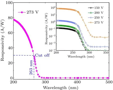
Fig.7.The photo response spectrum of the Ga2O3/diamond SAMAPD near the breakdown voltage, in which the optical power density is 1 mW·cm-2.The inset shows the response spectra under different biases with logarithmic scale in the Y-axis.
4.Conclusion
In this paper, we build a calibrated physical model for the simulation of a Ga2O3/diamond heterostructure.A Ga2O3/diamond SAM-APD with specific doping distribution was simulated based on the model.The device requires only n-Ga2O3and p-diamond,and the mesa structure is used to optimize the electric field distribution to avoid premature breakdown.TheI-Vcharacteristics, gain characteristics and spectral response characteristics are given.Benefiting from the gain brought by impacting ionization in the diamond multiplication layer,the responsivity can reach 78 A/W.The cutoff wavelength of the device is 263 nm, indicating its suitability for solar-blind detection.
Acknowledgments
Project supported by the National Key Research and Development Program of China(Grant No.2022YFB3608602),the Beijing Municipal Science and Technology Commission(Grant No.Z181100004418009), and the National Natural Science Foundation of China(Grant No.61927806).
杂志排行

Chinese Physics B的其它文章
- Single-qubit quantum classifier based on gradient-free optimization algorithm
- Mode dynamics of Bose-Einstein condensates in a single-well potential
- A quantum algorithm for Toeplitz matrix-vector multiplication
- Non-Gaussian approach: Withstanding loss and noise of multi-scattering underwater channel for continuous-variable quantum teleportation
- Trajectory equation of a lump before and after collision with other waves for generalized Hirota-Satsuma-Ito equation
- Detection of healthy and pathological heartbeat dynamics in ECG signals using multivariate recurrence networks with multiple scale factors