High-performance artificial neurons based on Ag/MXene/GST/Pt threshold switching memristors
2023-02-20XiaoJuanLian连晓娟JinKeFu付金科ZhiXuanGao高志瑄ShiPuGu顾世浦andLeiWang王磊
Xiao-Juan Lian(连晓娟), Jin-Ke Fu(付金科), Zhi-Xuan Gao(高志瑄),Shi-Pu Gu(顾世浦), and Lei Wang(王磊),†
1The College of Integrated Circuit Science and Engineering,Nanjing University of Posts and Telecommunications,Nanjing 210023,China
2The National and Local Joint Engineering Laboratory of RF Integration and Micro-Assembly Technology,Nanjing University of Posts and Telecommunications,Nanjing 210023,China
Keywords: memristors,artificial neurons,2D MXene,Ge2Sb2Te5
1. Introduction
In recent years, with the vigorous development of the artificial intelligence technology, the brain-inspired computing architecture based on an artificial neural network (ANN)that surpasses the traditional von Neumann architecture has attracted great interest of researchers due to its integration of memory and processor with high parallel computing capability.[1–4]Unlike ANNs, the spiking neural networks (SNNs) exhibit the most similarity to biological brain,and the operational power of the SNN is exclusively consumed when the neuron is triggered,allowing for much lower power consumption.[5–7]For hardware-based SNNs,integrate and fire neurons are usually considered as spike neurons,[8]which can be realized through resistive random-access memory(RRAM),[9]phase change RAM(PCRAM)[10]and threshold switching (TS) memristor.[11–13]Compared with nonvolatile memory-based neurons that require an additional circuit to complete the reset operation, the TS memristor shows automatic reset function,which greatly reduces the power consumption and circuit cost.[14–16]
Chalcogenide compounds represented by Ge2Sb2Te5(GST)have been widely used in the PCRAM because they can be rapidly and reversibly switched between the crystalline and amorphous states by current and laser pulses, and have good durability.[17–20]Electrochemical metallization (ECM) kinetics is generally difficult to change due to its fixed dielectric layer material. Therefore, the different GST-based ECM devices arising from its unique electrical and optical characteristics are recently designed for the reconfigurable and braininspired system applications.[21–27]However, the possibility of applying the GST-based TS memristor to artificial neurons is yet to be reported. In this article,we strategically prepare an Ag/MXene/GST/Pt memristor by inserting a 2D material MXene (Ti3C2) into the Ag/GST/Pt device to reduce the power consumption.[28,29]The Ag/MXene/GST/Pt memristor with an extremely steep slope(<0.1 mV/dec)and a large off/on ratio(>103)has lower switching voltage and current compared to the Ag/GST/Pt memristor. In addition,the integrate and fire neurons that are indispensable for the SNNs have been experimentally demonstrated in a single Ag/MXene/GST/Pt device without additional circuit to complete the function of integration. Finally, the first-principles calculation accompanied by electrochemical metallization effect has been used to explain electrical characteristics. This work provides a useful guideline for achieving an artificial hardware-based SNN.
2. Experimental details
The studied Ag/GST/Pt and Ag/MXene/GST/Pt crossbar structures are fabricated on the Si wafer,as shown in Figs.1(a)and 1(b), respectively. Firstly, the Pt bottom electrode with a thickness of 100 nm is deposited by DC magnetron sputtering at ambient temperature. Next,the GST layer with a thickness of 50 nm is deposited by DC magnetron sputtering with Ar gas at a flow rate of 10 sccm and a pressure of 1 mtorr. Then,the MXene (Ti3C2) layer on the GST, prepared by etching Ti3AlC2with hydrogen fluoride (HF), is deposited by spincoating at 1500 rpm for 120 s. The main component of the 2D MXene is Ti3C2according to the x-ray diffraction(XRD)results in Fig.1(c). Figure 1(d)is a scanning electron microscope (SEM) image showing a MXene thin film spin-coated on a silicon wafer under the same spin-coating conditions.The thickness of the spin-coated MXene thin film is about 50 nm. Finally, the metallic Ag with a thickness of 100 nm is deposited by DC magnetron sputtering as the top electrode.Subsequently the studied Ag/GST/Pt and Ag/MXene/GST/Pt devices are heated to 300°C and annealed for one hour in a vacuum environment.The area of the intersection between the top electrode and the bottom electrode is 100×100 μm2. The XRD patterns of the GST material before and after annealing reveal the presence of amorphous and crystalline phases before and after the annealing,as depicted in Figs.1(e)and 1(f),respectively. The threshold switching phenomenon is only observed in both Ag/GST/Pt and Ag/MXene/GST/Pt devices after the annealing treatment.Therefore,it can be known that the metal conductive bridges are more likely to be generated inside the MXene and the crystalline GST layers.All the electrical properties of the Ag/GST/Pt and Ag/MXene/GST/Pt memristors are measured by Keithley 4200A-SCS semiconductor parameter analyzer with the Pt bottom electrode grounded.
3. Results and discussion
Cycling measurements are performed on the Ag/GST/Pt and Ag/MXene/GST/Pt devices under the current compliance limits of 10 mA and 5 μA,respectively,as shown in Figs.2(a)and 2(b). Here a DC sweep rate of 0.15 V/s is used for cycling measurement. Although the Ag/GST/Pt device exhibits good cycle endurance and stable bi-directional TS characteristics, relatively large set voltage (1.6 V) and current(1.4 mA) are still found. Therefore, we further fabricate the Ag/MXene/GST/Pt device by inserting a 2D material MXene(Ti3C2)into the Ag/GST/Pt device. Such Ag/MXene/GST/Pt device has a lower set voltage(0.38 V)and current(200 nA),thus considerably reducing the power consumption(Fig.2(b)).It is worth noting that the distribution of set voltages in positive polarity is significantly more concentrated than that in negative polarity. This is because the Ag ions previously trapped in the GST layer after the positive voltage sweep will move back towards the Ag top electrode and eventually reform a conductive bridge under the negative voltage sweep. However, owing to the absence of a stable Ag ions source in this situation,resulting conductive bridges are formed more randomly inside the GST layer,causing such discrepancy of the set voltages in the negative polarity. Furthermore,it can be observed that most of set voltages are concentrated between 0.2 V and 0.4 V for the Ag/MXene/GST/Pt device in the positive polarity, leading to the set power consumption range from 10 nW to 100 nW.
In addition, 300 cycles DC voltage sweeps are used to evaluate the endurance performance of the Ag/MXene/GST/Pt device, as shown in Fig. 2(c). The values of resistance and current are extracted at the point of threshold switching,confirming the excellent reliability of the Ag/MXene/GST/Pt device. Pulse amplitude modulation approach has been widely adopted to dynamically tailor the resistances of memristors;thus,we further investigate the endurance performance of the Ag/MXene/GST/Pt device using current pulse operation. Different pulse amplitudes of 5 μA, 10 μA and 50 μA with the same pulse width of 20 ms and interval of 20 ms are applied into the Ag/MXene/GST/Pt device.Resulting resistance states are shown in Figs. 2(d), 2(e), and 2(f), respectively. It is observed that using larger pulse amplitude gives rise to more stable resistance states, and the off/on ratio is larger than 103.This is because the resulting electric field arising from the small pulse amplitude may not be sufficiently strong to drive the Ag ions to form a conductive bridge within the short period of 20 ms. Nevertheless, this situation can be attractively improved when the pulse amplitude reaches 50 μA. Therefore,choosing the appropriate pulse amplitude and pulse width can remarkably benefit the reliability and operational performances of the designed device without the sacrifice of the energy consumption.
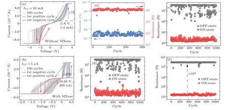
Fig.2.Typical TS I–V characteristics of(a)the Ag/GST/Pt memristor and(b)the Ag/MXene/GST/Pt memristor.(c)The endurance performance of the Ag/MXene/GST/Pt device using 300 cycles DC voltage sweeps. On and off resistance states by using current pulse operation with amplitudes of(d)5 μA,(e)10 μA and(f)50 μA for write and of 10 nA amplitude for read. Pulse width and interval were both set to be 20 ms.
Furthermore, the multi-level conductance behaviors are secured by employing four continuous positive voltage sweeps with stop voltage of 0.5 V and negative voltage sweeps with stop voltage of-1.6 V, as shown in Figs. 3(a) and 3(b). A gradual increase on the conductance of the Ag/MXene/GST/Pt device is found,indicating that the device has the capability of continuous conductance modulation. Figure 3(c) shows DC stress test of the Ag/MXene/GST/Pt device at room temperature. The high resistance state can be maintained about 104s under the read voltage of 0.05 V. Besides, we perform slow sweep (9 mV/s) with high sampling rate and identify a set slope of<0.1 mV/dec(Fig.3(c)). These results undoubtedly demonstrate the practicality of using the Ag/MXene/GST/Pt device for a low-power selector device in the application of neuromorphic circuits.

Fig.3. (a)The measured I–V curves for positive voltage sweeps with stop voltage of 0.5 V.(b)The measured I–V curves for negative voltage sweeps with stop voltage of-1.6 V.(c)DC stress test of the Ag/MXene/GST/Pt device. Blue dots and red dots refer to the current at the off state and corresponding resistance value,respectively. (d)Set slope measurement under slow sweeping with high sampling rate.
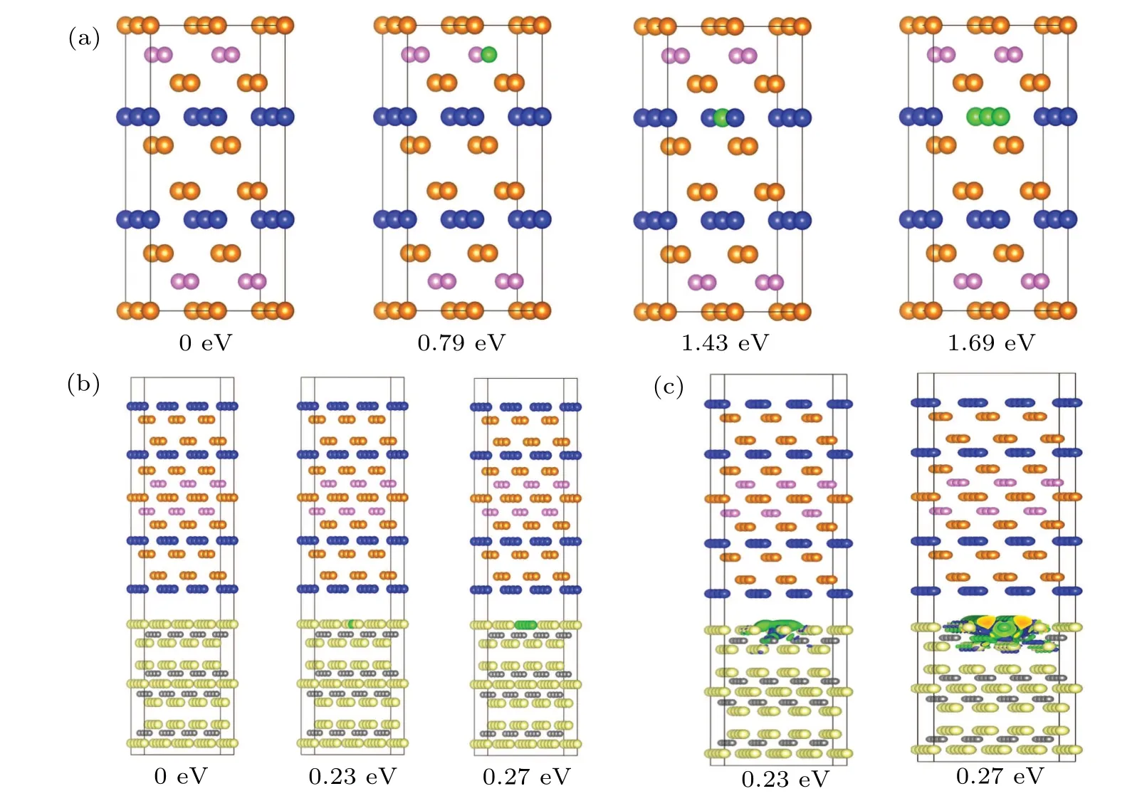
Fig.4. (a)Structural models and required formation energies of the pristine GST compound and the Ag-doped GST compounds. Te, Sb, Ge, and Ag atoms are represented by golden,blue,pink,and green balls,respectively. (b)Structural models and required formation energies of the pristine Ti3C2/GST heterojunction and the Ag-doped Ti3C2/GST heterojunctions. Te, Sb, Ge, Ag, Ti, and C atoms are represented by golden, blue, pink,green,yellow,and gray balls,respectively. (c)Differential charge analyses. Te,Sb,Ge,Ag,Ti,and C atoms are represented by golden,blue,pink,green,yellow,and gray balls,respectively. Left and right sections of(c)correspond to the middle and right sections of(b),respectively.
To better understand the physical mechanism that governs the TS characteristics of the Ag/MXene/GST/Pt device, the first-principles calculations were carried out by using density functional theory(DFT)with generalized gradient approximation(GGA)of Perdew–Burke–Ernzerhof(PBE)implemented in the Viennaab-initiosimulation package(VASP).[30,31]The valence electronic states were expanded on the basis of plane waves with the core-valence interaction represented by using the projector augmented plane wave (PAW) approach[32]and a cutoff energy of 550 eV. AΓ-centeredk-mesh of 2× 2×2 was used for bulk calculations. Convergence was achieved when the forces acting on ions became smaller than 0.05 eV/˚A.An electric field of 107V/m was included to consider the effects of the applied electric field in practice.
As can be seen from Fig.4(a),the formation energy continuously increases along with the extension of the Ag ion cluster, and a complete grow requires a formation energy of 1.69 eV.This evidently implies the difficulty in the direct substitution of the Ag ions on both Ge and Sb sites at low temperatures. However,the formation energy of the Ag ion cluster is considerably reduced for the Ti3C2/GST heterojunctions,leading to a formation energy of 0.27 eV for a complete growth(Fig. 4(b)). Such fact obviously reveals that more energy is required for the substitution of the Ag ions on both Ge and Sb sites. Therefore, it can be speculated that the conductive filaments (CFs) generally grow in the MXene and GST layers with the applied voltage increasing, but the CFs are more likely to rupture in the GST layer with the applied voltage decreasing.
To further reveal the formation mechanisms of the Ag conductive bridges at the Ti3C2/GST heterojunctions,two differential charge analyses are performed,corresponding to the formation energies of 0.23 eV and 0.27 eV in Fig. 4(b), respectively. It is clear from Fig. 4(c) that there exists strong charge transfer between Ag ions and their coordinated carbon atoms. It is therefore evident that the Ti3C2can readily attract Ag ions due to their strong electrostatic interactions, which encouragingly benefits the formation of Ag conductive bridge across the designed device. In other words, MXene (Ti3C2)has a strong capability to absorb Ag ions, which can make it easier for Ag ions to enter the GST layer along the position of the MXene nanoparticles,thereby forming more stable and single Ag conductive filaments, while reducing the switching current and voltage.
The conduction mechanism of the TS memristor closely resembles the neural membrane dynamics, whereby they can promisingly simulate two vital functions of neuron, i.e., integrate and fire,as shown in Fig.5(a). By intensifying the external stimulation,the action potential of the neuron undergoes a huge change after a certain period,and the nerve signal can be transmitted. Triggered by this exciting imitation, the characteristics of the integrate and fire neurons that are essential for SNNs have been experimentally demonstrated, as illustrated in Figs. 5(b) and 5(c). A succession of positive pulses with different amplitudes(i.e.,a 2 μA and 3 μA triangle wave with a pulse width of 20 ms and pulse interval of 20 ms)are applied to the Ag/MXene/GST/Pt device. It is observed that the conductance gradually increases with the number of triangle wave pulses in the case of small external stimulus,and this process corresponds to the realization of the integrate function. Then the conductance increases sharply when the external stimulus increases,which realizes the function of fire.Moreover,due to the volatile nature of our TS devices, the Ag/MXene/GST/Pt devices show automatic reset function and automatically return to the initial state after the external stimulus disappears.
Table 1 shows the comparison of some TS memristors with the same ECM mechanism using Ag electrodes. Compared to other TS memristors, our Ag/MXene/GST/Pt devices show excellent performances, including smaller threshold switching parameters and extremely steep slope. At present, the application of TS memristor based on the GST material in selector has been reported.[33]However, the possibility of applying the GST-based TS memristor to artificial neurons is yet to be reported. Our work explores and complements the application prospects of the GST-based memristors in the field of integrate and fire neurons.
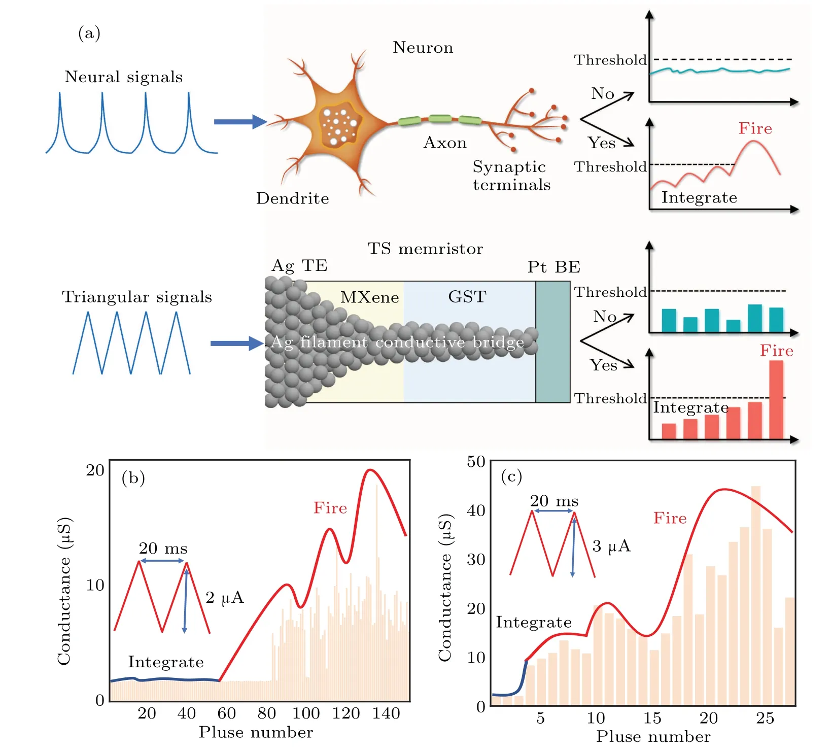
Fig.5.(a)Schematic diagram of the integrate-and-fire in a biological neuron,and the integrate-and-fire characteristics of the Ag/MXene/GST/Pt device. The integrate-and-fire artificial neuron is realized in the Ag/MXene/GST/Pt device using a succession of triangular wave pulses with different amplitudes of(b)2 μA and(c)3 μA,and the same pulse width of 20 ms and pulse interval of 20 ms.

Table 1. Comparisons of different TS devices with ECM mechanism.
4. Conclusion and perspectives
An artificial integrate and fire neuron has been demonstrated by using the Ag/MXene/GST/Pt memristor with excellent electrical characteristics, such as a low set voltage(0.38 V) and current (200 nA), an extremely steep slope (<0.1 mV/dec), and a relatively large off/on ratio(>103). Furthermore,its memristive mechanism is interpreted through the first-principles calculation with the electrochemical metallization effect.
Acknowledgements
Project supported by the National Natural Science Foundation of China (Grant Nos. 61804079 and 61964012), the open research fund of the National and Local Joint Engineering Laboratory of RF Integration and Micro-Assembly Technology(Grant No.KFJJ20200102),the Natural Science Foundation of Jiangsu Province of China(Grant Nos.BK20211273 and BZ2021031), the Nanjing University of Posts and Telecommunications (Grant No. NY220112), and the Foundation of Jiangxi Science and Technology Department(Grant No.20202ACBL21200).
猜你喜欢
杂志排行

Chinese Physics B的其它文章
- The coupled deep neural networks for coupling of the Stokes and Darcy–Forchheimer problems
- Anomalous diffusion in branched elliptical structure
- Inhibitory effect induced by fractional Gaussian noise in neuronal system
- Enhancement of electron–positron pairs in combined potential wells with linear chirp frequency
- Enhancement of charging performance of quantum battery via quantum coherence of bath
- Improving the teleportation of quantum Fisher information under non-Markovian environment