Half-metallicity induced by out-of-plane electric field on phosphorene nanoribbons
2022-08-01XiaoFangOuyang欧阳小芳andLuWang王路
Xiao-Fang Ouyang(欧阳小芳) and Lu Wang(王路)
School of Physics and Electrical Information,Shangqiu Normal University,Henan 476000,China
Keywords: half-metal,antiferromagnetic,two-dimensional materials,spin polarization
1. Introduction
Spintronics, which utilizes spin as the carrier for information transportation and processing, is one of the most promising methodologies in achieving high-speed and lowenergy-consuming electronic devices.[1–4]A key challenge in this field is generating fully spin-polarized current around the Fermi level. Half metal, where only one spin channel is conductive while the other is insulating, can resolve this problem.[5]Recently,graphene has attracted extensive research attention because of extraordinary thermal, mechanical, and electrical properties.[6,7]However, the dirac point is difficult to switch on at the room temperature,which impedes applications in spintronics. Therefore, in order to overcome this problem,much effort has been made to find semiconductor with large band gap. Transitional metal sulfide(TMS)with relatively high and adjustable band gap achieved by adjusting the number of layers and components of sulfide, may resolve this problem.[8–11]Moreover,the optical band gap of TMS has been proved to be dependent on the temperature.[12,13]Nevertheless, the carrier mobility of these materials is much lower than 200 cm2/V·s,[14]which hinder their application seriously.
Compared with the gapless graphene and silicene, black phosphorene has attracted great attention due to the thickdependent band-gap of 0.3 eV–2 eV.[15,16]On the other hand,in comparison with TMS, the black phosphorene has advantages of ultrahigh carrier mobility[17,18]and anisotropic thermal, optical, and electronic transport properties,[19–21]being excellent for application in spintronics.Furthermore,the fieldeffect-transistor(FET)based on few layer black phosphorus is found to have strikingly high on/off ratio of 105and a carrier mobility of 103cm2/V·s at the room temperature,[22]being beneficial for application in nano devices. Thus,phosphorene is becoming a potential material in the field of electronics,optoelectronics and spintronics due to the existence of above novel properties.[23,24]
It is well-known that the pursuit on controlled magnetism of phosphorene in practise has been persisting goal in the field of spintronics. Many theoretical researches about the magnetism of phosphorene have been proposed to date. The doping black phosphorene with substitutional impurities such as Ti,Cr,Ni,Mn and Fe is a ferromagnetic semiconductor,being the same as dilute magnetic semiconductor (DMS). The spin polarization of 100%is achieved in the phosphorene nanoribbons doped with Ti, Cr, Mn, Co and Fe atoms.[25]Besides,the O2-(Co-phosphorene)[26]and V doped phosphorene[27]show half-metallic characteristics. However, the macroferromagnetism originated from the magnetic atoms is unfavorable for the application in nano devices.[28,29]Spin polarization introduced by non-magnetic impurities in phosphorene may resolve this problem,[30,31]in fact,it is difficult to control the doping site accurately.
To better understand the effect of magnetism on electronic structure, the intrinsic magnetic properties of ZBPNRs are investigated in detail.[32–34]The antiferromagnetic ground state with ferromagnetic along same edge and antiferromagnetic between two opposite edges is found at the edge of ZBPNRs.[33]In addition, in-plane transverse electrical field has strong influence on the electronic structure of the ZBPNRs,resulting in the formation of topological insulate state.[35,36]Half-metallicity could be achieved in zigzag phosphorene nanoribbons with different groups decoration such as OH-NO2and NH2-NO2,[37]which avoid the drawback of macro-ferromagnetism deriving from the transitional metal atoms. Nevertheless,it is difficult to obtain the selective modification in experiment. Therefore,the study of the half-metal based on black-phosphorene without transitional metals,substitutional doping and magnetic field is utmost imperative.
In this work,we present a systematic investigation on the electronic and magnetic properties of ZBPNRs by applying density functional theory. The widths of ZBPNRs are classified by the number of P atom across the ribbon width, as shown in Fig. 1(a). In order to obtain the magnetic ground state, non-magnetic and four different magnetic states displayed in Figs. 1(a)–1(d) are considered in the calculations.The ground state of ZBPNRs is dependent on the widths, as shown in Fig. 1(e). As for the narrow widths smaller than 8ZBPNRs,its ground state prefers the AFM1 order. With increasing of widths of ZBPNRs, the degeneracy between the AFM2 and AFM3 is formed, becoming the ground state, as shown in Fig. 1(e). More interesting, the addition of out-ofplane electric field can modulate the magnetic property, resulting in the split of antiferromagnetic degeneracy of AFM1 and realization of half-metal. Our results suggest a new way to obtain half-metal in the absence of transitional metal atoms,magnetic field and edge passivation, which is helpful in the construction of two-dimensional half-metal in spintronics.
2. Methods
Our investigation of ZBPNRs is all performed through Viennaab initiosimulation package[38,39]based on the projector augmented wave method.[40]The generalized gradient approximation(GGA)for the exchange–correlation functional are employed with plane wave energy cutoff of 500 eV.[41]The energy convergence criteria for electronic iterations is set to be 10-6eV. In the self-consistent potential calculation under electric field,8ZBPNRs of zigzag sheet with a set of 30×1×1 Monkhorst–Packk-points grid is used for Brillouin-zone integration,and when the density of states(DOS)is calculated,a 60×1×1k-point sampling is used.A vacuum space of at least 15 ˚A was included in the unit cell to eliminate the coupling between neighboring cells. The electronic and magnetic properties of ZBPNRs with ranging from 4ZBPNRs to 20ZBPNRs are investigated in detail. The widths of ZBPNRs are referred according to the number of P atoms in the direction perpendicular to the zigzag edge. All atomic positions and the sizes of phosphorene are optimized until the atomic force becomes smaller than 0.01 eV/ ˚A.

Fig.1. (a)FM,(b)AFM1,(c)AFM2,(d)AFM3 are initial magnetic structures adopt for searching magnetic ground state. (e)The energy difference of five magnetic states as a function widths of ZBPNRs.
3. Results and discussion
The relaxed lattice constants of monolayer black phosphorene are 3.2989 ˚A and 4.6291 ˚A,which are in good agreement with other theoretical calculations.[33,34,42]The ZBPNRs is obtained by cutting the monolayer black phosphorene along zigzag direction. For searching the ground state,five different magnetic states including NM,FM,AFM1,AFM2 and AFM3 are calculated by spin-polarized GGA calculation. As shown in Fig.1,AFM1 is ferromagnetic within each edge but antiferromagnetic between two opposite edges. AFM2 is intra-edge antiferromagnetic with inter-edge ferromagnetic,while AFM3 is the state with both intra-edge and inter-edge antiferromagnetic arrangements. The total energies of nonmagnetic(NM),ferromagnetic(FM),and various antiferromagnetic(AFM)orders were calculated, respectively. It was found that the stable magnetic states could be achieved by allowing the system to be spin polarized. Both the AFM and FM configurations are in energy lower than NM state regardless of widths of the nanoribbons,indicating that spin polarization is a possible stabilization mechanism.
More interesting, the ground state is dependent on the nanoribbon widths. Figure 1(e) shows the energy differenceEtotal-EAFM1per unit cell as a function of widths of nanoribbons. We can see that the AFM1 is ground state for the narrow nanoribbons with ranging from 4ZBPNRs to 8ZBPNRs.With increase of widths, AFM2 and AFM3 form a degenerate state with lowest total energy shown by red and blue line in Fig. 1(e), becoming the magnetic ground state, which manifest the weak interaction between two edges. The NM and FM will never be the ground state due to the dangling bond of edge atoms. The energy difference between the FM and AFM1 antiferromagnetic order marked by black line in Fig. 1(e) decreases with increase of widths and almost vanishes for 14ZBPNRs, because nanoribbon widths exceed the decay length of the spin polarization. Similar result was also found in pristine ZGNRs.[43,44]
To give a further insight of the magnetism of pristine ZBPNRs, the electronic structures of NM, FM and AFM1 of 16ZBPNRs are calculated in detail. Figure 2(c) shows that two bands from the edge P atoms across the Fermi level result in metallic character of NM state. For analyzing the contribution of edge atoms,the orbital band structure is calculated.As shown in Fig. 2(d), we can see that the states around the Fermi level are mainly contributed by the electrons of pzorbital due to the dangling bonds. In the FM state, the spin up and spin down channels are pushed away from the Fermi level to higher and lower energies, as shown in Fig.2(b). An indirect band gap is realized in the AFM1 state owing to the spilt ofαandβbands, in which the valence band top atΓpoint and the conduction band bottom at theXpoint,as displayed in Fig.2(a).
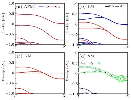
Fig.2. The band structure of 16ZBPNRs with AFM1 state(a),FM state(b),NM state(c),and(d)the orbital band structure of NM state.
The spin density (SD) and partial density of states(PDOS)of 16ZBPNRs with AFM2 state are calculated. In the AFM2 state,theαandβbands are split just above and below the Fermi level, forming a semiconductor shown in Fig.3(c).The SD shown in Fig. 3(a) reveals the spatial distribution of both dangling bond states and the tails of the spin-polarized p-orbital states. It is obvious that the magnetic moment at the edge arises from both dangling bonds as well as edge localized p-orbital states. As shown in Fig. 3(b), the magnetism is mainly contributed by the edge atoms with 0.25μBand-0.25μB, respectively, resulting in a total absolute magnetic moment of 1μB, while the contribution of its adjacent atoms to the local magnetic moments are small with 0.009μBand 0.005μBin a unit cell,respectively.
For analyzing the effect of electric field on magnetism of ZBPNRs, the electronic structure and magnetic properties of 8ZBPNRs with AFM1 state under electric field are calculated in detail. Table 1 shows that the total magnetic moment increased under the electric field due to the split of degeneracy of magnetic moment between opposite edge atoms, resulting the ferromagnetism of ZBPNRs, while the ferromagnetism disappears until the electric field increases to 4 V/nm. Figures 4(a)–4(c)indicate that the antiferromagnetic degeneracy is split by the out-of-plane electric field perpendicular to the ZBPNRs. As spin splitting energy increases with strength of electric field,the half-metallic ZBPNRs with about 0.2 eV half-metallic gap is achieved under the electric field with 3 V/nm. To further understand the atomic contribution to spin polarization, the PDOS under out-of-plane electric field with 3 V/nm are also calculated. Figure 4(d) shows that the edge atoms contribute significantly to the spin polarization, leading to the realization of half-metal with net spin down magnetic moment.
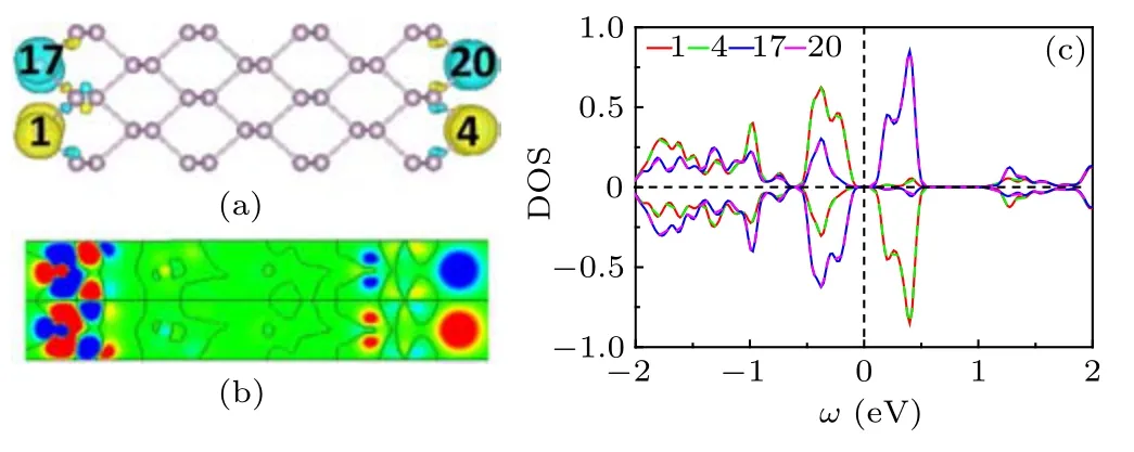
Fig.3. The SD(a),the projection of SD on the upper layer(b)(red and blue represent spin up and spin down,respectively),(c)the PDOS of 16ZBPNRs with AFM2 state. The edge atoms are represented as No. 1, 4, 17 and 20,respectively.

Fig. 4. The band structure of AFM1 state under electric field with 2 V/nm (a), 2.5 V/nm (b) and 3 V/nm (c), respectively. (d) The PDOS of edge atoms under the electric field with 3 V/nm, (e) the SD difference of 8ZBPNRs with AFM1 state under electric field ((ρup-ρdown)3 V/nm-(ρup-ρdown)0 V/nm), (f) the model under electric field. The red and green arrows indicate the spin direction.
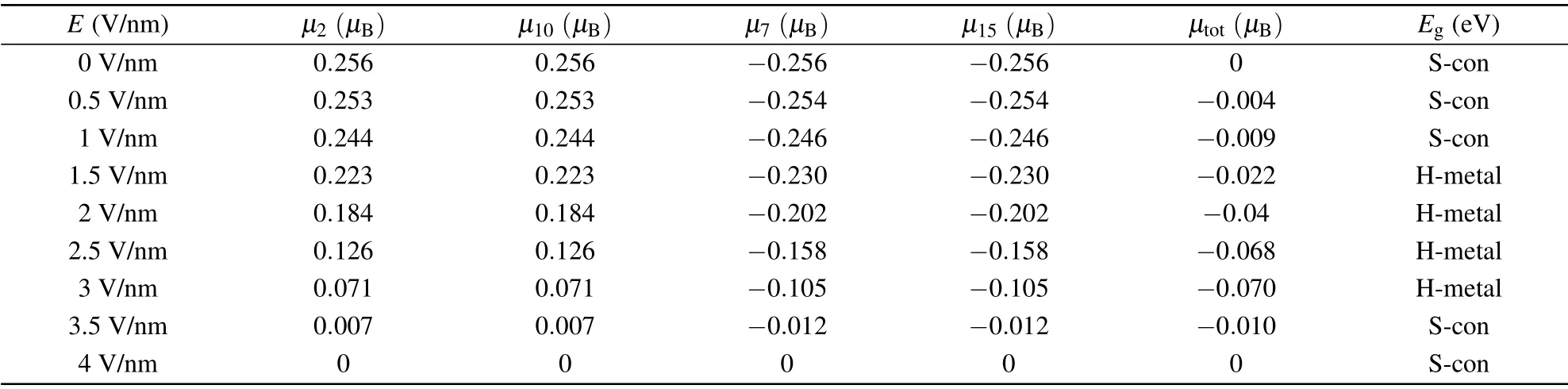
Table 1. Calculated magnetic moment under different electric field: magnetic moment of edge atoms((μ2(μB)),(μ10(μB)),(μ7(μB))and(μ15(μB))),the total magnetic moment of the system(μtot(μB)). Semiconductor and half-metallic structures are denoted as S-con and H-metal,respectively.
The SD difference of 8ZBPNRs with AFM1 state between 3 V/nm and 0 V/nm is calculated.As shown in Fig.4(e),it is obvious that the spin-up charge density around No.2 and No. 10 decrease, while the spin-up charge density at No. 7 and No.15 atoms increase under the electric field. In order to probe the intrinsic mechanism,the magnetic moment are summarized in Table 1. We can see that when the electric field increase to 3 V/nm,the magnetic moments of No.2 and No.10 decrease from 0.25μBto 0.071μB, while this value of No. 7 and No. 15 reduce from-0.25μBto-0.105μB, resulting in net magnetic moment of about-0.07μBand the realization of half-metal. From Fig. 4(f), we come to a conclusion that the staggered potential applied by out-of-plane electric field are different for the opposite edges owing to the different horizontal plane,inducing the split of spin degeneracy as well as achieving of half-metal.
The ZBPNRs with intra-edge ferromagnetic state and inter-edge antiferromagnetic order becomes half-metal under the action of out-of-plane electric field. This method is more advantageous in contrast to other complicated requirements such as select modification,transition metal doping,magnetic field, semihydrogenations and nitrogenations. In addition, in comparison with gapless graphene as well as TMS with small carrier mobility,the spintronic devices based on phosphorene have the advantage of high carrier mobility and high on/off ratio.The realization of half-metal based on phosphorene,which is independent on macroscopic ferromagnetism and selective doping,may expand the research scope of spintronic devices.
4. Conclusions
In conclusion, we have investigated the intrinsic electronic structure and magnetic properties of the ZBPNRs. We found that the antiferromagnetic state with intra-edge ferromagnetic and inter-edge antiferromagnetic is the ground state for the narrow widths and the half-metallic phosphorene is achieved by applying the out-of-plane electric field other than magnetic metal doping, defects, magnetic field and selective hydrogenation. Our findings may propose a new way to construct the nanoscale spintronic devices based on black phosphorene.
Acknowledgment
This work is supported by Key Scientific Research Projects of Colleges and Universities in Henan Province,China(Grant No.21A140022).
猜你喜欢
杂志排行

Chinese Physics B的其它文章
- Real non-Hermitian energy spectra without any symmetry
- Propagation and modulational instability of Rossby waves in stratified fluids
- Effect of observation time on source identification of diffusion in complex networks
- Topological phase transition in cavity optomechanical system with periodical modulation
- Practical security analysis of continuous-variable quantum key distribution with an unbalanced heterodyne detector
- Photon blockade in a cavity–atom optomechanical system