Introducing voids around the interlayer of AlN by high temperature annealing
2022-08-01JianweiBen贲建伟JiangliuLuo罗江流ZhichenLin林之晨XiaojuanSun孙晓娟XinkeLiu刘新科andXiaohuaLi黎晓华
Jianwei Ben(贲建伟), Jiangliu Luo(罗江流), Zhichen Lin(林之晨), Xiaojuan Sun(孙晓娟),Xinke Liu(刘新科),‡, and Xiaohua Li(黎晓华)
1College of Materials Science and Engineering,Shenzhen University-Hanshan Normal University Postdoctoral Workstation,Shenzhen University,Shenzhen 518060,China
2College of Physics and Optoelectronic Engineering,Shenzhen University,Shenzhen 518060,China
3State Key Laboratory of Luminescence and Applications,Changchun Institute of Optics,Fine Mechanics and Physics,Chinese Academy of Sciences,Changchun 130033,China
Keywords: AlN template,AlN interlayer,voids,high-temperature annealing
1. Introduction
The introduction of voids is an effective method to improve the light-emitting efficiency (LEE) of III-nitride-based light-emitting devices(LEDs), release the stress and improve the crystal quality of III-nitride-based materials.[1–6]Many researches have reported that the LEE of III-nitride-based LEDs was increased by introducing the air voids into LED structures.For example, the LEE of an InGaN-based LED with an airvoid-embedded SiO2mask was enhanced by 96.8%compared to that of a conventional InGaN-based LED.[7]Aliaset al.fabricated an AlGaN-based ultraviolet LED with nitride/air distributed Bragg reflector structure and found that the light output power (LOP) was improved by a factor of about 1.67.[8]Leeet al.fabricated an AlGaN-based LED on periodic airvoid-incorporated nanoscale-patterned sapphire substrate and the LOP was enhanced by 67%.[9]Based on the published reports,it was found that the introduction of voids is beneficial,i.e.,it increases the LEE of nitride-LEDs.
Researchers have adopted many methods to introduce voids into III-nitride materials, and most of the methods also effectively improve the quality of the III-nitride materials.The reported methods mainly include etching the substrate, using mask layers,decomposing the III-nitride materials and annealing the physical vapor deposited AlN(PVD-AlN).For example, Xieet al.and Yanet al.introduced voids during the epitaxial lateral overgrowth(ELO)of AlN and GaN on patterned sapphire,respectively.[10,11]The patterned sapphire substrates were fabricated by etching. Moreover, Caoet al.introduced voids into the a-plane GaN layer by etching the a-plane GaN templates.[12]Furthermore, the adoption of a mask layer is a common method to introduce voids, such as the growth of GaN or AlN on a patterned SiO2mask or van der Waals substrates, respectively.[13,14]The voids were formed during the growth process due to the difficulty of nucleation on the masks. Both methods mentioned above were used to achieve ELO of III-nitride materials. However, they require complex pretreatment of the substrates,and the epitaxial layers should be thick in order to form a flat surface. The decomposition of GaN is an effective method to introduce voids into AlGaNbased materials. Liuet al.introduced voids into the GaN layer by decomposing the GaN in H2,and Mitsunariet al.fabricated air voids by decomposing the GaN in GaN/AlN core-shell structure in order to grow GaN using the ELO method.[15,16]Recently,high-temperature annealing(HTA)has proved to be an effective and simple method to obtain high-quality AlN template, and the voids were introduced into PVD-AlN layer during HTA.[17–20]The formation mechanism of the voids has been explained as the coalescence of the crystal grains or the annihilation of the dislocations during recrystallization.However, it is difficult to obtain high-quality AlGaN-based materials using the PVD method directly. Considering that the AlGaN-based epitaxial structures are commonly grown by metal-organic chemical vapor deposition (MOCVD),out situdeposition process will be required if adopting the PVD method to introduce voids into the AlN layer, which will increase the complexity. Consequently, to introduce voids at a certain height into the AlN layer by adopting the PVD method is also too complex.
In this work, to introduce the voids into the AlN layer at a controllable height, the AlN template with moderatetemperature AlN interlayer was designed and then annealed at 1700°C for one hour to induce the formation of voids,which was inspired by the formation mechanism of the voids in PVDAlN layer during the HTA process. The voids were introduced around the interlayer and the crystal quality of the AlN template improved. This work provides a potential simple method to introduce voids into AlN at a controllable height.
2. Experimental procedure
Thec-plane sapphire substrates were used to grow AlN layers by MOCVD(AIX 200/4 RF-S).NH3was used as the N precursor and TMAl was used as the Al precursor. First, the nucleation layer was grown at about 950°C with a V/III ratio of 11000. Then, the nucleation layer wasin situannealed at about 1330°C and the high-temperature AlN(HT-AlN)layer was grown at 1280°C with a V/III ratio of 1100. The AlN interlayer was grown at 1050°C with a V/III ratio of 3700.Finally, to introduce voids into AlN layer, the AlN template wasout situannealed at 1700°C for one hour in pure N2atmosphere.
In order to characterize the properties of AlN templates,the x-ray diffraction rocking curve(XRC)was used to characterize the crystal quality of AlN(equipment model:BRUKER,D8 Discover), and Raman measurement was adopted to estimate the stress in the AlN layer(equipment model: HORIBA,HR Evolution). A scanning electron microscope (SEM) was used to characterize the cross-sectional morphology of AlN(equipment model: Hitachi S-400)and an atomic force microscope (AFM) was used to exhibit the surface morphology of the AlN interlayer(equipment model: BRUKER,MultiMode 8).
3. Results and discussion
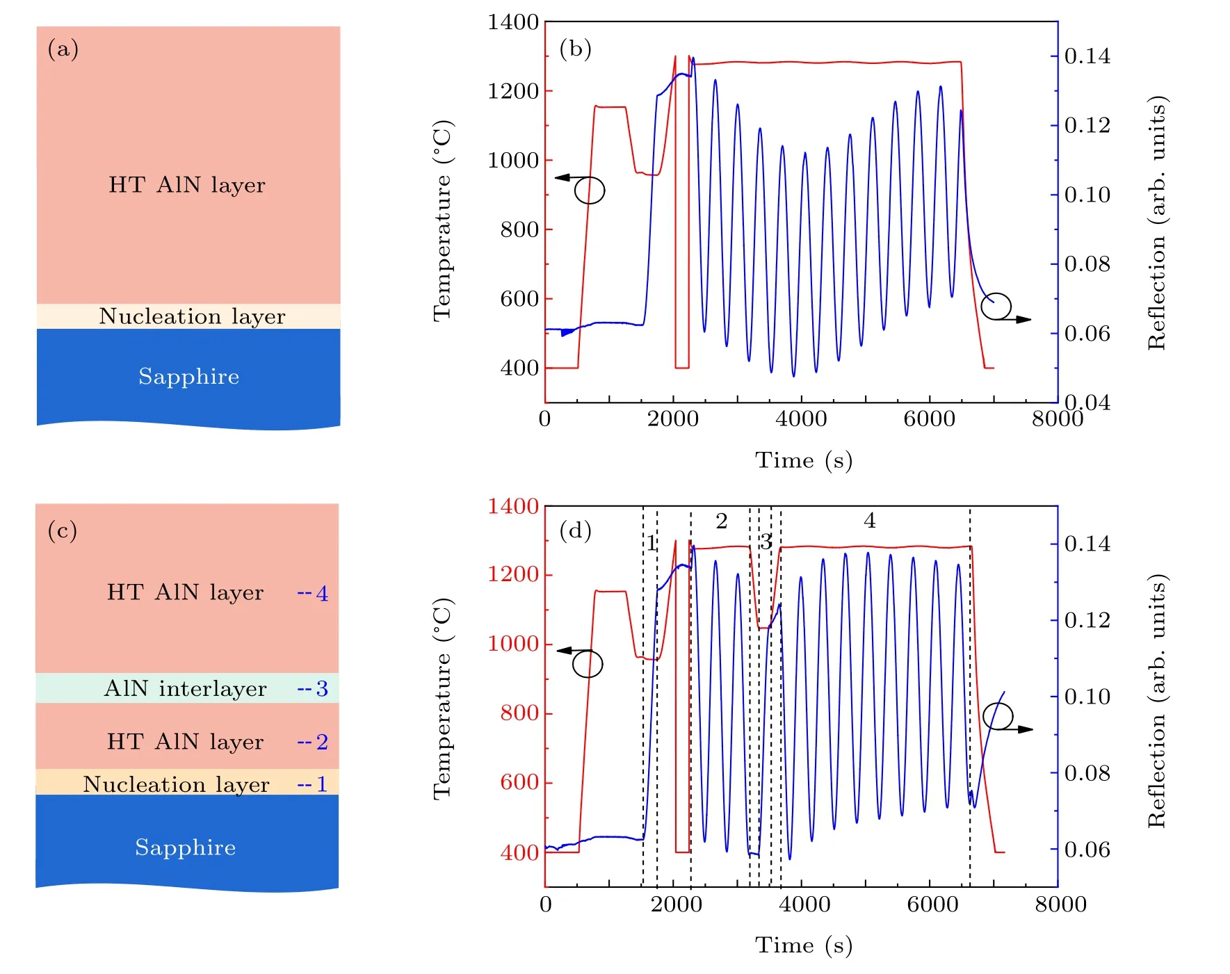
Fig. 1. (a) The epitaxy structure of the reference sample. (b) The in situ temperature and 405 nm reflection monitoring curves of the reference sample. (c)The epitaxy structure of the IL-AlN template and(d)the corresponding in situ temperature and 405 nm reflection monitoring curves.
Figure 1(a)shows the structure of the AlN template without AlN interlayer,which was designed as the reference sample. Thein situmonitoring curves of the reference sample are shown in Fig. 1(b). The HT-AlN was grown on the annealed nucleation layer without an interlayer. There is a total of 12.5 periods in thein situreflection curve and the curve decreases at first and then increases. It was found that the reflective intensity of the 6thperiod is the lowest among the 12.5 periods, which means the growth mode changes from three-dimensional to two-dimensional growth during the epitaxy of HT-AlN. The epitaxial structure of the AlN template with an interlayer(abbreviated as IL-AlN template)is shown in Fig. 1(c) and thein situmonitoring curves are shown in Fig. 1(d). Process 1 (about 220 s) and 3 (about 180 s) represent the growth of the AlN nucleation layer and AlN interlayer,respectively. Process 2(about 900 s)and 4(about 3000 s)represent the growth of HT-AlN.From Fig.1(d),it can be noted that there is a total of 12 periods in thein situreflection monitoring curve, and the growth of the interlayer is located at the first half of the 4thperiod. The results indicate that the interlayer is located at a height of about a 1/3 of the thickness of the AlN layer. A similar result can be obtained by analyzing the growth time. The intensity of the 4thperiod reflective curve drops sharply compared to that of the 3rdperiod,which indicates that three-dimensional island growth has occurred during the growth of the interlayer. After the growth of the AlN interlayer, the reflective intensity of the HT-AlN increases rapidly, which indicates that two-dimensional growth mode has occurred.

Fig.2. (a)and(b)The(0002)plane and(10-12)plane XRCs of the reference sample with/without 1700 °C annealing,respectively; (c)and(d)the(0002)plane and(10-12)plane XRCs of the IL-AlN template with/without 1700 °C annealing,respectively; (e)the Raman shift spectrum of the IL-AlN template before and after 1700 °C annealing. (f)The enlarged picture of AlN E2(high)peaks in(e).
The crystal quality of the as-grown AlN templates and annealed AlN templates was characterized by XRC. The results are shown in Figs. 2(a) to 2(d). After 1700°C annealing, the full width at half-maximum (FWHM) of the (10-12)plane XRC decreases evidently for both the reference sample and IL-AlN template. After annealing, the FWHM of the(10-12) plane XRC decreases from 971 arcsec to 292 arcsec for the IL-AlN template. Meanwhile, the FWHM of the(0002) plane XRC remains almost unchanged before and after annealing (110 arcsec and 138 arcsec). The results indicate that the dislocations were annihilated during the HTA process. According to the formula for calculating the dislocation density in Ref. [18], the calculated total dislocation density(TDD) of the annealed IL-AlN template is 5.1×108cm-2,which is one magnitude lower than that of the AlN before annealing (5.26×109cm-2). Furthermore, Raman measurement was taken to exhibit a change in the stress in the AlN layer. The Raman shift spectrum of the IL-AlN template before/after annealing is shown in Fig.2(e),and the peak of sapphire(418 cm-1)is taken as calibration.[21]Figure 2(f)is the enlarged picture of the AlN E2 (high) peak because the E2(high) peak of AlN is commonly used to calculate the stress in AlN.It was found that the E2(high)peak of AlN blueshifts after HTA,which means there is higher compressive stress in the annealed AlN layer than in the AlN without annealing.[22]The higher compressive stress proves the decrease in crystal boundary density and dislocation density in AlN.[18,22]The results indicate that the related physical phenomena are consistent with previous reports.[23,24]
There are two theories to explain the formation mechanism of the voids in HTA PVD-AlN.One is that the voids are formed by the coalescence of the crystal boundaries, and the other is that the voids are formed by the migration and annihilation of the dislocations.[18–20]In fact, the two theories are fundamentally the same, since the crystal boundaries are the locations of dislocation aggregation.[25,26]Consequently,the dislocations will annihilate and form voids at the crystal boundaries with a high degree of probability during the HTA.Once the dislocations around the crystal boundary have almost been annihilated, the crystal boundary will disappear, which can be described as the coalescence of the crystal boundaries.Based on the above mechanisms and thein situreflection curves, as shown in Fig. 1, it can be inferred that the voids will appear around the middle of the reference sample after HTA.For the HTA IL-AlN template,the voids are expected to appear at a height of 1/3 of the thickness of the AlN epitaxial layer above the AlN/sapphire interface. In order to confirm these inferences, the cross-sectional SEM images of the AlN templates with and without annealing are shown in Fig.3.
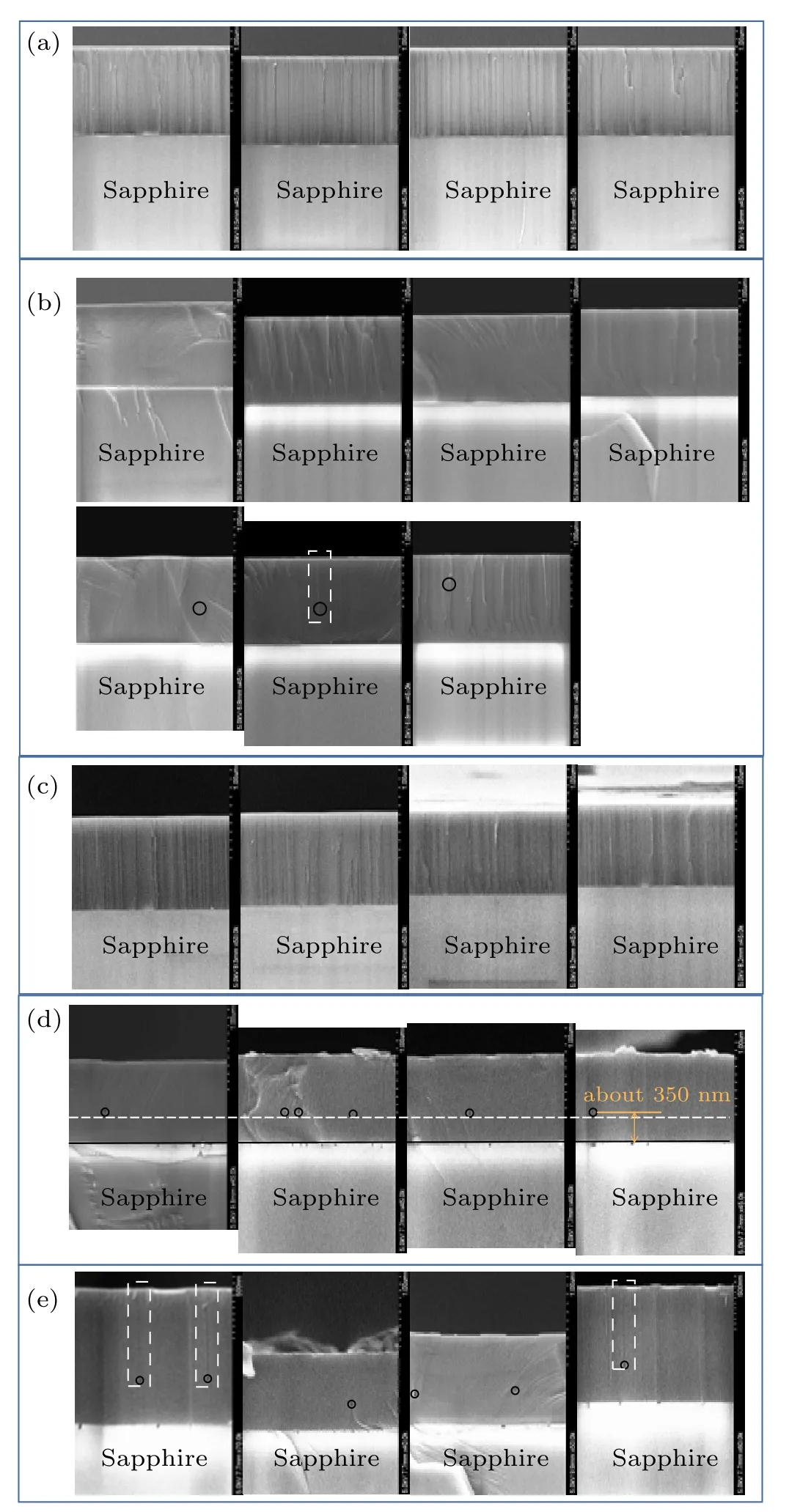
Fig.3. The cross-sectional SEM images at different locations of(a)the reference sample without annealing,(b)the annealed reference sample,(c)the IL-AlN template without annealing,(d)the annealed IL-AlN template with a magnification ratio of 45k and(e)the annealed IL-AlN template with a different magnification ratio. The voids are in the black circle and the channels are in the white-dashed rectangles.
Figure 3(a)shows the cross-sectional images of the reference sample at different locations without annealing. No void can be found in the AlN layer. The cross-sectional images of the annealed reference sample at different locations are shown in Fig.3(b). It was found that the density of the voids is low and the voids tend to form in the middle of the sample with a wide distribution range. The phenomena can be explained by the low intensity of thein situreflection curve during the middle stage of the AlN growth,as shown in Fig.1(b). As a comparison, the cross-sectional SEM images of the IL-AlN template with/without annealing at different locations are shown in Figs.3(c)–3(e). Figure 3(c)shows the cross-sectional SEM images of the IL-AlN template without annealing at different locations. It can be clearly confirmed that there is no void in the AlN layer before annealing. The four pictures in Fig.3(d)are the cross-sectional SEM images of the IL-AlN template with 1700°C annealing at the same magnification ratio of 45k.The SEM images are calibrated by the black line at the interface of the AlN layers and sapphire substrates, and the positions of the voids are marked by the white-dashed line,which is slightly lower than the voids. From Fig.3(d),it can be seen that the voids are located at almost the same level above the AlN/sapphire interface. According to the SEM results, the thickness of the AlN layer is about 1.1 μm,and the voids are located at a horizontal level that is about 350 nm higher than that at the AlN/sapphire interface. In addition to the fact that the interlayer is located at a height of about 1/3 of the thickness of the AlN layer above the AlN/sapphire interface, the voids could be considered to be formed around the interlayer. Moreover, the square voids beneath the AlN/sapphire interface are formed by the decomposition of sapphire according to a previous report.[27]Figure 3(e) shows the cross-sectional SEM results of the annealed IL-AlN template with different magnification ratios. It is estimated that the voids are located around the interlayer and the possibility of pollution can be excluded.

Fig. 4. The surface morphology of the AlN interlayer (a) before annealing and(b)after 1700 °C annealing for one hour.
In order to confirm the possible formation mechanism on the voids in the AlN layer, the surface morphology of the AlN interlayer has been characterized by AFM, as shown in Fig. 4(a). It was confirmed that the surface of the AlN interlayer consists of large island-like structures, which confirms the existence of a large number of crystal boundaries. After 1700°C annealing, the islands will coalesce, and there are many islands with regular edge shape on the step-like surface morphology (some of the step edges are marked by arrows),as shown in Fig.4(b). Based on the AFM results,it was confirmed that the voids are formed by the coalescence of the crystal boundaries. However,it should be noted that there are channels on some voids,as shown in the white-dashed rectangles in Figs.3(b)and 3(e).These channels connect the voids to the surface of the AlN templates. This phenomenon may provide another possibility that some voids may be formed by the decomposition of AlN.Further research is required to confirm this inference.
4. Conclusion and perspectives
Voids have been introduced around the AlN interlayer by annealing the AlN template with the AlN interlayer. The formation mechanism of the voids is mainly attributed to the coalescence of crystal boundaries, but some of the voids may be formed by the decomposition of AlN. Meanwhile,the dislocation density decreased to 5.10×108cm-2from 5.26×109cm-2. This work provides a potential method to introduce voids into AlN at a designated layer with a certain height, which improves the crystal quality of AlN. There are still some issues to be improved in further research work. For example,the density and volume of the voids should be further increased,and the voids should be introduced periodically into the AlN layer along with the growth orientation.
Acknowledgments
Project supported by the National Key Research and Development Program of China(Grant No.2017YFB0404100),the National Natural Science Foundation of China (Grant Nos. 61827813, 61974144, and 62004127), the Key Research Program of the Chinese Academy of Sciences(Grant No. XDPB22), the Key-Area Research and Development Program of Guangdong Province, China (Grant Nos. 2020B010169001 and 2020B010174003), and the Science and Technology Foundation of Shenzhen (Grant No.JSGG20191129114216474).
猜你喜欢
杂志排行

Chinese Physics B的其它文章
- Real non-Hermitian energy spectra without any symmetry
- Propagation and modulational instability of Rossby waves in stratified fluids
- Effect of observation time on source identification of diffusion in complex networks
- Topological phase transition in cavity optomechanical system with periodical modulation
- Practical security analysis of continuous-variable quantum key distribution with an unbalanced heterodyne detector
- Photon blockade in a cavity–atom optomechanical system