Heterogeneous integration of GaSb layer on(100)Si substrate by ion-slicing technique
2022-08-01RenJieLiu刘仁杰JiaJieLin林家杰ZhengHaoShen沈正皓JiaLiangSun孙嘉良TianGuiYou游天桂JinLi李进MinLiao廖敏andYiChunZhou周益春
Ren-Jie Liu(刘仁杰), Jia-Jie Lin(林家杰), Zheng-Hao Shen(沈正皓), Jia-Liang Sun(孙嘉良),Tian-Gui You(游天桂),§, Jin Li(李进), Min Liao(廖敏), and Yi-Chun Zhou(周益春)
1Key Laboratory of Low Dimensional Materials and Application Technology of Ministry of Education,School of Materials Science and Engineering,Xiangtan University,Xiangtan 411105,China
2Hunan Provincial Key Laboratory of Thin Film Materials and Devices,School of Materials Science and Engineering,Xiangtan University,Xiangtan 411105,China
3College of Information Science and Engineering,Jiaxing University,Jiaxing 314001,China
4State Key Laboratory of Functional Materials for Informatics,Shanghai Institute of Microsystem and Information Technology,Chinese Academy of Science(CAS),Shanghai 200050,China
5Beijing Semicore ZKX Electronics Equipment Co.,Ltd,Beijing 100000,China
Keywords: ion-slicing technique,heterogeneous integration,GaSbOI
1. Introduction
Among III–V compound semiconductors, the GaSb is a particularly significant semiconductor since its lattice parameter can be easily matched to various ternary and quaternary III–V compounds whose band gaps cover a wide range from~0.3 eV to 1.58 eV,e.g., 0.8 μm–4.3 μm.[1]Furthermore, it makes the detection of longer wavelengths(8 μm–14 μm)possible with intersubband absorption in the antimonide based superlattice. These have attracted huge attention in the development of GaSb applications in the fabrication of high-speed and microwave devices, infrared detectors, and long-wavelength lasers.[1–3]Additionally,the GaSb-based devices are a promising candidate for a variety of military and civil applications in long-wavelength regimes,such as infrared imaging sensors for missile and surveillance systems, fire detection, and monitoring environmental pollution.
However,owing to the difficulty in fabricating,the semiinsulating GaSb substrate is not available currently, which limits its widespread applications. Heteroepitaxial growth of GaSb-based devices on GaAs substrates and Si substrates as an integration strategy has attracted considerable attention due to the numerous advantages in optoelectronic devices that can be enabled, including monolithically integrated lasers, detectors, solar cells, and transistors.[3–7]Nevertheless, this integration strategy is challenged by the conjunction of large lattice and polarity mismatches, especially for the heteroepitaxial growth on Si substrate(13%lattice mismatch with GaSb).These large mismatches easily give rise to planar defects,the antiphase boundaries (APBs) and misfit dislocations in epitaxial layers, which can reduce the device performance and reliability. Fortunately, ion-slicing technique appears to conduce to the further development of heterogeneous integration between the mismatched materials. Ion-slicing technique was developed first by Bruel in 1995,and now it has been successfully applied to the mass production of Si-on-insulator wafers(SOI).[8]In the ion-slicing technique, the light elemental ion implantation followed by wafer bonding and annealing allows relatively thick layer to slice and transfer from a donor substrate to a host material without worrying about the physical mismatch in heteroepitaxial growth. During annealing,the vacancies are introduced by the ion implantation and light elemental ions precipitate into the formation of platelet defects in nanometer dimensions, which progressively grow by Ostwald ripening.[9,10]With the concentration of the implanted ions increasing in platelet defect, the platelet defect evolves and finally coalesce to form micro-cracks.[9]The further thermal evolution of the micro-cracks leads to the fracture phenomenon, including blistering or exfoliating on the surface.When a stiffener is intentionally bonded onto the wafer surface, the overall layer, parallel to the wafer surface, can be split.[11]Hence, the ion-slicing technique can not only avoid physically mismatching materials to achieve heterogeneous integration, but also directly peel from the single crystal substrate to produce high- quality single crystal films. Furthermore,one substrate can be transferred multiple times to reduce the cost,which is important especially for the expensive materials. This method has been extended to the area of compound semiconductors,such as Si-based InP,SiC,GaN,and Ga2O3,LiTbO3.[12–16]Some researches of the exfoliation or blistering behaviors of GaSb under different ion implantation conditions have been conducted,[17–19]but no report shows that the highquality GaSb layer has been transferred onto the Si substrate successfully by ion-slicing technique so far.
In this study,the splitting mechanism of GaSb is analyzed in detail. Combining direct wafer bonding, the GaSb layer is successfully transferred onto the Si/SiO2substrate to form high-quality GaSb-on-insulator(GaSbOI)structure.
2. Experimental details
The 350-μm-thick N-type (100) GaSb wafers having 2-inch(1 inch=2.54 cm)diameter were used in this study. The GaSb wafers were implanted by 75-keV H ions supplied from Nissin-implanter,respectively,with a fluence of 2×1016cm-2and 5×1016cm-2at room temperature.In order to avoid channeling effects,the 7°off the wafer normal was performed deliberately during the implantation process. After implantation,some of the GaSb wafers were cut into small samples for being characterized. Some of the samples implanted with 2×1016-cm-2and 5×1016-cm-2H ions were annealed at 200°C and 150°C with a constant flux of N2, respectively. The optical microscope (OM), Leica DM4000M, was used to characterize the surface morphologies of the samples. The strain variations under different annealing temperatures were characterized by x-ray diffraction(XRD)with Pilips X’Pert x-ray diffractometer. The cross-sectional transmission electron microscopy (XTEM), JEOL 2100F field-emission transmission electron microscope, was adopted to characterize the defects introduced by ion implantation. The quality of the different regions in sample was examined by selected area electron diffraction(SAED).Combined with direct wafer bonding,the GaSb layer was successfully transferred onto the Si/SiO2substrate. The surface topography was characterized by atomic force microscope (AFM) with Bruker Multimode 8. The structure of the GaSbOI substrate was characterized by crosssectional scanning electron microscopy (SEM) JEOL 7800F.The quality of the transferred GaSb layer after being annealed at different temperatures was examined by XRD and Raman excited by a 514.5-nm laser through using the Horiba Scientific LabRAM HR.
3. Results and discussion
In order to analyze the blistering behaviors, the GaSb samples implanted with 2×1016-cm-2and 5×1016-cm-2H ions are annealed at 200°C for 1 h. It is obvious that there is no change on the surface of sample implanted with 2×1016-cm-2H ions, while there are many bubbles and exfoliations on the surface of sample implanted with 5×1016-cm-2H ions as shown in Figs.1(a)and 1(b). The blistering efficiency depends on the extent of the damage produced by ion implantation because it affects the microstructure of the implanted sample. This microstructure is affected by the ion fluence.[20]The low ion fluence forms not only a small number of defects,but also the internal pressure of the defects which is not enough to overcome the facture energy of substrate,so no bubbles occur on the surface, which is regarded as a behavior of sample implanted with 2×1016-cm-2H ions. Owing to the nature of easy oxidation, the annealing temperature for GaSb must be lower. Therefore, the GaSb samples implanted with 5×1016-cm-2H ions are annealed at 150°C for 3 min and 1 h, respectively. As shown in Fig. 1(c), when the annealing time is 3 min,a large number of uniformly distributed bubbles appear on the surface. With the annealing time extending to 1 h, there is no significant increase in the volume of the bubbles,while some exfoliations occur on the surface as shown in Fig.1(d).During annealing,the defects need enough energy to migrate and coalesce together. Hence,for the GaSb implanted with 5×1016-cm-2H ions, the annealing at 150°C can meet the energy demand for the defect evolution to deform the surface causing blistering or exfoliation, which is necessary for the GaSb layer transfer.
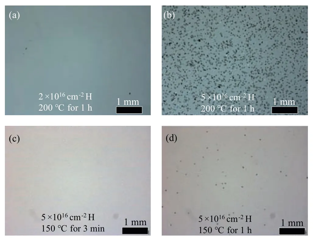
Fig. 1. OM image of GaSb implanted with (a) 2×1016-cm-2 H ions, (b)5×1016-cm-2 H ions after being annealed at 200 °C for 1 h,5×1016-cm-2 H ions after being annealed at 150 °C for(c)3 min and(d)1 h.
During annealing, the driving force of defect evolution is the strain introduced by the ion implantation. The XRD is used to analyze the strain variation of the GaSb sample implanted with 5×1016-cm-2H ions after being annealed at different temperatures. Figure 2(a)shows theω/2θXRD scans along the GaSb (004) reflections. Compared with the virgin GaSb, the implanted GaSb sample presents additional scattered intensity for angles lower than the Bragg angle,indicating that there is an out-of-plane tensile strain introduced by ion implantation.[21]As reported early , the most distant fringe from the Bragg angle corresponds to the maximum strain in the GaSb sample.[21]With the temperature increasing,the additional scattered intensity decreases gradually until it disappears completely at 130°C. It indicates that the increase in the annealing temperature promotes the evolution of defects,resulting in the release of strain. The 130°C corresponds to a defect transition temperature,at which the strain introduced by ion implantation is fully released. In order to analyze the defect formation, the XTEM is utilized to characterize the microstructure for the GaSb sample implanted with 5×1016-cm-2H ions after being annealed at 130°C.Figure 2(b)shows the cross-sectional TEM image and the inset displays the H ion distribution and displacement per atom(DPA)distribution simulated by SRIM 2008.[22]The DPA is commonly used to evaluate the degree of radiation damage to materials.It is obvious that the ion implantation gives rise to a damaged layer consisting of large density of defects in the GaSb sample as shown by the red dashed line. The damaged layer is 250-nm thick and 500-nm away from the surface. The maximum damage is around the upper boundary of damaged layer, while the peak of the H ion distribution is located in the middle of the damaged layer. Figure 2(c)shows the high-resolution TEM image for the damaged layer region in Fig. 2(b). Some platelet defects,parallel to the surface,appear in the damaged layer. Just like the H ion implantation into the Si substrate,the implanted H ions and some of the vacancies generated by the implantation coprecipitate during annealing and from two-dimensional circular objects named platelet defect.[10]The platelet defects serve as the precursors of the microcracks, which are essential for the layer splitting. Hence, the formation of platelet defects causes the strain to release, corresponding to the results of Fig.2(a). With the temperature increasing,the driving force of the evolution of platelet defects is the pressure inside the defects instead of the strain introduced by ion implantation. Figure 2(d) shows the SAED images corresponding to the three regions in Fig.2(b). The diffraction patterns in three regions show regular and bright spots rather than diffraction rings,which proves that the 5×1016-cm-2H ion implantation does not make the lattice amorphous in GaSb. However, the spots in region 1 are a little bigger than the spots in region 2,which means that in region 1 there are much heavier lattices disordered than in region 2. All the implanted ions go through region 1 to region 2. It is reasonable to think that the multiple collisions between the ions and lattice atoms in region 1 cause the much heavier lattice to disorder. Hence, the implantation condition of 5×1016-cm-2H ions is suitable to the splitting of the GaSb layer.

Fig. 2. (a) Patterns of ω/2θ XRD scan along GaSb (004) reflections for virgin GaSb and GaSb implanted with 5×1016-cm-2 H ions after being annealed at different temperatures;(b)cross-sectional TEM image of GaSb implanted with 5×1016-cm-2 H ions after being annealed at 130 °C;(c)high-resolution TEM image for the damaged layer in panel(b);(d)SAED images corresponding to the three regions in panel(b).
Based on the analysis of the splitting mechanism of GaSb,the process of GaSb layer transfer by ion-slicing technique is shown in Fig. 3. Firstly, the GaSb wafer is implanted with 5×1016-cm-2H ions at 75 keV. Then, the implanted GaSb wafer is bonded with a 4-inch SiO2/Si(100)substrate directly after the surface has been activated by O2plasma. The O2plasma activation can remove the contaminants and increase the density of the dangling bonds on the wafer surface,which is beneficial to achieving high bonding strength at low temperature. Subsequently, the bonding pair of GaSb/SiO2/Si (100)is annealed at 150°C for 1 h in a furnace with an N2atmosphere to achieve the GaSb layer transfer.

Fig.3. Flowchart of our scheme for GaSb layer transfer by ion-slicing technique.
Figure 4(a) shows the images of the bonding pair of of GaSb/SiO2/Si(100)after being annealed at 150°C for 1 h. It is obvious that the upper GaSb wafer is broken up into small pieces. With linear thermal expansion coefficients of Si and GaSb being 2.6×10⁻⁶C-1and 7.75×10⁻⁶C-1, there is a large thermal mismatch between Si and GaSb. During annealing,a huge thermal stress introduced by the large thermal mismatch exceeds the fracture energy of GaSb,causing the GaSb wafer to be broken. The annealing process needs to be further optimized to reduce the thermal stress, including reducing the rate of heating and cooling. After removing the pieces of GaSb wafer,the GaSb layer is transferred onto the SiO2/Si substrate to fabricate the GaSbOI substrate, which is shown in Fig.4(b). Owing to the huge thermal stress resulting from debonding,the GaSb layer in some region is not successfully transferred onto the SiO2/Si substrate.The surface topography of the GaSb is characterized by AFM as shown in Fig. 4(c).The scan covers an area of 5 μm×5 μm.The transferred GaSb layer has a high surface roughness of 27 nm, which should be polished to be sufficiently smooth for subsequent epitaxial growth. The GaSbOI substrate shows distinct three layers,including GaSb layer,SiO2layer,and Si substrate,respectively,as shown in Fig.4(d). The thickness of GaSb layer is around 630 nm,corresponding to the maximum peak of H ion distribution in Fig.2(b). Figure 4(e)shows a typical cross-sectional TEM image of GaSbOI, which reveals a sharp and smooth bonding interface between GaSb substrate and SiO2/Si substrate. The quality of the transferred GaSb layer is evaluated by high-angle annular dark field-STEM (HAADF-STEM) as shown in Fig. 4(f). In the HAADF-STEM image, the atoms of GaSb are arranged in regular lattice structure without any visible misfit dislocations, which proves that the GaSb layer has a perfect single-crystal structure.
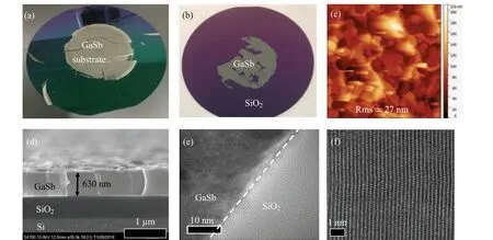
Fig.4. (a)Photo for GaSb/Si bonding pair after being annealed at 150 °C for 1 h;(b)photo of GaSb layer transferred on Si substrate;(c)AFM image for transferred GaSb layer;(d)SEM image of GaSbOI structure;(e)cross-sectional TEM image of GaSbOI;(f)HAADF-STEM image for transferred GaSb layer.
The quantitative characterization of the quality of the transferred GaSb layer is evaluated by x-ray rocking curve(XRC)measurement. The normalized(004)XRDs of the bulk GaSb substrate and the transferred GaSb layer before and after being annealed at 200°C are shown in Fig. 5(a). Obviously, an additional scattering peak appears to be lower than the Bragg angle of GaSb, while the peak disappears after being annealed at 200°C. Additionally, the full width at half maximum (FWHM) of the XRCs of the GaSb layer before and after being annealed remains constant, about 77 arcsec,which is slightly higher than that for the bulk GaSb substrate(20 arcsec). Therefore,it is reasonable to speculate that there are some defects in the transferred GaSb layer,which reduces the crystalline quality and cannot be recovered after being annealed at 200°C.The FWHMs of the XRCs of the GaSb layer before and after being annealed are significantly larger than that of virgin GaSb. The ion implantation will introduce a damaged layer containing large density of defects in the GaSb substrate as shown in Fig.2(b).Although the GaSb layer splitting occurs in the damaged layer,there are still many residual defects in the transferred GaSb layer. After being annealed at 200°C,only part of the defects recombin and disappear due to the restricted energy.Hence,these residual defects in the GaSb layer causes significantly larger FWHM of the XRCs even after being annealed at 200°C. In order to characterize the defects in the as-transferred GaSb layer,the Raman spectrum is utilized to analyze the components of the region near to the surface of the GaSb layer before and after being annealed at 200°C as shown in Fig.5(b). The GaSb layer is found to have typical first-order TO mode and LO mode before and after being annealed, and so is the virgin GaSb substrate, while an additional peak appears at around 155 cm-1for the GaSb before being annealed as shown by the black dashed line square.As reported early,during annealing,the segregation of Sb element easily happens to form a peak at about 155 cm-1in Raman scattering spectrum.[23]After being annealed at 200°C,it is reasonable to believe that the atoms near to the surface of GaSb layer are rearranged to recover the crystalline structure.Hence, the annealing at 200°C is essential for GaSb layer to improve its crystalline structure.

Fig.5. (a)Normalized(004)XRCs for bulk GaSb substrate and transferred GaSb layer before and after being annealed at 200 °C; (b) normalized Raman spectrum for virgin GaSb and transferred GaSb layer before and after being annealed at 200 °C.
4. Conclusions and perspectives
In this work, we analyzed the blistering and exfoliation behaviors of GaSb after H ion implantation and confirm the suitable ion implantation fluence of 5×1016-cm-2H ions for GaSb layer transfer. During annealing, the strain introduced by the H ion implantation as the driving force accelerates the coprecipitation of the implanted H ions and some of the vacancies generated by the implantation to form the platelet defect. With the temperature increasing, the pressure inside the platelet defects,instead of the strain introduced by ion implantation,drives the platelet defects to evolve. Based on the analysis of the splitting mechanism of GaSb,the monolithic integration of high-quality GaSb layer with SiO2/Si substrate is successfully achieved by the ion-slicing technique. The crystalline quality of the GaSb layer can be further improved by annealing at 200°C.The high-quality heterogeneous integration of GaSb on the SiO2/Si substrate promises to become a novel platform for infrared applications.
Acknowledgements
Project supported by the National Key Research and Development Program of China (Grant No. 2017YFE0131300),the National Natural Science Foundation of China (Grant Nos.U1732268,61874128,11622545,61851406,11705262,61875220, and 61804157), the Frontier Science Key Program of Chinese Academy of Sciences(Grant Nos.QYZDYSSW-JSC032 and ZDBS-LY-JSC009), the Chinese–Austrian Cooperative Research and Development Project (Grant No. GJHZ201950), the Shanghai Science and Technology Innovation Action Plan Program, China (Grant No. 17511106202), the Program of Shanghai Academic Research Leader, China (Grant No. 19XD1404600), the Shanghai Youth Top Talent Program, Shanghai Sailing Program,China (Grant Nos. 19YF1456200 and 19YF1456400), the K.C. Wong Education Foundation, China (Grant No. GJTD-2019-11), and the NCBiR within the Polish–China (Grant No.WPC/130/NIR-Si/2018).
猜你喜欢
杂志排行

Chinese Physics B的其它文章
- Real non-Hermitian energy spectra without any symmetry
- Propagation and modulational instability of Rossby waves in stratified fluids
- Effect of observation time on source identification of diffusion in complex networks
- Topological phase transition in cavity optomechanical system with periodical modulation
- Practical security analysis of continuous-variable quantum key distribution with an unbalanced heterodyne detector
- Photon blockade in a cavity–atom optomechanical system