Enhancing performance of GaN-based LDs by using GaN/InGaN asymmetric lower waveguide layers
2022-08-01WenJieWang王文杰MingLeLiao廖明乐JunYuan袁浚SiYuanLuo罗思源andFengHuang黄锋
Wen-Jie Wang(王文杰), Ming-Le Liao(廖明乐), Jun Yuan(袁浚),Si-Yuan Luo(罗思源), and Feng Huang(黄锋)
1Microsystem and Terahertz Research Center,China Academy of Engineering Physics,Chengdu 610200,China
2Institute of Electronic Engineering,China Academy of Engineering Physics,Mianyang 621999,China
Keywords: asymmetric waveguide structure,InGaN multiple quantum wells,optical absorption loss,optical
1. Introduction
Nitride materials are ideal materials for semiconductor lasers in the ultraviolettovisible spectrum range. With the advantages of small size, high efficiency, long life, and fast response speed, GaN-based semiconductor laser is widely used in laser display, laser lighting, underwater communication, biomedicine, and other civil and military fields.[1–8]In particular, the GaN-based violet laser diodes (LDs) have attracted attention as a new laser source for high-density optical disk storage.[9,10]To realize such applications,high power GaN LD is significantly important. However, the electrooptical power conversion efficiency of commercial GaN-based laser diodes is still less than 40%. The structural design and material growth of GaN-based violet LDs have been studied extensively in the past. But achieving ultra-high performance of GaN-based violet LDs is still a big challenge. There remain some problems to be solved further in the realization of high power GaN LD, such as high total optical loss and optical field leakage. Many methods have been proposed to suppress the total optical loss and improve the optical field distribution for GaN-based violet LDs,such as complex upper waveguide,[11–13]undoped thickoptical-waveguide (TOW) layer,[14,15]and the nanoporous GaN cladding layers.[16]These complex structures with undoped InGaN wave guides are difficult to realize the high quality epitaxy on a quantum well structure, especially near a p-AlGaN electron barrier layer with high doping concentration.
At the same time,by increasing the thickness and refractive index of upper waveguide layer, the optical field distribution gradually moves into the N-type region,so that optical absorption loss is reduced and optical field distribution in Pregion is improved, which brings higher output power. However, when the optical field center is in quantum well region,how to further adjust optical field distribution and reduce optical absorption loss to improve the output power is not covered in the existing literature. Comparing with the traditional LD structure proposed by Nakamuraet al.,[17,18]the optical characteristics,especially optical field distribution,can be improved by using an asymmetric quantum wells with a thick last quantum barrier.[19]To solve this problem,an asymmetric InGaN quantum well LD with the optical field center in the quantum well region, is selected as a research object in this work. The influence of GaN/InGaN lower waveguide layer on the photoelectric performance of GaN-based violet LDs is investigated numerically by using the PIC3D software.The influence of InGaN-IL parameters on the optical absorption loss and optical field distribution are clarified by designing a composite GaN/InGaN lower waveguide layer,so as to explore the ways to further improve the output power of asymmetric quantum wells LDs.
2. Device structure and simulation setup
The schematic diagram of asymmetric quantum well violet GaN-based LD with composite GaN/InGaN asymmetric lower waveguide structure is shown in Fig. 1, where the thickness and doping concentration of each layer are indicated. The violet GaN-based LD consists of a 1-μm thick Si-doped n-type GaN layer, a 1-μm thick Si-doped ntype Al0.08Ga0.92N cladding layer (n-CL), a composite lower waveguide layer(LWG)which is comprised of a 100-nm thick Si-doped n-type GaN layer and an InGaN-IL,a multiple quantum well (MQW) active area, a 20-nm thick Mg-doped ptype Al0.2Ga0.8N electron blocking layer (EBL), a 100-nm thick GaN upper waveguide layer (UWG), a 500-nm thick p-type Al0.07Ga0.93N cladding layer (p-CL), an 80-nm thick Mg-doped p-type GaN layer, and a 20-nm thick Mg-doped p++-type GaN contact layer. The active region consists of three period unintentionally-doped In0.15Ga0.85N/InGaN multiple quantum wells(MQWs).The InGaN barrier layer has the indium content changing from 4%to 1%in the upward direction of the substrate. Compared with the conventional threeperiod 3-nm thick InGaN/15-nm thick GaN quantum wells,the asymmetric quantum well can effectively improve the laser performance,especially increase the thickness of the last barrier layer.[19]In order to keep the thickness of the asymmetric quantum well consistent with the thickness of the conventional three-period-thick MQWs, the thickness of the well layer of the asymmetric quantum well is 3 nm,the same as that of the conventional quantum well, and the thickness of the last barrier layer is increased to make the center of optical field located in the MQW region and improve the optical field distribution. The thickness for each of the first three barrier layers is set to be 5 nm, and the thickness of the last barrier layer is set to be 45 nm, so that the optical field can be concentrated in the quantum well region. The cladding layer thickness n-CL is set to be 1 μm in order to better confine the light within the quantum well and waveguide layer. Thicker n-AlGaN layer is unnecessary and will increase the absorption loss.The optical and electrical performance of GaN-based LDs with GaN/InxGa1-xN asymmetric lower waveguide layers of different thicknesses or indium contents are investigated respectively. The thickness values of n-InGaN insertion layers are different, ranging from 0 nm to 600 nm, with the indium content being 0.02. On the other hand, the indium content of n-InGaN insertion layer varies from 0 to 0.07,with the thickness being 300 nm.
In this work, the optical and electrical characteristics of these LD structures are theoretically simulated by the Crosslight Device Simulation Software (PIC3D, Crosslight Software Inc.). The PIC3D is designed to simulate the operation of GaN-based laser diode in three-dimensional space by self-consistently solving Poisson’s equation and current continuity equation through using the finite element method. In such a calculation, both the p-type electrode and n-type electrode are set to be of ideal Ohmic contact. The cavity lengths and ridge widths of these GaN-based lasers are all 800 μm and 2 μm,respectively. The P-electrode covers the ridge area and the N-electrode covers the entire underside.The screening factor is set to be 0.25,[20]and the band offset(ΔEc/ΔEg)is set to be 0.67.[21]Meanwhile,for the n-type layer and the p-type layer, their absorption coefficients are set to be 5 cm-1and 50 cm-1,[22]respectively, except for the heavily Mg-doped GaN contact layer, whose absorption coefficient is taken as 100 cm1. The reflectivity values of both front cavity surface and rear cavity surface are both set to be 0.19. Moreover,the refractive index values of AlxGa1-xN and InxGa1-xN are calculated from the refractive index formulas.[23–26]For the violet LDs with a lasing wavelength of around 416 nm, the refractive index values of InN, GaN and AlN are set to be 3.4167,2.5067, and 2.0767, respectively. The refractive index values of InxGa1-xN and AlxGa1-xN are calculated using an approximate method as follows:

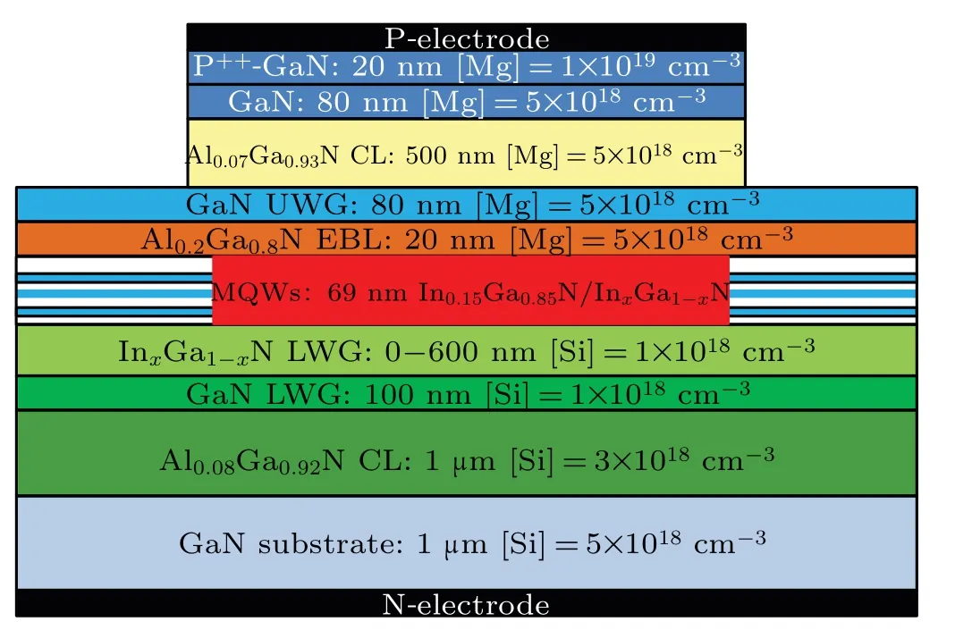
Fig. 1. Schematic diagram of device for asymmetric quantum well GaNbased violet LD with composite GaN/InGaN asymmetric lower waveguide structure.
3. Results and discussion
3.1. Effect of thickness of InGaN insertion layer
At first,the influence of InGaN-IL on the emission properties of violet LDs is investigated by simulation when the thickness value varies from 0 nm to 600 nm, with the indium content maintained at 2%. The curves of output power and voltageversusinjection current for various values of In0.02Ga0.98N insertion layer thickness are shown in Fig. 2.According to the output power–current curve, the slope efficiency of layer is calculated and its variation with thickness is shown in the insert of Fig.2(b),indicating that the slope efficiency is much higher than that in Refs. [11,12], and slightly lower than that in Ref.[13]. The dependence of threshold current and output power(under an injection current of 160 mA)on InGaN insertion thickness as shown in Fig.3.
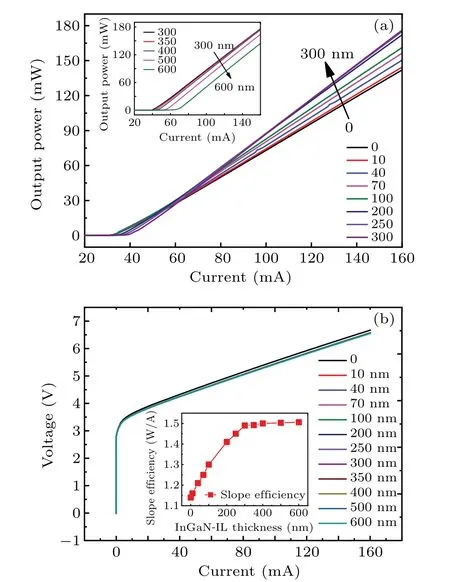
Fig.2. Curves of(a)output power versus injection current when thickness of In0.02Ga0.98N insertion layer varies from 0 nm to 600 nm,and(b)curves of voltage versus injection current for violet LDs,with inserts showing slope efficiencies.

Fig. 3. The output power and threshold current versus thickness of In0.02Ga0.98N-IL for violet LDs.
It is found that the threshold current remains first at 38.2 mA when the thickness of InGaN-IL rises from 0 nm to 100 nm, and then markedly increases to 74.4 mA with the further increase of InGaN-IL thickness. Meanwhile, the output power reaches a maximum value of 176.13 mW when the InGaN-LWG thickness increases to 300 nm, which is 24%higher than that of the basic structure with 142 mW, and then decreases sharply when the thickness increases to over 300 nm. It demonstrates that for violet LDs, the composite GaN/In0.02Ga0.98N waveguide with In0.02Ga0.98N insertion thickness less than 600 nm has better performance than GaN waveguide,and the optimal thickness is 300 nm. In addition,the current–voltage curve is basically unchanged, indicating that the increase of InGaN-IL thickness does not significantly increase the resistance.
In fact, the threshold current and the output power are mainly influenced by the optical confinement properties and optical field distribution.[27]Therefore, the influence of InGaN-IL thickness on the optical performance of GaN-based violet LDs will be discussed in detail below.

Fig.4. Curves of(a)optical confinement factor and total optical loss and(b)center of optical field offset and FWHM versus thickness of In0.02Ga0.98NIL for violet LDs,with insert showing optical field distribution and dashed lines denoting InGaN-IL position.
The data of optical properties reflecting optical field distribution are shown in Fig. 4, where the thickness of InGaNIL rises from 0 nm to 600 nm. In Fig. 4(a), the optical confinement factor (OCF) increases slightly from 2.4% to 2.56% when the thickness of InGaN-IL increases from 0 nm to 70 nm. Meanwhile, the total optical loss (TOL) decreases from 8.73 cm-1to 6.46 cm-1with the thickness of InGaNIL increasing. It indicates that the increasing of InGaN-IL thickness can reduce optical loss and a little enhance the confinement factor,thereby will better restricting the optical field.Therefore,the performance of violet LDs can be improved due to the decrease of TOL and increase of OCF.Simultaneously,it can be seen that with the increase of the IL layer thickness in Fig.4(a),the optical field concentrates more inside the InGaN-IL layer. However,the optical field peak deviates from the quantum wells. Even if more optical fields are distributed inside the InGaN-IL layer, the optical absorption loss further decreases, but the OCF may be reduced by shifting the peak position of the optical field.This is consistent with the trend of OCF in Fig.4(a)as the thickness of the barrier layer changes.Therefore,with the increase of the IL layer thickness,the peak position of the optical field moves from the MQW region to the n-type region,and the optical confinement factor slowly grows to a maximum value and then decreases rapidly. Meanwhile,the mode gain is the product of OCF and material gain. When the thickness exceeds 100 nm,the peak gain decreases gradually,confirming that the optical field gradually enters into the InGaN-IL layer,which is not conducive to OCF.The decrease of mode gain leads the threshold current to increase,which is consistent with the change trend of OCF in Fig.4(a).
Furthermore,the more details of optical field distribution are shown in Fig.4(b). The center of optical field(COF)offset is used to describe the position of the optical field center relative to the quantum well region. The value represents the depth from the peak position of the optical field to the InGaNIL.Most of optical field moves far away from p-type area with the thickness of InGaN-IL increasing,thus reducing TOL due to the smaller absorption coefficient in n-type area. In addition, the center of optical field (COF) offset shifts slowly from quantum well region to the InGaN-IL and full width at half maximum (FWHM) of the optical field decreases from 0.32 μm to 0.29 μm when the thickness rises from 0 nm to 100 nm. It demonstrates that the optical field is better compressed and thus optical field is confined more near the MQWs region. As the InGaN-IL is inserted, the difference in refractive index between InGaN-IL and AlGaN cladding increases,and the optical field is far from the P-type region and better compressed into the InGaN-IL close to the quantum well region,thus reducing the TOL and slightly increasing the OCF.However, when the InGaN-IL thickness exceeds 100 nm, the optical field center gradually deepens into the InGaN waveguide layer. At the same time,the FWHM gradually increases,and the OCF decreases due to serious downward leakage of the optical field. The reduction of TOL can offset the adverse effects caused by the optical field leakage, so that the output power reaches a maximum value when the thickness of the InGaN-IL is 300 nm.Moreover,after the insertion layer thickness reaches to over 300 nm,a small reduction in TOL is still not enough to slow down the output power decline caused by optical field leakage. On the other hand,the band structure of LD is basically unchanged when the insertion layer thickness increase to 300 nm, and the percentage of electron leakage current(PELC)decrease within 1%,indicating that the InGaN insertion layer thickness has little influence on the electrical performance of this LD,which is consistent with the current–voltage curve in Fig.2(b).
3.2. Effect of indium content of InGaN insertion layer
As mentioned above, the LD with an optical light field center in the quantum well region can increase the output power by 24% by inserting a 300-nm thick InGaN-IL. However,it has not been determined whether the output power can be further improved. Therefore, based on the 300-nm thick insertion layer,we further explore the power improvement potential by changing the indium content of the InGaN-IL.
Figure 5 shows that when the indium content in InGaNIL increases from 0 to 0.07, the threshold current increases from 40.1 mA to 55.2 mA.Meanwhile,when the indium content of InGaN-IL increases from 0 to 0.04, the output optical power first increases from 169 mW to 178.5 mW, which is 25.7%in enhancement with respect to the reference structure of asymmetric GaN waveguide LD.Compared with the effect of InGaN-IL thickness, the effect of indium content change on LD output power and threshold current are relatively small.When the indium content increases from 2%to 4%,the output power only increases by 2 mW and the increment ratio is less than 1.2%.

Fig.5.Output power and threshold current versus indium content of InGaNIL for violet LD.
Figure 6(a)shows that most of optical field leaks into the InGaN-IL when the indium content increases from 0 to 0.07.However, vast majority of optical field is concentrated in the GaN/InGaN LWG when the indium content is more than or equal to 0.04. Figure 6(b)shows that the center of optical field decreases abrupt from 2.35 μm to 2.26 μm with the indium content increasing and then reaches a constant at 2.26 mm when the indium content is more than 0.04. In addition, figure 6(b)also shows that the FWHM of optical field decreases from 0.41 μm to 0.28 μm when the indium content increases from 0 to 0.07,indicating that most of optical field moves far from MQW region and concentrates when the indium content is more than 0.04. It demonstrates that optical field leakage is enhanced due to the decrease of optical confinement caused by a large refractive index of GaN/InGaN LWG,thus threshold current increases obviously.

Fig. 6. (a) Optical field distributions for various indium contents, and (b)center of optical field and FWHM versus indium content of InGaN-IL for violet LD,with red dotted line denoting interface between InGaN-IL layer and the MQW.
Meanwhile,the trend of TOL and OCF changing with indium content in Fig. 7 also confirm the above statement and discussion. The TOL decreases rapidly, and moderates when the indium content is greater than or equal to 0.04. The reason is that as the center of the optical field gradually deepens into the InGaN-IL and is fixed at 2.26 μm,the proportion of the optical field with a low optical absorption coefficient in the composite waveguide layer and the quantum well region gradually increases,especially in the InGaN-IL.With the gradual increase of indium content,the rapid decrease of TOL can compensate for the adverse effects caused by the decrease of OCF,so that the LD output power reaches a maximum value when the indium content of InGaN-IL is 0.04. Similarly, the electrical properties of LD based on the GaN/InGaN composite lower waveguide layer structure show that the variation of indium content has a weak influence on the fluctuation of electron current leakage,and the fluctuation range is within 1.5%.

Fig.7. Optical confinement factor and total optical loss versus indium content of InGaN-IL for violet LD.

Fig.8. (a)Electron concentrations and(b)hole concentrations varying with position at 160 mA forward current for three samples.
In addition,the influence of the thickness and the indium composition of InGaN-IL on the electron and hole concentration are analyzed,and the results are given in Fig.8,showing that the electron and hole concentration in the quantum well increase slightly with the change of the thickness and composition, while In4-300 increases more. However, the variation of InGaN-IL thickness does not significantly change the energy band,especially the electron barrier layer interface. The band diagram shows that the thickness and the indium composition of InGaN-IL have slight effects on the effective potential barrier height of electrons and holes. ΔEcand ΔEvare around 192.3 meV and 193.7 meV, respectively, which is also confirmed in the PLEC diagram. When the indium component of InGaN-IL is high,a potential well will be formed between the GaN low waveguide layer and the first quantum barrier layer as indicated in Fig.9. In this case,the carriers may converge and recombine in the potential well.As mentioned in Ref.[28],the calculation results of recombination rate show that the carrier in InGaN-IL increases with indium content increasing. Since this part of the carrier does not contribute to oscillation,it results in low injection ratio and waste of carriers. Therefore,when the indium content of InGaN-IL layer is greater than 4%,the decrease of current injection ratio is also the cause of LD deterioration. It is suggested that using GaN/InGaN instead of GaN as LWG can improve the performance of LD,but the indium content should be kept at a relatively low level.Therefore,when a 300-nm thick In0.04Ga0.96N insertion layer is used, the laser output power is improved by 25.7% compared with the LD reference structure of the symmetric GaN waveguide layer.

Fig.9. (a)Energy band diagram of conduction band and(b)valence band,with InGaN-IL thickness being 300 nm and injection current being 160 mA.
4. Conclusions
In this work,the approach to improving the output power of violet GaN-based LD with the optical field centered in the quantum well region is proved by using asymmetric GaN/InGaN composite lower waveguide layer. Compared with the indium content of InGaN-IL,the thickness of InGaNIL is a decisive factor for improving the laser performance.The maximum output power of the laser reaches 178.5 mW,when the thickness of InGaN-IL is 300 nm and the indium content is 0.04. Further theoretical analysis indicates that the thickness and indium content of InGaN-IL are both beneficial to pushing the optical field towards the InGaN lower waveguide layer and greatly reducing the total optical loss, which makes up for the negative effect of the reduction of optical confinement factor, thereby improving the performances of GaN-based violet LDs.
Acknowledgements
Project supported by the National Natural Science Foundation of China (Grant Nos. 62004180 and 61805218), the Science Challenge Project, China (Grant No. TZ2016003-2-1), and the National Key Research and Development Program of China (Grant Nos. 2017YFB0403100 and 2017YFB0403103).
猜你喜欢
杂志排行

Chinese Physics B的其它文章
- Real non-Hermitian energy spectra without any symmetry
- Propagation and modulational instability of Rossby waves in stratified fluids
- Effect of observation time on source identification of diffusion in complex networks
- Topological phase transition in cavity optomechanical system with periodical modulation
- Practical security analysis of continuous-variable quantum key distribution with an unbalanced heterodyne detector
- Photon blockade in a cavity–atom optomechanical system