Combined effects of cycling endurance and total ionizing dose on floating gate memory cells
2022-05-16SiDeSong宋思德GuoZhuLiu刘国柱QiHe贺琪XiangGu顾祥GenShenHong洪根深andJianWeiWu吴建伟
Si-De Song(宋思德), Guo-Zhu Liu(刘国柱), Qi He(贺琪), Xiang Gu(顾祥),Gen-Shen Hong(洪根深), and Jian-Wei Wu(吴建伟)
The 58th Institution of Electronic Science and Technology Group Corporation of China,Wuxi 214000,China
Keywords: radiation,floating gate,threshold voltage,recombination
1. Introduction
Despite the rapid growth of new emerging alternative memories, such as the ferroelectric random access memory (FeRAM),[1–3]the magnetic random access memory (MRAM),[4,5]the phase change random access memory (PCRAM),[6,7]and the resistive random access memory (RRAM),[8,9]the flash memory still dominates the nonvolatile memory market due to its high reliability,high density,and low cost. For the electrical and electronic systems based on floating gate memories in aerospace technology,the effect of total ionizing dose(TID)and single event effect(SEE)remain big challenges.[10–13]In order to guarantee the reliability and performance of these floating gate(FG)memory incorporated systems, the fundamental mechanisms of TID and SEE on the FG memories need further exploring.
There have been several studies[10,14]of modeling the radiation response of FG memories, including mainly the following three mechanisms: (i) holes injected into the FG, (ii)holes trapped in the oxide,and(iii)electron emitted from the FG. These studies describe mainly the TID induced threshold voltage shift in floating gate memories, but not the radiation effects on device parameters such as leakage,or transconductance, or breakdown . Moreover, in real space-flight missions, the flash memories are subjected to both TID and cycling(programmed and erased,P/E)stress,and the reports on combined effects of cycling endurance and radiation on floating gate memories are quite few. So,it would be valuable and meaningful to have an in-depth study on the interaction between cycling stress and radiation to analyze the degradation mechanism and also to design radiation hardened FG memories.
In this study, the combined effects of cycling endurance and radiation on floating gate memory cell are emphasized.We find that an appropriate magnitude of cycling stress on flash cells before radiation can mitigate the threshold voltage shift in response to Co-60γ-ray irradiation. Both the programmed state and erased state with prior cycling stress exhibit more severe transconductance degradation than without cycling in advance; Radiation is more likely to set up the interface generation in programmed state than in erased state.
2. Experiment and devices
The FG memory cell tested in this work,also named 2TFlash,was fabricated based on the embedded p-Flash technology.The structure is displayed in Fig.1,a typical 2T-Flash cell consisted of two transistors, a select transistor, and a floating gate transistor. The flash cell operation included the program,erase and read. The program operation was to move electrons into the FG (programmed state), while the erasing operation was to remove the electrons out of the FG(erased state),then the state of the flash cell could be sensed or read by measuring the threshold voltage. In this work,the programmed state and erased state of the flash cells in response to radiation are studied in detail.
The flash cells were bound to a DIP20 ceramic dual-inline package,and all the devices under test(DUT)were classified into four conditions prior to irradiation,i.e., the programmed state with prior cycling stress (group 1), the programmed state without prior cycling stress (group 2), the erased state with prior cycling stress(group 3),and the erased state without prior cycling stress(group 4). The devices were irradiated by Co-60γ-ray source under normal incidence and at a constant dose rate of 50 rad (Si/s), the total dose is set to be 50 krad and 100 krad separately, all the terminals in the radiation process were grounded. After the specified total dose of radiation is reached,an electrical parameter test is performed. The electrical characteristics of the 2T-flash memory cells were measured with KEYSIGHT B1500 semiconductor device analyzer.
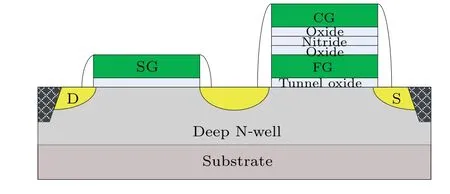
Fig.1. Typical structure of 2T-flash memory cell.
3. Results and discussion
The electrical characteristics in group 1 and group 2 devices are shown in Fig.2.It is observed that both the threshold voltage and the threshold transconductance in group 1 devices change only slightly before and after 2000 times P/E cycles,according to which we assume that the initial states of group 1 are“similar”to those of group 2 devices.
While after irradiation,the difference in threshold voltage shift between two groups is significant. The threshold voltage shifts of devices in group 1 are all 0.8 V for 50 krad(Si)and 2.1 V for 100 krad(Si)respectively,while those in group 2 devices are 2.3 V for 50 krad(Si)and 3.6 V for 100 krad(Si),respectively(see Figs.2(a)and 2(b)). In addition,the transconductance curves in both groups shift toward negative values and the peak value decrease,which is an indication of reduced electrons on the FG and increased interface state density, respectively. It is also noted that the conductance degradation in group 1 is more severe than in group 2, which we assume is the result of prior P/E cycling stress.The significant difference in threshold voltage shift is illustrated as follows.
The threshold voltage(Vth)versustotal doseγis quantitatively described in the following equation:[15]

whereγis the total dose,Vth(0)is the threshold voltage before irradiation,Vth(∞) is the saturation value, andAis the decay constant.
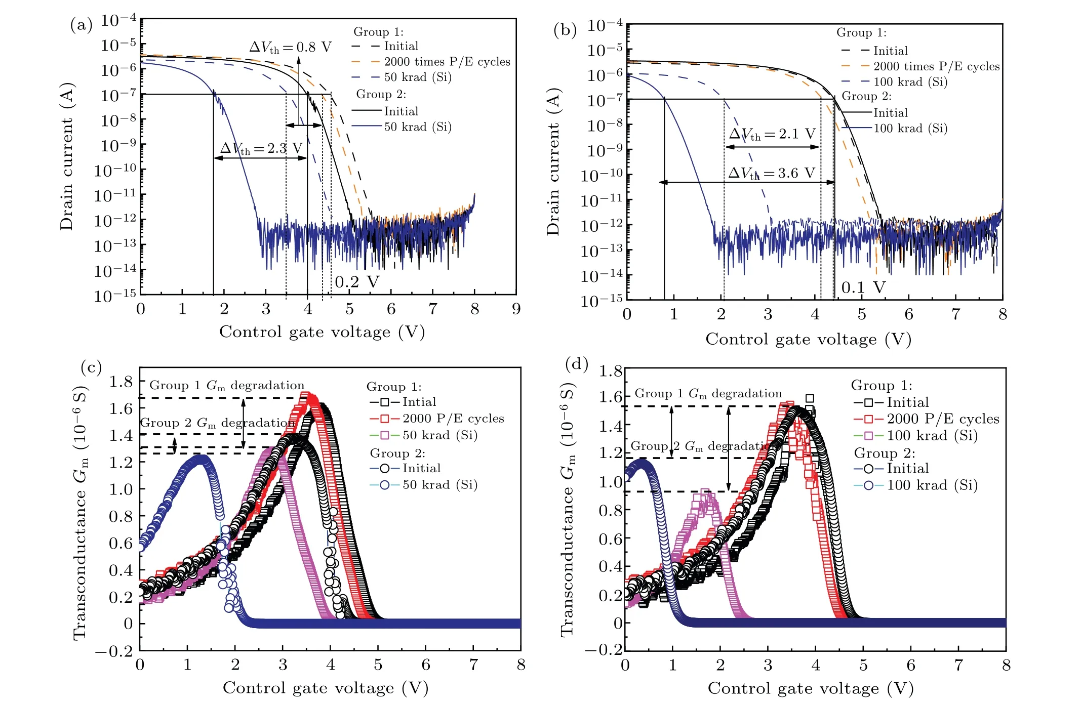
Fig.2. Electrical characteristics of programmed flash cell before and after TID,showing[(a)and(b)]transfer curves,and[(c)and(d)]transconductance curves.
As mentioned above, the initial states of group 1 and group 2 devices are“similar”in terms of initial threshold voltage and interface state density, while their responses to TID are quite different. According to Eq.(1),the threshold voltage after radiation is dependent on the initial threshold voltage,the total dose of radiation and the decay constant,so the threshold voltage shift difference may origin from the decay constant,which is closely related to the material properties and process technology,and also more likely to the prior P/E cycling stress.As is well known,the P/E cycling endurance leaves the tunnel oxide in high electrical stress,which may lead the oxide trap to generate and interface trap to generate. In our case,the interface trap after stress is negligible,so we assume that the large difference may be caused by the oxide trap. The schematic diagram of programmed flash cell in response to radiation is depictured in Fig.3.
As illustrated in Fig. 3, there are a majority of electrons stored on the floating gate at the programmed state, forming strong electric field in the surrounding oxide layers. When irradiated, the following three main processes may cause the electrons to lose from the floating gate: (I) photoemission(electrons on the floating gate absorb enough energy from the photons and overcome the barrier(>3.2 eV)of the surrounding dielectric layer); (II) the hole hopping and trapping (the radiation induced holes in the oxide layer transport through local state and some are trapped near the SiO2/floating gate interface); (III) the hole injection (Some holes may escape from the trapping process and directly enter into the floating gate and recombine with the electron localized). Thus, the threshold voltage shift(ΔVth)after irradiation can be expressed below:[11]
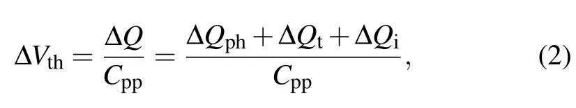
whereCppis the floating gate to control gate capacitance,ΔQis the total electron loss from floating gate,ΔQph,ΔQt,andQiare the electrons lost due to photoemission,hole trapping,and hole injection,respectively,with all normalized into the value per unit area.

Fig.3. Programmed flash cell in response to Co-60 γ-ray radiation.
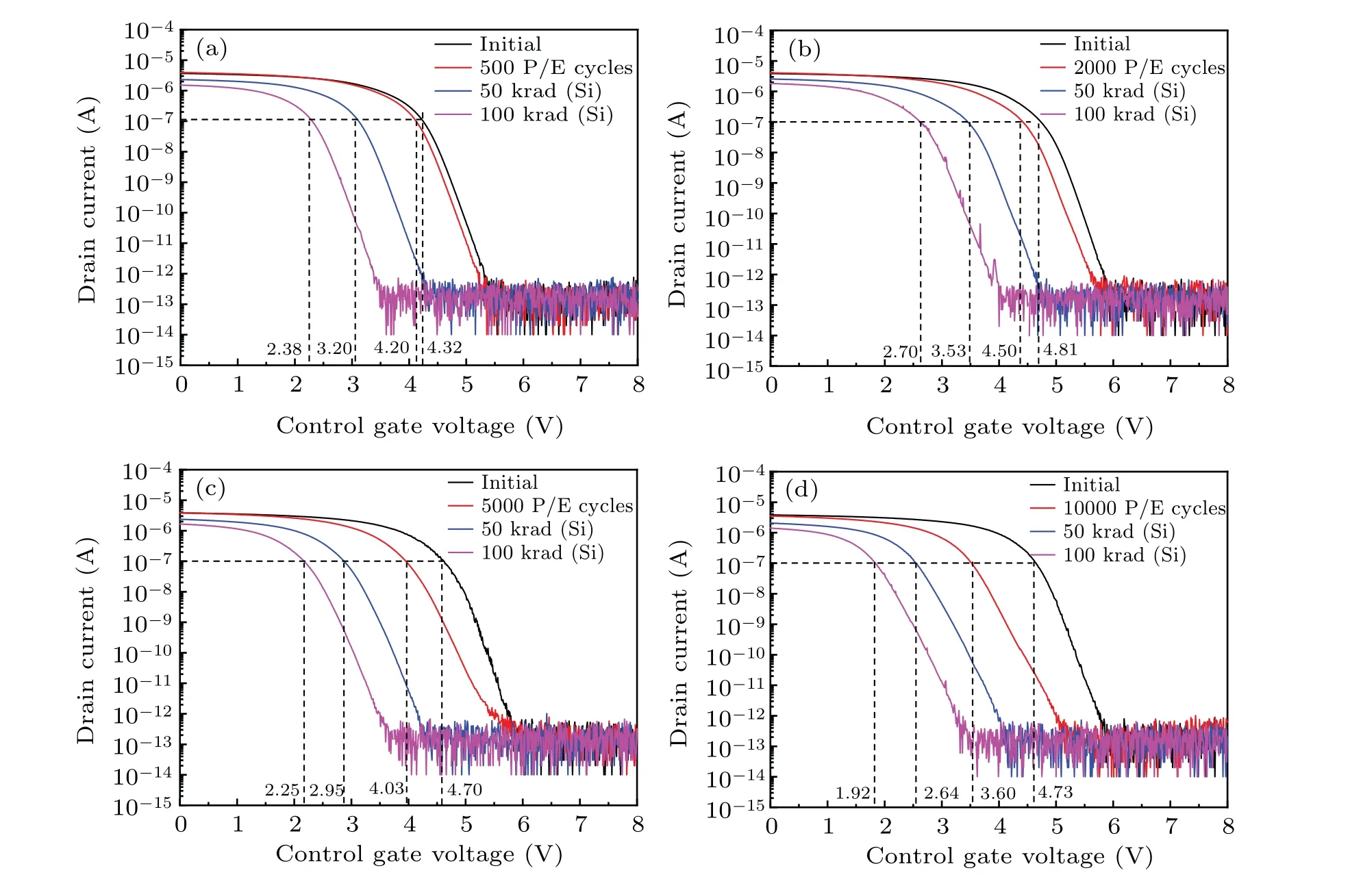
Fig.4. TID characteristics of flash cell with prior P/E cycling numbers(a)500,(b)2000,(c)5000,and(d)10000.
In group 1 the devices is under a prior 2000-P/E cycling stress, the tunnel oxide is subjected to high electrical filed stress, generating oxide traps (mainly electron traps). While the TID also causes the hole to be trapped in the tunnel oxide,there is a possibility that these trapped electrons and trapped holes may be recombined in a very short time as illustrated in process 4 in Fig.3,reducing the electron loss through ΔQtandQiin Eq.(2),resulting in reduced threshold voltage shift compared with the scenario for the devices in group 2.
Also, the influence of prior P/E cycling numbers on the radiation induced threshold voltage shift is investigated, and the results are shown in Fig. 4. After the radiation with the total dose of 100 krad(Si),the threshold voltage shift for flash cells with prior 500-and 2000-P/E cycling stresses exhibits a total threshold voltage shift of about 2 V, while the values of 2.5 V and 2.8 V are in the 5000- and 10000-P/E cycled devices, respectively. The result, in the one hand, proves that the P/E cycling stress before TID can mitigate the radiation induced threshold voltage shift,and,in the other hand,reveals that too many cycling numbers also set up large threshold voltage shift,which is a result of the combined effects of cycling stress and TID.
Furthermore, the combined effects of TID and cycling stress are also studied in the erased state, and the results are described in Fig. 5. Like the programmed state for each of the devices of group 1,the threshold voltage and transconductance before P/E cycling stress are similar to those after the P/E cycling stress, while the transconductance peak value after radiation for each of the devices of group 3 drops much more than that in group 4 devices(see Fig.5(d)),which once again proves that the cycled flash cells are more likely to develop interface state after radiation. By comparison,the major difference between the programmed state and erased state after TID lies in the fact that the latter’s threshold voltage shifts slightly toward the positive direction,which is caused mainly by hole emission in the surrounding oxide. It is also observed that the conductance degradation in group 1(the programmed state)is more severe than in group 3(erased state),illustrating the radiation induced interface trap generation in programmed state is higher than in the erased state.

Fig.5. Electrical characteristics of erased flash cell before and after TID,showing[(a)–(c)]transfer curve,and(d)transconductance curve.
4. Conclusions
In this paper, the combined effects of cycling endurance and radiation on floating gate memory cell are investigated in detail, the results reveal that appropriate P/E cycling number before radiation can mitigate the TID induced threshold voltage shift,which is ascribed to the electron–hole recombination in the surrounding oxides. However, the cycling stress may lead to more severe conductance degradation after radiation,and this is more evident in the programmed state than in the erased state. Thus, the combined effect of cycling stress and TID is a tradeoff between interface state and threshold voltage shift. The result will be useful in understanding the issues involved in cycling endurance and radiation effects as well as in designing radiation hardened floating gate memory cells.
Acknowledgements
Project supported financially by the National Natural Science Foundation of China(Grant No.62174150)and the Natural Science Foundation of Jiangsu Province, China (Grant No.BK20211040).
杂志排行

Chinese Physics B的其它文章
- A nonlocal Boussinesq equation: Multiple-soliton solutions and symmetry analysis
- Correlation and trust mechanism-based rumor propagation model in complex social networks
- Gauss quadrature based finite temperature Lanczos method
- Experimental realization of quantum controlled teleportation of arbitrary two-qubit state via a five-qubit entangled state
- Self-error-rejecting multipartite entanglement purification for electron systems assisted by quantum-dot spins in optical microcavities
- Pseudospin symmetric solutions of the Dirac equation with the modified Rosen–Morse potential using Nikiforov–Uvarov method and supersymmetric quantum mechanics approach