Distribution of donor states on the surface of AlGaN/GaN heterostructures∗
2021-12-22YueBoLiu柳月波HongHuiLiu刘红辉JunYuShen沈俊宇WanQingYao姚婉青FengGeWang王风格YuanRen任远MinJieZhang张敏杰ZhiShengWu吴志盛YangLiu刘扬andBaiJunZhang张佰君
Yue-Bo Liu(柳月波) Hong-Hui Liu(刘红辉) Jun-Yu Shen(沈俊宇) Wan-Qing Yao(姚婉青)Feng-Ge Wang(王风格) Yuan Ren(任远) Min-Jie Zhang(张敏杰) Zhi-Sheng Wu(吴志盛)Yang Liu(刘扬) and Bai-Jun Zhang(张佰君)
1School of Electronics and Information Technology,Sun Yat-sen University,Guangzhou 510006,China
2State Key Laboratory of Optoelectronic Materials and Technologies,Sun Yat-sen University,Guangzhou 510275,China
Keywords: AlGaN/GaN,surface states,exponent distribution
1. Introduction
AlGaN/GaN heterostructure devices have been widely used in high-power, high-frequency electronic devices, because of their wide band gap and high electron mobility.[1–5]The unique electrical properties of the AlGaN/GaN heterostructures benefit from the high density and high mobility two-dimensional electron gas(2DEG),which is formed by the spontaneous and piezoelectric polarization charges at the heterointerface.[6]The donor states on the AlGaN/GaN surface have been widely considered as the source of the electrons in the 2DEG.[7–11]Specifically,Smorchkovaet al.[7]found the 2DEG appeared in Al0.27Ga0.73N/GaN heterostructure when the thickness of the AlGaN barrier was more than 3 nm. The critical thickness of the AlGaN barrier, that is, the minimum thickness allowed the existence of 2DEG,was determined by the energy level position of the donor states on the AlGaN surface. Ibbetsonet al.[8]found the surface donor states were the actual source of the electrons in the 2DEG and the energy level position of the donor states was fixed, which was 1.65 eV below the conduction-band minimum(CBmin)on the Al0.34Ga0.66N/GaN heterostructure surface. Similarly,the valence band maximum can be expressed as VBmax.On the other hand, Koleyet al.[9]found the position of donor states was not fixed and the bare surface barrier height (BSBH) varied according to the AlGaN barrier thickness and the doping concentration. The surface state density can be estimated based on the value of BSBH. Higashiwakiet al.[10]found the surface barrier height monotonically increased with the AlGaN barrier thickness and the surface donor states distributed over a range of energies.Gordonet al.[11]found the highest occupied surface states were about 1 eV below the CBminon surfaces.These models,which consider the electrons in the 2DEG coming from the surface donor states,have been widely used in the analysis of GaN based multiple-channel devices.[12–14]However, the precise features of donor states distribution on Al-GaN/GaN surfaces are still unclear. In previous reports, the density of surface donor states is constant over the range of energy levels.[9,11]
In this work, a common AlGaN/GaN heterostructure and a triple-channel AlGaN/GaN heterostructure are used for Schottky barrier diodes (SBDs), which can provide the carrier concentration profiles of the two materials byC–Vprofiling technique.[15]On the other hand, the carrier concentration profiles can be confirmed by calculation through material structures.[11,16–18]The features of surface donor states distribution are directly related to the carrier concentration profiles in calculation. In our experiments, it is found that the uniform distribution model of surface donor states is not right and the exponential distribution model possibly matches the actual distribution better, especially for the multiple-channel AlGaN/GaN heterostructures.
2. Experiment and analysis
The epitaxy structures of the common AlGaN/GaN heterostructure and the triple-channel AlGaN/GaN heterostructure are illustrated in Fig. 1(a), and the optical microscope photograph of the SBDs are shown in Fig.1(b).
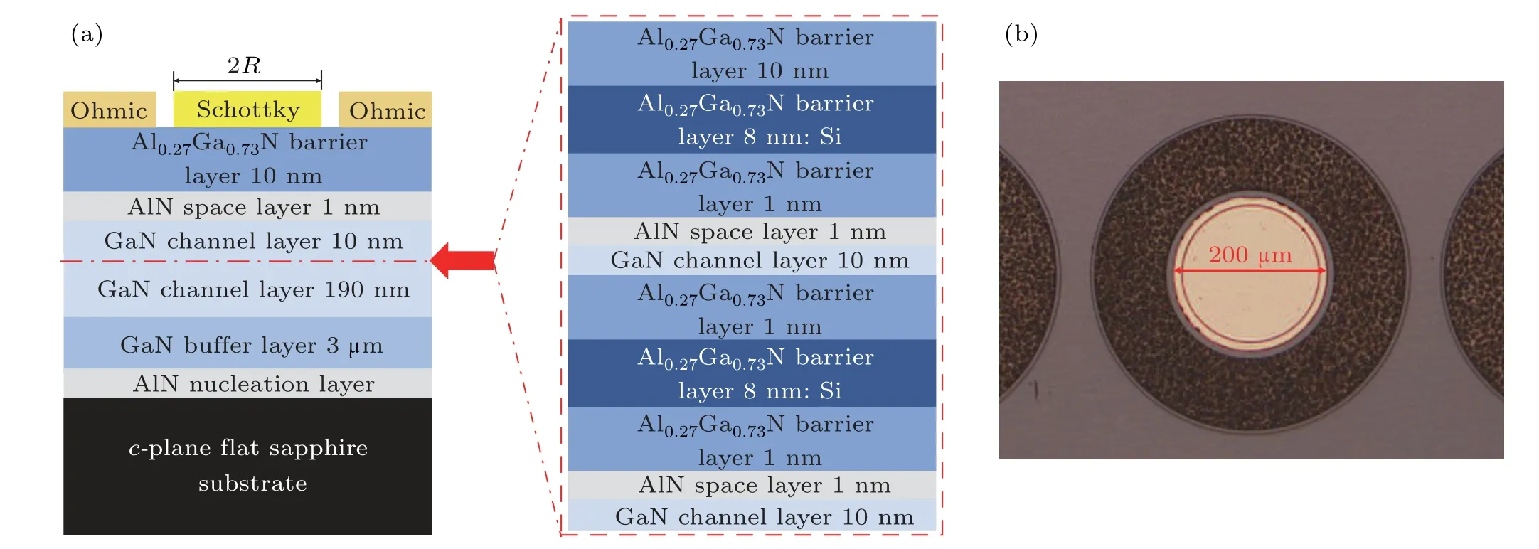
Fig.1. (a)The epitaxy structures of the common AlGaN/GaN heterostructure and the triple-channel AlGaN/GaN heterostructure. (b)The optical microscope photograph of the SBDs and the diameter of the Schottky contact is 200µm.
Samples are grown by metal-organic chemical vapor deposition (MOCVD) system onc-plane sapphire substrates.In epitaxial growth,the common AlGaN/GaN heterostructure starts with an about 20-nm AlN nucleation layer followed by 3-µm unintentionally doped (UID) GaN buffer layer. The channel structure is on the UID GaN buffer layer, consisted of 200-nm UID GaN channel layer, 1-nm UID AlN spacer and 10-nm UID Al0.27Ga0.73N barrier layer from the bottom up. The epitaxy structure of the common AlGaN/GaN heterostructure has been shown in the left half of Fig.1(a). The triple-channel AlGaN/GaN heterostructure is obtained by inserting two additional channel structures into the common AlGaN/GaN heterostructure. Each of the additional channel structures consists of 10-nm UID GaN channel layer,1-nm UID AlN spacer, 1-nm UID AlGaN layer, 8-nm Sidoped Al0.27Ga0.73N layer whose doping concentration is 2×1018cm−3and 1-nm UID Al0.27Ga0.73N layer from the bottom up. The two additional channel structures are shown in the right half of Fig.1(a). The insertion position is 10 nm below the AlN spacer/GaN buffer interface of the common Al-GaN/GaN heterostructure.
The two SBDs are fabricated as the same as the following process. The mesas are fabricated by inductively coupled plasma reactive ion etching (ICP-RIE), and the etching depth of mesas are 200 nm. Then, ohmic contacts consisting of Ti/Al/Ni/Au(20/80/20/60 nm)are formed by rapid thermal annealing (RTA) at 850◦C for 30 s in nitrogen condition. In the final step, the Schottky contacts are formed by depositing Ni/Au(20/60 nm). The radius of the Schottky contacts is 100µm,which has been shown in Fig.1(b).
The capacitance–voltage (C–V) curves of the two SBDs are measured at room temperature and the frequency of the alternating voltage(AC)signal is 100 kHz. The carrier concentration profiles can be acquired by calculation as follows:[15]
whereDis the depletion depth,N(D)is the carrier concentration,Sis the Schottky contact area,εis the vacuum dielectric constant,εsis the relative dielectric constant,andqis the electron charge.
TheC–Vcurves of the common AlGaN/GaN heterostructure and the triple-channel AlGaN/GaN heterostructure are shown in Fig. 2(a). The carrier concentration profiles over depths of the common and triple-channel AlGaN/GaN heterostructures are shown in Fig. 2(b). The peak value of the carrier concentration in the common AlGaN/GaN heterostructure is 5.65×1019cm−3. There are three peaks of the carrier concentration in the triple-channel AlGaN/GaN heterostructure,the peak values are 5.86×1019cm−3,1.34×1018cm−3and 4.21×1019cm−3from the surface down, respectively.It means there are three 2DEGs in the triple-channel Al-GaN/GaN heterostructure.
On the other hand, the distribution of carrier concentration can be confirmed by calculation through material structures. The AlGaN/GaN heterostructures possess polarized wurtzite structures,having dipoles in the[0001]direction. In the absence of external fields, the total polarization consists of spontaneous and piezoelectric polarization, which can be calculated as follows:[16,17]

whereaanda′are the lattice constants of the the upper and lower parts of the heterostructures respectively.crelaxis the relaxation coefficient.e31ande33are the piezoelectric coefficients, andC13andC33are the elastic constants.ns2Dis the concentration of 2DEG.∆PSPequals to the spontaneous polarization of the lower part of the heterostructure minus the spontaneous polarization of the upper part of the heterostructure.εis the permittivity of the materials.
The charge distributionρcan be calculated by the selfconsistent Poisson equation as follows:[18]
whereεijis the second-ranked permittivity tensor,e33is a piezoelectric coefficient,C33is an elastic constant,ϕis the electrostatic potential,andPtotalis the total polarization.
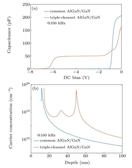
Fig.2. (a)The C–V curves of the common AlGaN/GaN heterostructure and the triple-channel AlGaN/GaN heterostructure. (b)The carrier concentration profiles over depths of the two AlGaN/GaN heterostructures.
Equations (3) and (4) are used to calculate the carrier concentration distribution of the common AlGaN/GaN heterostructure with a uniform distribution model of the surface donor states. In our models, the highest surface donor states are 1 eV below the CBminon surface based on the previous literature,it means the critical surface barrier height is 1 eV.[11]So,the uniform distribution model of the surface donor states of the common AlGaN/GaN heterostructure can be expressed as follows:[11]

whereEis the forbidden bandwidth.Φcis the critical surface barrier height, and its value is 1 eV.nis the constant density of the surface donor states, whose unit is cm−2·eV−1. CBminis the conduction-band minimum on surface.
The calculation results indicate the calculated peak value of the carrier concentration is 5.65×1019cm−3in the common AlGaN/GaN heterostructure when thenis 2.23×1013cm−2·eV−1. The band structure and the distribution of carrier concentration of the common and triple-channel Al-GaN/GaN heterostructures are shown in Fig.3.

Fig.3. The band structure and the distribution of carrier concentration in the common AlGaN/GaN heterostructure(a)and the triple-channel AlGaN/GaN heterostructure(b)with n=2.23×1013 cm−2·eV−1.
As shown in Fig.3(b),in the uniform distribution model,there are only two 2DEGs in the triple-channel AlGaN/GaN heterostructure whennis 2.23×1013cm−2·eV−1. The results show that the surface donor states of the triple-channel AlGaN/GaN heterostructure do not obey the uniform distribution because it cannot provide enough electrons to form three separate 2DEGs.
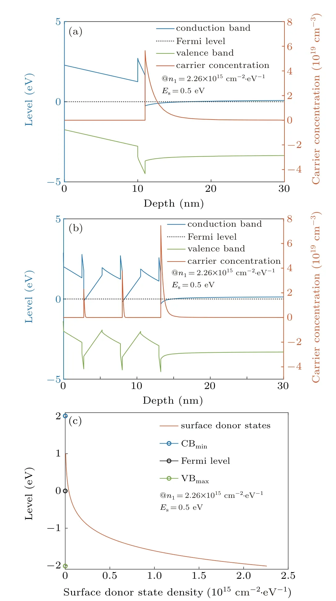
Fig.4. The band structure and the distribution of carrier concentration in the common AlGaN/GaN heterostructure(a)and the triple-channel AlGaN/GaN heterostructure (b) with n1 =2.26×1015 cm−2·eV−1 and Es =0.5 eV. (c)The distribution of the surface donor states. The blue,black and green circles resperent the CBmin,Fermi level and VBmax on surface,respectively.
According to the previous experimental and calculating results, we guess that the level of the surface donor states is closer to the valence band on surface, and the density of the surface donor states is higher. Hence,the exponential distribution model possibly matches the actual distribution of the surface donor states better. The exponential distribution model of the surface donor states in AlGaN/GaN heterostructures can be expressed as follows:

wheren1is the maximum of the surface donor state density in exponential distribution model, whose unit is cm−2·eV−1.CBminis the conduction-band minimum on surface.The range of the exponential distribution is determined byEs. WhenEs=0.5, the highest occupied surface states are 1 eV below the CBminon surfaces according to Eq. (6). The distribution has been shown in Fig.4(c).
In this model, calculations show that the peak value of the carrier concentration is 5.65×1019cm−3in the common AlGaN/GaN heterostructure whenn1equals to 2.26×1015cm−2·eV−1. The band structure and the distribution of carrier concentration of the common and triple-channel Al-GaN/GaN heterostructures have been shown in Figs.4(a)and 4(b). The distribution of the surface donor states is shown in Fig.4(c). The location of 0 eV in Fig.4(c)means the valenceband maximum on surface.
As shown in Fig. 4(b), there are three separate 2DEGs in the triple-channel AlGaN/GaN heterostructure whenn1=2.26×1015cm−2·eV−1andEs= 0.5 eV. The calculation results show the exponential distribution model possibly matches the actual distribution of the surface donor states better,because it allows the 2DEG to form in each channel structure of the triple-channel AlGaN/GaN heterostructure during calculation. The peak values of the carrier concentration are different from the actual peak values,which indicates that the exponential distribution model is still not the actual distribution model of the surface donor states. But the exponential distribution model matches the actual distribution better compared with the uniform distribution model.
3. Conclusion
In this work, we try to verify the uniform distribution model of the surface donor states in AlGaN/GaN heterostructures by experiments and calculations,which has been widely used in the theoretical calculation. A common AlGaN/GaN heterostructure and a triple-channel AlGaN/GaN heterostructure SBDs have been fabricated to verify the models about the distribution of surface donor states. The carrier concentration profiles of the two SBDs are obtained byC–Vprofiling technique. On the other hand, the carrier concentration profiles can be confirmed by calculation through the epitaxy structures of the AlGaN/GaN heterostructures. The features of surface donor states distribution are directly related to the carrier concentration profiles in calculation,so the models about the distribution of surface donor states can be verified by calculating.In the calculation,the highest occupied surface states are 1 eV below the CBminon surfaces. The results show the uniform distribution model is not right,because the surface donor states in this model cannot provide enough electrons to form three separate 2DEGs in the triple-channel AlGaN/GaN heterostructure. Compared to the uniform distribution model, the exponential distribution model possibly matches the actual distribution of the surface donor states better,because it allows the 2DEG to form in each channel structure of the triple-channel AlGaN/GaN heterostructure during calculation. Although the exponential distribution model is still different from the actual distribution model of the surface donor states,we think it would be helpful in the research field.
Acknowledgement
The authors are grateful to Professor Xin-Qiang Wang at Peking University for the support of the common Al-GaN/GaN heterostructure and the triple-channel AlGaN/GaN heterostructure samples.
杂志排行

Chinese Physics B的其它文章
- Transient transition behaviors of fractional-order simplest chaotic circuit with bi-stable locally-active memristor and its ARM-based implementation
- Modeling and dynamics of double Hindmarsh–Rose neuron with memristor-based magnetic coupling and time delay∗
- Cascade discrete memristive maps for enhancing chaos∗
- A review on the design of ternary logic circuits∗
- Extended phase diagram of La1−xCaxMnO3 by interfacial engineering∗
- A double quantum dot defined by top gates in a single crystalline InSb nanosheet∗