Comparison of resonant tunneling diodes grown on freestanding GaN substrates and sapphire substrates by plasma-assisted molecular-beam epitaxy∗
2021-12-22XiangPengZhou周祥鹏HaiBingQiu邱海兵WenXianYang杨文献ShuLongLu陆书龙XueZhang张雪ShanJin金山XueFeiLi李雪飞LiFengBian边历峰andHuaQin秦华
Xiang-Peng Zhou(周祥鹏) Hai-Bing Qiu(邱海兵) Wen-Xian Yang(杨文献) Shu-Long Lu(陆书龙)Xue Zhang(张雪) Shan Jin(金山) Xue-Fei Li(李雪飞) Li-Feng Bian(边历峰) and Hua Qin(秦华)
1School of Microelectronics,University of Science and Technology of China,Hefei 230026,China
2School of Nano-Tech and Nano-Bionics,University of Science and Technology of China,Hefei 230026,China
3Key Laboratory of Nanodevices and Applications,Suzhou Institute of Nano-Tech and Nano-Bionics,Chinese Academy of Sciences,Suzhou 215123,China
Keywords: resonant tunneling diodes,negative differential resistance,molecular beam epitaxy,III-nitrides
1. Introduction
Terahertz(THz)radiation technology has potential applications in many fields such as ultra-broadband wireless communication and security imaging.[1–3]Miniature and solidstate THz sources operated at room temperature are the key factor. Due to high fundamental oscillation frequency and high power,resonant tunneling diodes(RTDs)have been considered as one of the most promising candidates for roomtemperature operating THz oscillators. Kanayaet al.realized an oscillator with frequency of 1.42 THz and output power∼1µW using AlAs/InGaAs/AlAs double-barrier RTDs grown on InP substrates.[4]However,the low output power of less than 1 mW limits the practical applications of InP-based RTD terahertz sources. III-nitride semiconductor materials are suitable for high frequency and power devices because of their excellent properties such as wide bandgap energy,high breakdown fields, high peak electron velocity, high saturated electron velocity,and strong thermal stability.[5,6]Therefore,GaNbased RTDs have attracted more attention in the research field of terahertz sources.[7–17]Many research groups have achieved stable reproducible negative differential resistance(NDR)utilizing RTDs at room temperature.[18–21]Encomenderoet al.reported GaN-based RTDs grown on freestanding GaN (FSGaN) substrates by plasma-assisted molecular beam epitaxy(PA-MBE)with the peak current density(Jp)of 220 kA/cm2,the fundamental frequency of∼0.94 GHz,and output power of∼3.0µW.[22]Later,theJphas been significantly improved and recently reached 1 MA/cm2.[23]In 2019, highly repeatable room temperature NDR was firstly achieved in AlN/GaN RTDs grown on sapphire (Al2O3) substrates by PA-MBE,and theJpwas 164 kA/cm2.[24]Moreover, researchers also studied the repeatable asymmetric resonant tunneling in Al-GaN/GaN double barrier structures grown on sapphire.[25]Based on this series of research results, researchers also proposed the AlN/GaN digital alloy double barrier structure to achieve room temperature NDR.[26]Progress of RTD-related fields have been greatly promoted. Then,Growdenet al.also observed repeatable room temperature NDR for GaN-based RTDs grown on sapphire substrates and obtained the peak current density of 930 kA/cm2.[27]Recently, Choet al.reported the experiment of N-polar RTDs grown on a singlecrystal N-polar GaN bulk substrate to achieve room temperature NDR.[28]In addition,in the past few months,Zhanget al.reported a highly repeatable room temperature NDR in a large area AlN/GaN double barrier RTDs.[29]Nevertheless,current results on RTDs mainly focus on the epitaxial wafers grown on FS-GaN substrates. The main reason is that GaN layers are mismatched with a sapphire substrate. A larger lattice mismatch and a thermal mismatch will bring higher defect densities to the device.More defects will greatly affect the transport of electrons in the vertical direction, resulting in poor device performance, and even the NDR cannot be achieved at room temperature in most cases.[30]However,there are few systematic studies on the effect of two types of substrates on the structure and performance of RTDs and mechanism analysis.
In this work, GaN-based RTDs were grown on FS-GaN substrates and sapphire substrates separately. We obtain the NDR only grown on FS-GaN substrates with a maximum peak current density of 700 kA/cm2and peak-to-valley current ratio(PVCR)of 1.01 for forward bias. The micromorphology and crystal quality of these epitaxial wafers grown on two types of substrates are studied systematically by a variety of characterizations. It found that the main differences for two types of epitaxial wafers are surface morphology and quality of heterogeneous interfaces.
2. Experiment
A schematic of the layers thicknesses and doping of the optimized RTDs structures studied in this paper is given in Fig.1(a). Two 130-nm-thick heavily doped n-type GaN contacts were employed to inject electrons across the doublebarrier structure that consists of 4-nm-thick unintentionally doped(UID)GaN spacers next to each contact,two symmetric 1.5-nm AlN tunneling barriers,and a 2-nm GaN quantum well.The AlN/GaN double barrier structure was grown on FS-GaN substrates and a 4-µm-thick GaN template on sapphire substrates separately by PA-MBE.Silicon(Si)was used as n-type doping sources. The substrates were firstly solvent cleaned and loaded into the load lock chamber. Before growing,twostep out-gassing bakes need to be performed for thermal cleaning of the substrate’s surface at 250◦C for 2 h and followed by 760◦C for 0.5 h. Epitaxial layers of AlN/GaN RTDs were grown sequentially according to the simulated epitaxial structure. The growth temperature of the active region was maintained at 810◦C. The nitrogen flow rate and the rf-plasma power were 1.5 sccm and 350 W, respectively. The growth temperature was monitored by using BandiT, and the surface conditions were monitoredin situusing reflection high energy electron diffraction (RHEED). The growth rates of AlN and GaN layers estimated from their thicknesses were 135 nm/h and 145 nm/h,respectively. RTDs grown on the sapphire substrates and FS-GaN substrates were marked as samples A and B,respectively.

Fig.1. (a)The epitaxial structure schematic of GaN-based RTDs grown on two types of substrates,(b)optical microphotograph,and(c)SEM picture of RTDs.
The RTDs were fabricated using conventional semiconductor device processing methods.The devices went through a standard cleaning process using H2SO4and H2O2with a ratio of 7:3 for moving metal droplets from the surface. After that,the surface was covered with a photoresist of AZ6130. Immediately following the resist treatment, optical lithography was used to forming etching patterns. The mesa was defined using ICP that has a high power to ensure vertical sidewalls through the active region. The second photomask was used to define the top contact. Electron beam(e-beam)evaporation was used to deposit a Ti/Al/Ni/Au top contact. Afterward,device isolation pads were defined with the third photomask. A passivation layer of SiO2was deposited by plasma-enhanced chemical vapor deposition to ensure the insulation between pads. The optical microphotograph and scanning electron microscopy (SEM) of RTDs were shown in Figs. 1(b) and 1(c),respectively.
Electrical characterization of the RTDs was carried out with a Keysight 4200 semiconductor parameter analyzer.Atomic force microscopy (AFM), cathode-luminescence(CL), high-resolution x-ray diffraction (HRXRD), and scanning transmission electron microscopy (STEM) were used to characterize the micromorphology and crystal quality of RTD epitaxial wafers.
3. Results and discussion
3.1. The I–V measurement results of RTDs grown on different substrates
Figures 2(a) and 2(b) displaces theI–Vcharacteristic curves of RTDs grown on different substrates. RTDs grown on FS-GaN substrates exhibit clear NDR at room temperature for forward bias as described in Fig.2(b)with theJpof 175–700 kA/cm2and the PVCR of 1.01–1.21,while NDR is not observed in the RTDs grown on sapphire substrates as shown in Fig.2(a).The RTDs mesa diameter is 4µm in Fig.2(b).Moreover,two resonant peaks are observed in some RTDs grown on FS-GaN substrates at room temperature as displaced in the inset of Fig.2(b). Regrettably,the room-temperature NDR characteristic could be observed in the first scan of these samples,but it disappears in the subsequent scans as shown in the blue curve in Fig.2(b). Figure 2(c)shows the room-temperatureI–Vcurves of RTDs with mesa diameters of 1/2/4/8µm. As can be seen from Fig.2(c),NDR occurs for RTDs of different sizes under forward bias,although only once. This phenomenon is consistent with the RTDs observed earlier and may be due to the current instability caused by the trap effect.[30]In addition, the simulation results of the device are compared with the experimental results. Here, 1, 2, and 3 marked in the figure indicate the resonant tunneling locations. Figures 2(b)and 2(c)are the experimental measurements,Fig.2(d)is the simulation result of the device structure. The voltage ranges at position 1 are 4.27–4.5 V,the voltage ranges at position 2 are 4.86–5.43 V, and the voltage ranges at position 3 are 5.7 V in Figs. 2(b) and 2(c). By comparing (b), (c), and (d), it can be seen that although the experimental value and the design value are not perfectly consistent,they are basically within the corresponding ranges.

Fig. 2. The I–V characteristic of RTDs grown on (a) sapphire substrates and (b) FS-GaN substrates. The inset shows two resonant peaks in some devices. (c)The I–V relationships for different device sizes. (d)Simulation results of the device.
We speculate that the main cause of problems including no NDR in the RTDs grown on sapphire substrates and unreproducible NDR in the RTDs grown on FS-GaN substrates is attributed to microstructure and crystal quality. Therefore,we studied it systematically by analyzing and comparing the microscopic differences between the epitaxial wafers of RTDs grown on the two types of substrates.
3.2. Comparison of epitaxial growth characterization of devices
AFM images of samples A (sapphire substrates) and B(FS-GaN substrates)were illustrated in Figs.3(a)and 3(b),respectively. The rms roughness of the surface with a scanning area of 5µm×5µm was 0.49 nm and 0.28 nm,respectively. It can be seen that sample A has a hill-rock morphology, while sample B exhibits a regular step-flow feature and atomically smooth surface. This result may be related to lower thermal conductivity and larger dislocation densities of the sapphire substrates. On the one hand,at the same growth temperature,gallium (Ga) atoms have lower mobility at the front surface on sapphire substrates which affect the atoms distribution and step coverage of thin films; on the other hand, GaN epitaxial wafers grown on the sapphire substrates will naturally result in higher dislocation densities due to the larger lattice mismatch.The effects of silicon doping and high dislocation densities for sapphire substrates even lead to the generation of defect pits as shown in Fig. 3(a).[31]Consequently, a poor surface was obtained for RTD wafer grown on sapphire substrates.
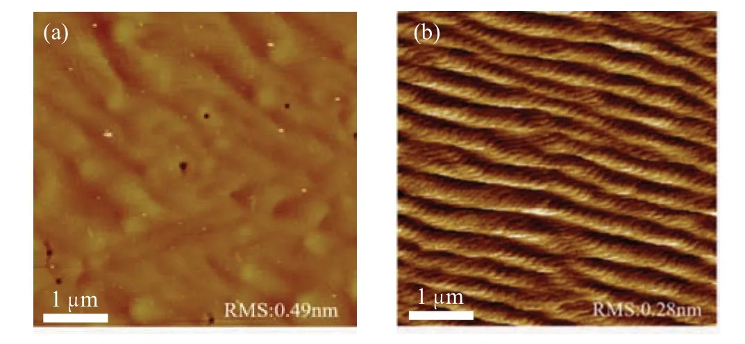
Fig.3.AFM images of RTD wafers grown on(a)sapphire substrate and(b)FS-GaN substrate.
Dislocation is one of the important factors for RTD wafer quality, and its density will affect greatly on NDR characteristic and peak current densities of the device. As shown in Fig. 4, the x-ray diffraction rocking curves of GaN epitaxial layers grown on sapphire substrates and FS-GaN substrates were measured to estimate total dislocation densities.[32,33]
The full widths at half maximum (FWHMs) of x-ray rocking curves along the (002) plane for the two samples are 248 arcsec and 135 arcsec,and those are 285 arcsec and 91 arcsec along the(102)plane, respectively. The densities of total dislocations were calculated using the formulae[34]
where TDDt, DDs, and DDtare the total dislocation density,screw dislocation density, and edge dislocation density, respectively;βrepresents the FWHMs that are measured by HRXRD rocking curves, andbis the Burgers vector length to be 0.5185 nm and 0.3189 nm, respectively.[35]According to formulae (1)–(3), the calculated GaN layers edge and screw densities values are listed in Table 1. The total dislocation densities of the GaN epitaxial layer grown on sapphire substrates and FS-GaN substrates are 5.5×108cm−2and 8.1×107cm−2, respectively. These results are higher than the dislocation density threshold of 3.96×107cm−2reported in the literature for observable repeated NDR.[29]As for GaN-based RTDs,these defects can be acted as carrier traps to induce current leakage and even mask the resonant tunneling transport.[36,37]Thus, the trap effect may be the main direct reason for no NDR in sample A and irreproducible NDR in sample B at room temperature.Therefore,the dislocation densities of GaN-based RTD wafers need to be decreased further to achieve stable NDR.
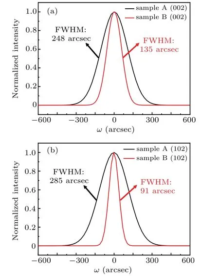
Fig. 4. X-ray diffraction rocking curves along (a) the (002) plane and(b)the(102)plane of RTD wafers grown on two types of substrates.
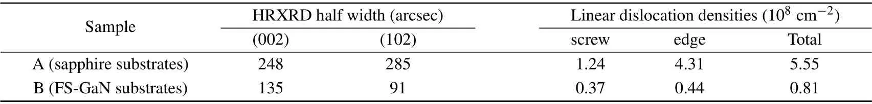
Table 1. Dislocation densities of GaN epitaxial layers grown on two types of substrates.
Furthermore, we employ CL to realize the macroscopic characteristics of threading dislocations,and the approximate dislocation densities can be estimated based on the surface luminescence.[38]Figure 5 presents the CL images of samples A and B,where the black dots in the figure indicate threading dislocations. It can be found that the dislocation densities of sample A are significantly higher than those of sample B.The calculated dislocation densities of RTDs grown on sapphire substrates and FS-GaN substrates are 108cm−2and 106cm−2,respectively.
High-quality ultrathin AlN/GaN double-barrier structure is the key to achieving NDR in GaN-based RTD. Figure 6 presents STEM images of the AlN/GaN double-barrier structure in two RTD samples. Firstly, clear and abrupt AlN/GaN hetero-interfaces are observed in sample B grown on FS-GaN substrates, whereas hetero-interfaces are indistinct for sample A grown on sapphire substrates. Secondly, the deviation between the measured thickness and the design thickness of AlN barrier layers is within 0.2 nm, but the thickness deviations of GaN well for the two RTD samples reach 28% and 1%, respectively. Consistent with the AFM measurement results, FS-GaN substrates can enhance nucleation and crystallization of GaN and AlN material because of atomic mobility and incorporation effectively and few defects during the epitaxial growth. Consequently, the thicknesses of epitaxial layers are controlled atomically and abrupt hetero-interfaces are achieved in GaN-based RTDs grown on FS-GaN substrates.

Fig. 5. CL images over 25.5 µm×25.5 µm of RTD epitaxial wafers grown on(a)sapphire substrate and(b)FS-GaN substrate.
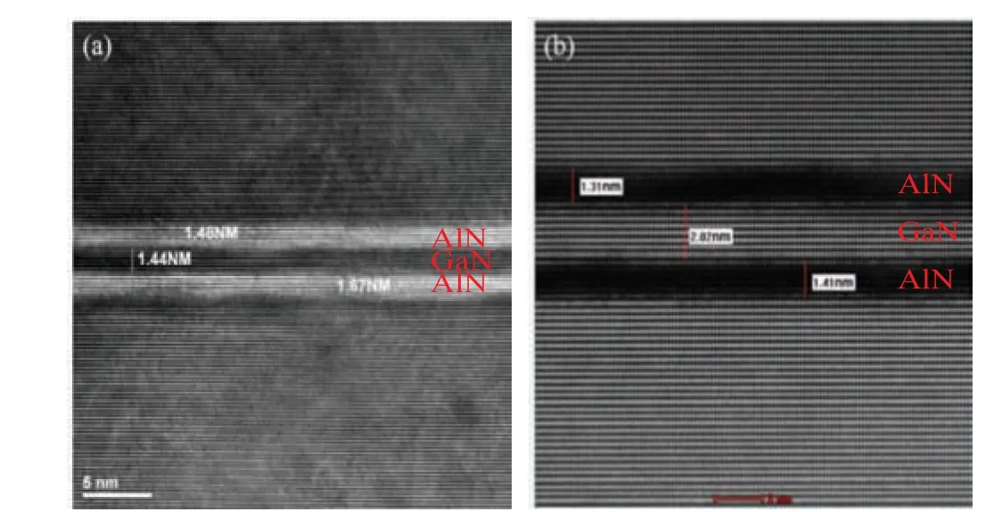
Fig. 6. STEM images of the AlN/GaN double barrier structure in RTDs grown on(a)sapphire substrates and(b)FS-GaN substrates,respectively.
4. Conclusion
In summary, AlN/GaN RTDs grown on sapphire substrates and FS-GaN substrates by PA-MBE have been prepared separately. Two resonant peaks were observed for RTDs grown on FS-GaN substrates, and the peak current densities range from 175 kA·cm−2to 700 kA·cm−2under forward bias at room temperature. Furthermore, no NDR was observed in RTDs grown on the sapphire substrates. A series of comparative experimental results show that RTD epitaxial wafers grown on FS-GaN substrates have lower dislocation densities,better surface morphology, and sharper heterogeneous interfaces, which are the keys to achieving reproducible NDR at room temperature. Therefore, the growth and mechanism of GaN-based RTDs on two types of substrates by MBE need to be investigated more deeply.
猜你喜欢
杂志排行

Chinese Physics B的其它文章
- Transient transition behaviors of fractional-order simplest chaotic circuit with bi-stable locally-active memristor and its ARM-based implementation
- Modeling and dynamics of double Hindmarsh–Rose neuron with memristor-based magnetic coupling and time delay∗
- Cascade discrete memristive maps for enhancing chaos∗
- A review on the design of ternary logic circuits∗
- Extended phase diagram of La1−xCaxMnO3 by interfacial engineering∗
- A double quantum dot defined by top gates in a single crystalline InSb nanosheet∗