Solar broadband metamaterial perfect absorber based on dielectric resonant structure of Ge cone array and InAs film*
2021-11-23KuangLingGuo郭匡灵HouHongChen陈厚宏XiaoMingHuang黄晓明TianHuiHu胡天惠andHaiYingLiu刘海英
Kuang-Ling Guo(郭匡灵), Hou-Hong Chen(陈厚宏), Xiao-Ming Huang(黄晓明),Tian-Hui Hu(胡天惠), and Hai-Ying Liu(刘海英)
Guangdong Provincial Key Laboratory of Nanophotonic Functional Materials and Devices,School for Information and Optoelectronic Science and Engineering,South China Normal University,Guangzhou 510006,China
Keywords: metamaterial,electromagnetic resonance,perfect absorber,solar broadband absorption
1. Introduction
In recent years, people have paid more and more attention to solar energy because of its excellent renewability and environment-friendly property. In order to efficiently utilize solar energy, the first thing that needs to do is to build a perfect absorption platform, which should have the ability to absorb broadband light. Meanwhile, the metamaterial with the outstanding properties of light absorption[1,2]has been widely studied and applied to many aspects, such as thermal emitting,[3,4]bio-sensing,[5-7]photothermal,[8,9]photoelectric detecting,[10,11]power harvesting devices,[12,13]etc. In 2008,Landyet al. first proposed the metamaterial perfect absorber(MPA)based on the metal-dielectric-metal structure.[14]Nevertheless,the resonance in the metamaterial is always limited in a narrow wavelength range, which results in the narrowband absorption.[15-19]In order to achieve broadband absorption,the most critical problem is how to widen the absorption windows. The most common solution to this problem is to construct special structures, such as cubes, disks,etc. Akselrodet al. used Ag nanocubes to obtain the perfect absorption in visible and near-infrared range.[20]Lianget al. disigned an absorber based on titanium nitride nano-disks,which exhibits near-unity absorption in the whole visible range.[21]However,owing to the high symmetry of the cubes and disks, the generation of many resonance modes is restricted,and perfect absorbers based on these high-symmetry structures can achieve the perfect absorption only in a range from visible to nearinfrared light. Therefore,the introduction of asymmetric parts into the traditional high-symmetric structures may increase resonance modes of the structures, which makes it possible to cover the whole solar absorption spectrum.
Traditional metamaterial perfect absorbers are mostly based on metal surface plasmon resonance. However, inevitable intrinsic loss effects (such as nonradiative ohmic losses)[22]in metal materials cause energy dissipation, and thus affecting the resonance absorption of the system. Compared with the general noble metal, the dielectric with a high refractive index (e.g., Si, Ge, GaAs, InAs,etc.) possess slight inherent loss which enables the broadening of the absorption spectrum. Meanwhile, extraordinary optical Mie resonances[23,24]are observed in dielectric materials with a high refractive index: as a matter of fact, not only the electric dipole resonance but also the magnetic dipole, magnetic quadrupole, and even some high order resonance modes are observed.[25,26]As a preferred material of microelectronics,germanium(Ge),a kind of high refractive index semiconductor material,is widely used in optical detectors[27-30]and optical fiber sensors,[31,32]because of its low energy consumption and good performance in the infrared band. The InAs,a type of III-V type combined semiconductor material, has a significant absorption effect in the near-infrared region,meanwhile, it also has considerable electron mobility, hole mobility, relatively small magnetoresistance effect, and resistance temperature coefficient. Thus, it is used to manufacture fiber laser[33,34]and sensor[35,36]in the near-infrared band.
In this study, a solar broadband metamaterial perfect absorber(SBMPA)is proposed based on the structure of Ge cone array and the InAs dielectric film on the gold (Au) substrate.In a solar spectrum range from 200 nm to 3000 nm, the proposed absorber absorbs more than 98.7%of the solar energy.Meanwhile,in a range from 200 nm to 1430 nm,the absorber presents a perfect absorption window where the absorptivity exceeds 99%. Analyzing the field distribution in near-perfect absorption peaks, different resonance modes are observed in the simulation. The Ge cones have asymmetry around the direction of light propagation, and can realize more resonant modes. Electric dipole resonance,magnetic dipole resonance,electric quadrupole mode,magnetic quadrupole mode,and the high order modes in the Ge cones are the main reason for broadband absorption.The proposed absorber may well be applied to active photoemission,thermion modulation,and photoelectric detection.
2. Metamaterial absorber and methods
The schematic diagram of the proposed absorber and the unit cell are shown in Figs. 1(a) and 1(b) respectively. As shown in Figs.1(a)and 1(b),the absorber consists of Ge cone array and InAs dielectric film on the gold substrate.The height of the Ge cone (H), InAs dielectric film (h1), and gold substrate (h2) are 1500 nm, 900 nm, and 100 nm respectively.The apex angle (θ) of the Ge cone is set to be 19°and the array period(P)is 502 nm.

Fig.1. (a)Perspective views of SBMPA,the upper for Ge, the middle for InAs, the lower for Au; (b)a unit cell, with thickness(h1)of InAs being 900 nm, thickness (h2) of Au film being 100 nm, height (H) of the Ge resonator being 1500 nm,apex angle being 19°,and period(P)being 502 nm.
We calculate and obtain the absorption properties of SBMPA by FDTD solutions. In the simulation, we set periodic boundary conditions in bothxandydirections to reduce the calculating loads,and choose the perfect match layer boundary condition in thezdirection in order to eliminate the influence of the scattering. The simulated light source is thexpolarized plane waves ranging from 200 nm to 3000 nm. The permittivity of Ge refers to the data of CRC[37]while the permittivity values of InAs and Au refer to the data of Palik.[38]The absorption is defined byA=1−R −T, whereRandTdenote reflection and transmission respectively. For the intact absorption,the minimizing of the reflection and the transmission is essential. We choose an appropriate thickness of the gold substrate according to the penetration depth of the electromagnetic wave(δ)[39]which can be express as

whereωis the frequency of light,µis the magnetic permeability of Au,σis the conductivity of Au. The calculation results show that when the thickness of the Au film is no less than 39 nm, the energy transmitting through the Au substrate is negligible. Therefore,we set the thickness of the Au film to be 100 nm,which makes the transmission of the system almost get to zero,namely,T=0.So the absorption can be simplified intoA=1−R.
3. Numerical analysis and discussion
3.1. Performances and principles
Figure 2 shows the reflection and absorption of the SBMPA. The blue solid line represents transmission (T), the solid black line the reflection (R), and the red solid line the absorption (A). The light absorption (A) can be defined asA=1−R −T, where the transmission in this absorber is almost suppressed (T= 0). After calculation, the absorption efficiency exceeds 99% in the wavelength range with strong solar radiation of 200 nm-1430 nm. In other words, the absorption window of the SBMPA covers the whole range of visible and near-infrared light and achieves a near-perfect absorption. According to the above data analysis, the SBMPA has near perfect absorption performance.

Fig.2. Simulation results of proposed metamaterial perfect SBMPA,with black solid line representing reflection (R), blue implementation denoting transmission(T),and the red solid line referring to absorption(A).
We also study the solar absorption characteristics of the SBMPA and evaluate its potential performance in energy collection. In this work,we place the SBMPA under the ideal solar AM 1.5 light source to study the solar energy absorption efficiency. The spectrum ranges from ultraviolet to near infrared(200 nm-3000 nm) light. As shown in Fig. 3, the spectral curves of the SBMPA almost coincide with the spectral curves of standard solar source under solar irradiation. In order to define the absorption response of solar energy,the spectral curve of unabsorbed solar energy is obtained by subtracting the energy absorbed by the SBMPA from the source energy by the AM 1.5. According to the calculation, the SBMPA can absorb more than 98.7%of the solar energy. This shows that the use of active photoelectric effect, thermionic related modulator,and photodetector under solar are all feasible in the future research.

Fig.3. Absorption efficiency of the structure under solar AM 1.5 light source.
Further, in order to clearly understand the absorption response of the SBMPA, we analyze the resonance modes of the structure at near-perfect absorption peaks,and four absorption peaks areλ1=220 nm,λ2=500 nm,λ3=748 nm,andλ4=1388 nm. Figures 4 and 5 illustrate the electric and magnetic field distribution maps of four-unit structures on thexoyplane andxozplane. The sufficient height of Ge cone provides conditions for a variety of different field distribution patterns,and the positions of thexoyplane intercepted are the semiheight plane of Ge cone and the contact surface between the bottom of Ge cone and the top of InAs dielectric film.
Figure 4 respectively shows the electric field distribution ofλ3= 748 nm (Figs. 4(a)-4(c)) andλ4= 1388 nm(Figs.4(d)-4(f)). From top to bottom of each panel are shown thexozplane, thexoyplane at the semi-height of Ge cones and thexoyplane at the contact surface between the bottom of Ge cones and the top of the InAs dielectric film. Electric filed resonance modes are the main factors of perfect absorption at these wavelengths. Figure 4(a) shows the distribution of the electric field in thexozplane atλ3=748 nm. It can be seen that the electric field is localized mainly on the surface of the Ge cones and the electric quadrupole resonance(EQ)is formed on the axis of the cone along the direction of light polarization by observing the electric field distribution diagram in thexoyplane at the half-height of the Ge cones in Fig.4(b).Then,in Fig.4(c),a high-order conducting membrane[40]appears in the system. Thus, the electric quadrupole resonance and high-order conducting membrane are formed at this wavelength stimulated perfect absorption.

Fig.4. Electric field distribution at[(a)-(c)]λ3=748 nm and[(d)-(f)]λ4 =1388 nm. From top to bottom of each panel are shown the xoz plane and the xoy plane at the semi-height of Ge cones, and the xoy plane at the contact surface between the bottom of the Ge cones and the top of the InAs dielectric film.
For a wavelength of 1388 nm as shown in Figs.4(d)-4(f),there is a strong electric field in Ge cones and in the InAs dielectric film as well. Moreover,a strong electric field is localized in the gap at the bottom of the cone. The electric dipole resonance (ED) is formed in Ge cones, indicated through the analysis of the electric field distribution in the direction ofxoyin Fig.4(e). Finally,as shown in Fig.4(f),we can observe that the electric dipole resonance is formed at the bottom of Ge cones. Since the distance between Ge cones is very small in the periodic structures,the gap coupling is formed between the electric dipole resonances, making the electric field localized in the gap.
Figure 5 plots the magnetic field distribution ofλ1=220 nm [(a)-(c)] andλ2=500 nm [(d)-(f)] in thexozplane and thexoyplane. First, as shown in Fig. 5(a), the field distribution image clearly shows that the magnetic field atλ1= 220 nm is not concentrated inside the Ge cone, but mainly on the surface of Ge cones which means that the magnetic reaction mainly originates on the outer surface of the cone rather than inside the cone. In Fig. 5(b), there is an interaction between adjacent Ge cones which is often called coupling. Due to the coupling effect,we can find that a local magnetic field is formed in the center of the four Ge cones.Furthermore, by observing the magnetic field distribution in Fig.5(c),we can find that the magnetic quardrupole resonance(MQ)is formed among four Ge cones,which results in perfect absorption at this wavelength. Finally,as seen in Fig.5(d),the magnetic field also concentrates primarily on the surfaces of Ge cones and the gaps at the bases of Ge cones atλ2=500 nm.According to Fig. 5(e), a magnetic dipole resonance (MD) is formed on the surfaces of Ge cones. Owing to the close arrangement of the cones,the magnetic dipole resonance modes of different cones will be coupled with each other as shown in Fig.5(f),which illustrates the existence of resonance coupling at the bottoms of the Ge cones. Therefore, the main reason for the perfect absorption at this wavelength is the magnetic dipole resonance formed on the surfaces of Ge cones. It can be seen that the main reason for the perfect absorption at these two wavelengths is related to the magnetic field reaction.Generally, the structure achieves different modes of resonance at different heights of the Ge cones,and because of its good coupling of the resonant modes,it can achieve perfect absorption over a large band range.

Fig. 5. Magnetic field distribution at [(a)-(c)] λ1 =220 nm [(a)-(c)]and[(d)-(f)]λ2=500 nm. From top to bottom of each panel are shown the xoz plane,the xoy plane at the semi-height of the Ge cones and the xoy plane at the contact surface between the bottom of the Ge cones and the top of the InAs dielectric film.
3.2. Effects of geometry and material on absorption performance
In order to have a further understanding of the working mechanism of the SBMPA,we study the absorption response under different structural parameters. Figure 6(a) shows the variation of absorption response of the SBMPA with the InAs dielectric film thickness(h1). As the thickness of InAs gradually increases,the absorption spectrum of the SBMPA shows a significant redshift in the simulated range,and the wavelength range that could reach the perfect absorption continues to increase. Moreover,when the thickness is larger than 1000 nm,the SBMPA generates a new absorption peak at a wavelength of 2500 nm.
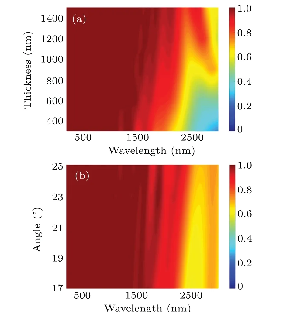
Fig.6.Perfectly adjustable metamaterial absorber obtained by changing structural parameters, showing change in absorption spectrum caused by(a)InAs thickness,and(b)transformation of Ge angle ranging from 17° to 25°.
Figure 6(b)shows the absorption response of the SBMPA when the apex angle (θ) of the Ge cone is changed. We can find that the change of the apex angle has little influence on the absorption performance of the absorber. However,with the increase of the angle, the absorption spectrum of the absorber still shows a small amount of redshift. This indicates that the error range tolerant in device manufacturing is large.
We also consider the effect of the height (H) of cone on the absorption performance. As shown in Fig.7,we compare the difference among absorption intensities at different heights ranging from 1000 nm to 2000 nm. It can be clearly seen that the absorption spectrum widens slightly as the height of the cone increases. WhenHis 1500 nm,the two weak absorption gaps from 1500 nm to 1900 nm and from 2300 nm to 2700 nm disappear. And further increasing the height of the cone has no significant effect on the absorption intensity. Weighing the fabrication process and absorption effect,we finally chose the height of the simulated structure to be 1500 nm.

Fig.7. Absorption renderings of different heights of cones.

Fig. 8. Absorption curves of different materials, with (a) keeping Au and InAs unchanged and replacing Ge material with InAs,InP,TiN,and GaAs;(b)keeping Au and Ge unchanged and replacing InAs dielectric film with InP,Ge,TiN,and GaAs.
Next,we use different materials to replace Ge cones and InAs dielectric film respectively while keeping the structure size unchanged. In Fig. 8 are summarized the absorption responses of metamaterial perfect absorbers for cones and dielectric film under different materials. Figure 8(a) shows the graph of replacing Ge with other semiconductor materials(such as InAs,InP,TiN,and GaAs)while keeping Au and InAs unchanged. The comparison of the data shows that the Ge and InAs have better absorptions in the visible light and nearinfrared region, while TiN has better absorption performance in the near-infrared region. Figure 8(b) shows the absorption behaviors of the InAs dielectric layer replaced by other highindex dielectrics (such as Ge, TiN, and GaAs), with Au and Ge unchanged. As can be seen from this figure,the InAs material has a better absorption effect on the energy absorption of sunlight in a wavelength range from 300 nm to 2200 nm,while TiN material as a whole has a broader absorption window. The above results show that strong absorption can be observed from all the types of materials we have selected.Different materials are used in different fields,indicating that the proposed SBMPA will have a wide range of applications.
Finally, we also study the variation of the absorption spectrum at different polarization angles as shown in Fig. 9.When the polarization angle changes from 0°(electric fieldEparallel to thexaxis) to 90°(electric fieldEparallel to theyaxis), the SBMPA has polarization-independent absorption characteristics. The main reason for the polarizationinsensitive phenomenon is the high-symmetry SBMPA.[41,42]The polarization-independent metamaterial perfect absorber has been widely used in the relevant solar energy absorbing devices.[43,44]

Fig.9. Absorption diagram of polarization angle increasing from 0° (electric field E parallel to x axis)to 90° (electric field E parallel to y axis).
4. Conclusions and perspectives
In this work is proposed and demonstrated an SBMPA based on the structure of Ge cone array and the InAs dielectric film on the gold substrate. In the solar spectrum from 200 nm to 3000 nm,the proposed absorber is able to absorb more than 98.7%of the solar energy,and the proposed absorber presents a perfect absorption window where absorptivity exceeds 99%in a wavelength range from 200 nm to 1430 nm. Mie resonance modes exist in the Ge cones, and high-order modes play important roles in bandwidth absorption.In a short wavelength range,the perfect absorption is mainly due to the magnetic resonances,such as magnetic dipole resonance and magnetic quadrupole resonance. In the long-wavelength range,the perfect absorption is mainly due to the electric resonances and the high-order modes. In addition, the perfect absorption is also achieved by using different materials instead of patterned Ge and InAs layer,which indicates that the SBMPA has good adaptability to a wide range of material. The SBMPA is of significant potential applications in the active photoelectric effect,thermion modulation,and photoelectric detection.
猜你喜欢
杂志排行

Chinese Physics B的其它文章
- Numerical investigation on threading dislocation bending with InAs/GaAs quantum dots*
- Connes distance of 2D harmonic oscillators in quantum phase space*
- Effect of external electric field on the terahertz transmission characteristics of electrolyte solutions*
- Classical-field description of Bose-Einstein condensation of parallel light in a nonlinear optical cavity*
- Dense coding capacity in correlated noisy channels with weak measurement*
- Probability density and oscillating period of magnetopolaron in parabolic quantum dot in the presence of Rashba effect and temperature*