Design and optimization of a nano-antenna hybrid structure for solar energy harvesting application
2021-09-28MohammadJavadRabienejhadMahdiDavoudiDararehandAzardokhtMazaheri
Mohammad Javad Rabienejhad,Mahdi Davoudi-Darareh,and Azardokht Mazaheri
1Optics and Laser Science and Technology Research Center,Malek Ashtar University of Technology,Shahinshahr,Iran
2Faculty of Science,Department of Physics,Malek Ashtar University of Technology,Shahinshahr,Iran
3Department of Physics,University of Isfahan,Iran
Keywords:field electron emission,infrared,metal–insulator–metal(MIM)diode,nano-antenna,photovoltaic effects,rectification,solar energy harvesting
1.Introduction
The sun is the most reachable energy source that performs a continuous stream of power;its benefit has stimulated several methods and technologies to achieve renewable energy.The sun emits electromagnetic radiation(UV,visible spectrum,and near-IR)to the earth along the day.Almost 30%of this energy is reflected from the atmosphere into space,and 19%is absorbed by atmospheric gases.Much of the UV radiation is absorbed and reflected by the ozone layer and atmospheric barrier.So,almost all the energy reaching the earth is more in both the visible and IR regions.The remaining 51%of the emitted energy is absorbed by the earth’s surface.[1]So,the ground heats up and re-emits the energy in the mid-infrared(MIR)range.[2]Most of the earth’s surface is filled by water,and since the specific heat capacity of water is greater than that of the soil,this energy re-emission will continue throughout the night.
Photovoltaic(PV)solar cells have been used for many years to harvest solar energy,but there are several restrictions on their use.[3]One of them is their low efficiency.An individual PV cell has a conversion efficiency of about 29%,and multi-junction cells have a conversion efficiency of almost 46%.[4]Also,these devices have a limitation in solar energy harvesting in night.
The proposed structure in this study transmit and save the re-emitted MIR radiation from the earth.So,the rectenna(nano-antenna plus rectifier),utilizing a nano-antenna coupled to a rectifier to convert the accumulated re-emitted solar energy from the earth into DC power during a daytime and a nigh,is proposed based on the specificity of the light wave.In general,this system consists of a nano-antenna,a rectifying diode(such as a metal–insulator–metal(MIM)diode),and a DC pass filter.[5,6]
The nano-antennas[7]are fabricated from a few hundred nanometers to several micron,which have been recently investigated thanks to the development of the electron beam lithography and the semiconductor fabrication method.They offer potential benefits of tunability in size and performance parameter,and fast time response.[8–10]The solar harvesting efficiency and the low input impedance of the rectennas are investigated in different shapes of nano-antenna,such as bowtie,spiral,log-periodic,flower-shaped dipole,and elliptic dipole nano-antenna.[11–17]
The movement of electrons creates an AC-current in the antenna circuit.Because the purpose of these devices is to supply external load,the AC-current must be rectified by a proper diode.[18,19]The MIM[20–24]and Esaki[25,26]diodes have been used in the rectification mechanism based on tunnel conduction to enhance the switching frequencies in diode performance.The MIM diodes attract more interest as a candidate for high wavelength applications.[27]The MIM is a thinfilm device consisting of a very thick insulator layer placed between the two metallic electrodes.[28,29]This diode employs the electron tunneling process through the insulator to rectify the AC signa.Eventually,the idea of utilizing rectennas to harvest the sunlight and the earth’s re-emitted solar energy to generate power has been proposed.
In the MIM diode,the metal’s work function is higher than the electron affinity of the insulator,which conflicts with the metal/insulation interface.Charge transport within the insulator happens due to the quantum-mechanical tunneling of the electron.[30]The probability of transmission is associated with the possibility of electron tunneling through the classically forbidden region of an insulator bandgap.This possibility has a non-linear dependence on the thickness and height of the barrier.[31,32]It makes a non-linear dependence of the tunnel current on the applied voltage and hence the diode characteristics.The efficiency of the MIM rectifier device in the IR region is low,which decreases the overall efficiency of the system.[33]This disadvantage restricts the nano-antennas to make a solar energy harvester,despite more advantages that nano-antennas can offer(such as the high directivity,and wide-band harvesting characteristics)than the solar cells.
In this study,the harvesting characteristics of a traditional simple electric dipole nano-antenna(SEDNA),such as local field enhancement,induced current,absorption cross-section,and responsivity,are enhanced by using an L-shaped frame(LSF)around this nano-antenna.[34]The LSF nano-antenna(LSFNA)is designed and optimized to generate power by solar energy harvesting.The LSFNA topology is optimized by using the particle swarm optimization algorithm(PSOA).[35]In this method,the PSOA is used to find the best values of the LSFNA dimensions,which provide the highest efficiency and the required amount for three main input impedances at resonance wavelength ofλres=10µm,15µm,and 20µm.This manner is performed by combining a multi-objective PSOA with the finite element method(FEM).The PSOA updates the LSFNA numerical values of geometric dimensions and the fitness performance evaluated by FEM.[36–38]The LSFNA performance is analyzed by using the RLC equivalent circuit method.
A planar spiral-shaped array(PSSA)is built by connecting three sizes of the LSFN,which is used to collect the reemitted earth radiation.[39,40]It is worth noting that using the PSSA form is a suitable option in electromagnetic energy harvesting due to its wide bandwidth,strong resonance at long wavelength,high local field enhancement,and linearly(as well as circularly)polarized wave absorption.[41,42]In general,the proposed device consists of three main parts:(1)an anti-reflection coating layer and an aspherical micro-lens,(2)the PSS,and(3)an electron collector electrode.The incident IR radiation is enhanced in two steps,(i)by micro-lens focusing onto the PSS,and(ii)through the near-field excitation in the gap of the LSFNAs to reach a level required for field electron emission in the PSSA gap.The spiral shape nano-antennas belong to the frequency-independent category of the antennas,which means that their harvesting characteristics remain unchanged over a wide bandwidth.Using the PSSA is a suitable amplifying technique to produce a large field at the feeding gap.The frequency-independent antennas can be divided into two classes of antennas:one is self-complementary,and the other is a self-similar class of antennas.[43]A self-complementary antenna is made based on the Mushiake relation and has a constant input impedance corresponding to the frequency.[44]Because of the infinite variety of self-complementary structure,many self-complementary and modified antennas are proposed.Also,some broadband antennas are self-complementary and similar in shape to twoarm spiral antenna.Note that each of the PSSA arms is built from one type of LSFNA.Although all of the LSFNAs are using MIM diode technology to enhance the energy conversion efficiency of the PSSA,the Fowler–Nordheim electron field emission from sharp edges in a vacuum is used in the array gap.[45]Using this method is helpful to compensate for the MIM restrictions in the PSSA.So,two PSSA arm tips in the array gap have to be sharpened to make the rectification possible.The self-similar class of antenna is considered a promising device to increase broadband behavior.Recently,several antennas designed from this category have been studied,such as self-similar nano-antennas,[46]self-similar arrays,[47]and fractal abstraction of bowtie antennas.[48]A fractal antenna supports a broadband or multi-band behavior and highly isotropic emission/reception angular patterns.As a result,a fractal bowtie nano-antenna is connected to the PSSA arms in the array gap.
Some objective issues need to be considered to investigate the harvesting characteristics of the PSS.Firstly,the spectral response of the electric field and the induced current of the PSSA has to be calculated to determine the array performance.Secondly,in addition to investigating the PSSA equivalent circuit,the responsivity of the PSSA has to be considered to study the PSSA output.Thirdly,the return loss and the harvesting efficiency of the PSSA have to be obtained to determine the bandwidth of the PSSA and the relationship between the electric field and the output current.As a result,the proposed antenna is a novel hybrid structure with the following advantages over the previously reported nano-antennas for solar energy harvesting:(I)it is a simultaneous multi-resonance broadband antenna;(II)it has higher efficiency and responsivity;(III)it takes up less space in the electronic circuit,and(IV)the easy implementation process of the proposed hybrid structure.Many nano-antennas are designed to harvest solar energy,ranging from UV to IR.These nano-antennas operate in two general ways.The nano-antennas can harvest solar energy:(1)directly from the sun(such as the nano-antennas designed for UV and visible spectrum),and(2)from the earth’s radiative emission(the proposed nano-antenna in this paper).One of the advantages of the second-class over the first one is that they can harvest solar energy during the nigh,while the UV and visible nano-antennas are only capable of harvesting energy during the daytime.Note that the surface plasmon excitation effects of the gold cannot be used in this spectral region.Additionally,the proposed structure is dimensionally designed and optimized for the MIR rang.So,this device can only operate at this spectrum.It is worth noting that this structure can be expanded and fabricated for UV-visible range with dimensional scalability.
2.Modelling and design
Similar to the RF antennas,the nano-antennas capture the incident IR radiation,and produce an AC-current over the antenna surface.Therefore,it oscillates with the same frequency.The flow of the electrons creates an alternating current in the antenna circuit.So,a rectifying circuit is needed.This circuit includes one or more diodes whose power loss and fast response can influence the whole device’s efficiency.[49]This nano-antenna,with its rectifier,as mentioned in the introduction,is known as rectenna.The overall rectenna block diagram is shown in Fig.1.
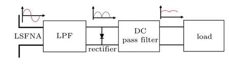
Fig.1.Block diagram of a rectenna as an energy harvesting system.
In the above rectenna system,as shown in Fig.1,the nano-antenna is responsible for receiving the electromagnetic radiation within a particular wavelength and delivering it to the low-pass filter(LPF).So,the matching between the LSFNA and the rectifier is provided by LPF.[50]The LPF blocks the reradiation of higher harmonics produced from the rectification process by the non-linear diode,in which its re-radiation can result in power losses.[51]The diode is the most significant device to perform high energy conversion efficiency.These kinds of rectifiers have to be coplanar and coupled to the LSFN.
Additionally,an impedance matching between the rectenna and the load is needed to transfer the maximum power to the load.It is possible when the load impedance is a conjugation of the rectenna impedance.Finally,the last block DC pass filter between diode and load produces a DC path to the load by dividing the high-frequency parts from the DC signal.[52]The energy conversion efficiency essentially relates to two elements,the LSFNA,and the diode.[51]
In this study,two types of LSFNAs are designed for solar energy harvesting.As shown in Fig.2(b),the LSFNA type-1 consists of a SEDNA with two arms that are made from gold(Au)and nickel(Ni),and similarly,as shown in Fig.3(b),the LSFNA type-2 consists of a SEDNA with Au and titanium(Ti)arms.The SEDNA dimension parameters are defined as length L,width W,and thickness H.As shown in Fig.2(b),four Lshaped nanomaterials make an LSF around the SEDNA.The LSFNA type-1 consists of a Ni LSF,and the LSFNA type-2 consists of an Au LSF.According to this figure,the gap between the LSF and the SEDNA is defined as d.Note that adjusting the gap between the LSF and the SEDNA is very important,and large values of d will decrease the SEDNA and the LSF interaction.The LSFNA dimension parameters are defined as length Lf,width Wf,and thickness Hf.The distance between the nano-antenna arms is indicated with gap width G=Gf.
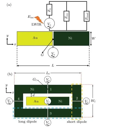
Fig.2.Simplified scheme of(a)the SEDNA,and(b)the LSFNA type-1.
In this analysis,the LSFNA is excited with a linearly polarized plane wave incident on the nano-antenna,and then a voltage difference is generated in its gap.As shown in Fig.2,the receiver nano-antenna can be modeled by a voltage source(voltage difference Vo)and impedance in series(the nanoantenna impedance Za.The rectifier,including the rectifying element(e.g.,a diode)and load.According to Fig.2(b),the LSF consists of four electric dipole nano-antennas with long and short length,which are placed in pairs in front of each other.The long electric dipole length is equal to Lf,and the short dipole length is equal to Wf.As shown in Fig.2(b),these nano-antennas are numbered from 1 to 4.
The circuit model of the nano-antenna is shown in Fig.2,illustrating the input impedance,Zin=Rin−iXin,of the antenna,where we have taken the gap impedance into account,and it is in series with the antenna impedance,Za=Ra−iXa.Note that Zrec=Rrec−iXrecis the rectenna,and Zlis the load impedance respectively.
The type-1(type-2)nano-antenna including a thin NiO(TiO2)insulation layer connecting two Au and Ni(Ti and Au)electrodes with low and high work functions,respectively.As shown in Fig.3,the nano-antenna arms overlap,where a 1 nm thick insulation layer is inserted into the gap area.The insulation layer should be very narrow and less than 4 nm to ensure that the insulator is based only on the tunneling effect.[51]The Au–NiO–Ni(Ti–TiO2–Au)MIM diode has a high difference in the work function between Ni and Au(Au and Ti),which can give rise to a powerful rectifying effect.It is reasonable to obtain some enhancements by increasing the work function difference between the two electrodes.Therefore,the I–V characteristic becomes greatly non-linear,and the connection area of the tunneling junction is decreased.So,a better impedance match is achieved by the LSFNA and diode.Therefore,two types of LSFNA are coupled with a suitable MIM diode.
The harvesting pattern of the antenna array is highly dependent on the geometry of each nano-antenna.The SEDNA has the most straightforward geometry with a very narrow bandwidth.As shown in Figs.2 and 3,the LSFNA is a modified version of the SEDNA,and it is more suitable for energy harvesting.Note that the SEDNA is sensitive to the polarization of the incident wave.Still,as shown in Figs.2 and 3,the LSFNA consists of two perpendicular dipoles in its frame and a SEDNA in its center,which can be assumed as an unpolarized version of the SEDNA.However,as the sun or the other thermal radiations have random polarization,both SEDNA and LSFNA geometries can be used for energy harvesting.But,if the SEDNA is used instead of the LSFNA,on average,almost one-third of the incident energy is absorbed.This is obtained at the advantage of lower area requirements.
As shown in Fig.3,the nano-antenna two metallic strips are placed on top of each other in the gap area.Their length is higher than the surface plasmon decay length at the minimum frequency of the desired band.So,the traveling waves attenuate,and there is no reflection at the open-circuit end of the line.Consequently,these transmission lines have input impedances equaling to their characteristic impedances.The resonance wavelength is limited due to the extensive RC response time and impedance matching to the nano-antenna.[51]So,the LSFNA dimension characteristics(Lf,Wf,Hf)must be optimized to guarantee that the nano-antenna is operating at the desired resonance wavelength ofλres=10µm,15µm,and 20µm.
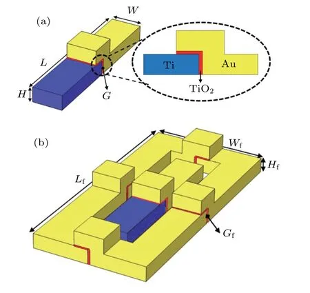
Fig.3.3D scheme of(a)the SEDNA,and(b)the LSFNA type-2.
The nano-antenna resonance wavelength can be determined analytically by using a simple Fabry–Perot model,which analyzes the nano-antenna.[53,54]The Fabry–Perot analytical model is used for studying of geometrical effects and resonance wavelengths of the nano-antenna.In this model,resonance wavelengthλrescan be formulated as

where neffis the effective index of the surface charge wave,Lantis the nano-antenna length,andγis due to the reactance of the nano-antenna ends.[53]Usually,γis of the order of the lateral dimension of the nano-antenna.[53,55]
The resonance wavelength(λres)of a nano-antenna is mainly determined by its dimensions.In this method,PSOA[38]is used to find the best values of nano-antenna dimension,which provides the highest efficiency and the required amount for the input impedance.This manner is performed by combining the PSOA with the FEM,in which the PSOA updates the nano-antenna dimension values and the fitness function evaluation with FE.To study the resonance properties of the LSFNA based on the nano-antenna geometry,it has to use and adjust the geometric parameters to find the best values of the LSFNA dimensions for the impedance matching.The PSOA optimizer investigates the fitness function and finally updates the dimensions of the LSFNA to optimize the fitness function(F)at the LSFNA resonance wavelength(λres).The fitness function of the PSOA is defined as follows:[38]

where S11(in dB)is related to the reflected power of the LSFN,and it is directly associated with the nano-antenna impedance.The a1and a2are weighting factor constants that be chosen to compensate for the change in value between S11andη,so that both parameters have the same effect on the fitness function.The first term tunes the S11to the desired resonance wavelength(λres).The second term should vanish when the fitness function(F)is optimized.So,it guarantees that the LSFNA is at resonance.These constants are selected through an iterative process in which the optimization algorithm is repeatedly running.Then,the values a1and a2are modified after each iteration to optimize both S11andηby using the PSO.
The LSFNA type-1 and type-2 were optimized to have a resonance wavelength atλres=10µm,15µm,and 20µm.The optimization process follows the PSOA to maximize the suggested fitness function(Eq.(2)).In this case,the optimizer works through a 5-dimensional variable solution space(Lf,Wf,Hf,G,d)for the LSFNA.To prevent duplication of content,we only discussed the optimized LSFNA type-2 forλres=10µm.Concerning the optimization of the LSFNA design,the PSOA converged to the maximum amount of fitness function in 80 repetitions.This is shown in Fig.4 with the corresponding values of S11andηat 3 points.

Fig.4.Fitness function values for the LSFNA versus iterations number of the PSOA forλres=10µm.
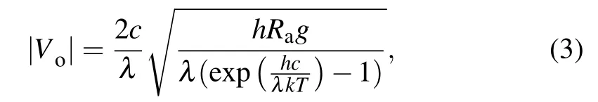
The receiver antenna operating at its resonant wavelength can be modeled by a voltage source Vo=Leff·Einc,and a series impedance,Za.Note that,Leff=Lantsin(θ)is the effective length of the antenna(θis the beam incident angle),Zais the antenna impedance,where Ra=Rrad+Rlossis the antenna resistance,and Xais the antenna reactance,[2]and Eincis the incident radiation electric field amplitude.
where

is the nano-antenna gain,Pang(θ,φ)is the angular power density,Pr(θ,φ)is the angular radiated power of the scattered far-field in a given direction(θandφ),the integral is over all angles,[56]and we assumedλres=λ.
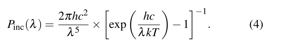
Note that in the solar energy harvesters,Pincis given by Planck’s law for black body radiation as follows:
Also,the power received by the receiving impedance in the RLC circuit can be defined as follows:
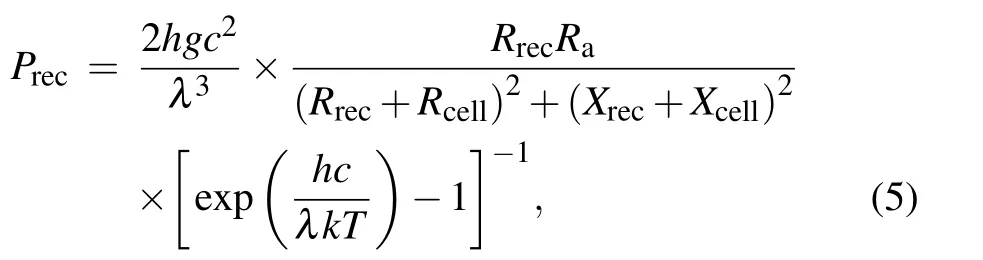
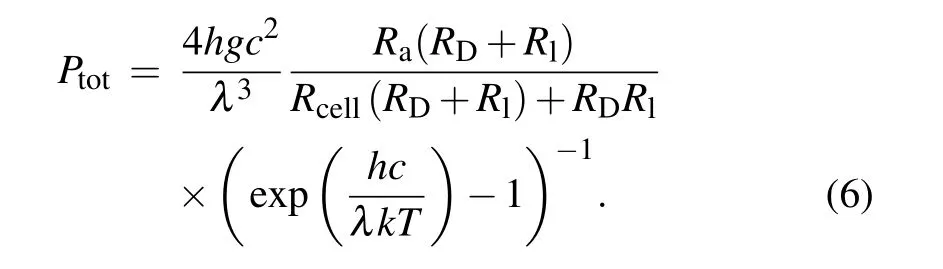
where h is the Planck constant,Rcellis equivalent resistance of the single LSFNA cell,and T is the temperature.The best impedance matching conditions will achieve when the Rrecvalue is much larger than the Raand Rl(the antenna and the load resistance,respectively)values;in contrast,the Raand Rlmust be equal.Also,the total power(Ptot=VoI)in the RLC circuit can be written as follows:
Before starting the studies,the effects of using LSF on the SEDNA should be explained by the equivalent RLC circuit method.[57]The equivalent electrical RLC circuits of the SEDNA and the LSFNA and rectifying system are shown in Fig.5.According to this figure,the SEDNA is shown in a red dashed line,connected in parallel with the LSF equivalent circuit.The LSF equivalent circuit consists of four rectenna connected in series with each other.Fig.6,shows that by utilizing the LSF around the SEDN,four amplifiers are connected to the SEDN.
Figure 5 shows the RLC equivalent circuit of the nanoantennas with the rectifying diode.This rectifier should be coplanar and coupled to the nano-antennas.The MIM tunnel diode with a voltage-dependent resistor(Rrec(V))is modeled in parallel with a capacitor(Crec).Capacitors and inductors can quickly create an impedance matching network.To calculate the impedance matching assumed above,the capacity(Crec)of the diode junction can be ignored because it behaves like a low-pass filter and can only be considered as a DC component.The equivalent resistance of a single LSFNA cell can be defined as follows:

where RSis the SEDNA resistance,Rflis the resistance of the long dipole,and Rfsis the resistance of the short dipole in LSF.

Fig.5.Equivalent circuit of the SEDNA,and the LSFNA.
The current in the circuit can be expressed as follows:

As shown in Fig.6,responsivity S=I′′(Vbias)/I′(Vbias)is a significant property of the rectifier,[32]which is given by the ratio of the first and the second derivatives of the current concerning the bias voltage.Where I′′(Vbias)=d2I/dV2and I′(Vbias)=dI/dV are the first and the second derivatives of the electric current passing along the rectifying diode at a specific bias voltage.Note that in this figure,the calculated dimension values for the LSFNA is 205×50×15 nm atλres=10µm.
Table 1 shows a comparison between the performance of the most advanced MIM diodes with the proposed antenna.According to this table,the previously reported MIM diodes with a high zero bias responsivity suffer from large resistances(MΩ).[29]So,it is hard to match the antenna in this case.On the other hand,the low resistance[32]antenna has a low zero bias responsivity,and therefore shows weak rectification capabilities.However,the proposed antenna gives an excellent performance for both features,high zero bias response,and almost low zero-bias resistance.In addition to the diode’s ability to operate at zero bias,it shows a good rectification ability and offers a lower impedance mismatch with the designed receiver antenna.
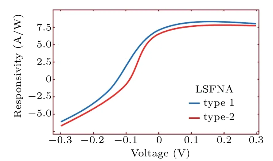
Fig.6.Calculated responsivity of the LSFNA type-1 and type-2 for λres=10µm vs.bias voltage.
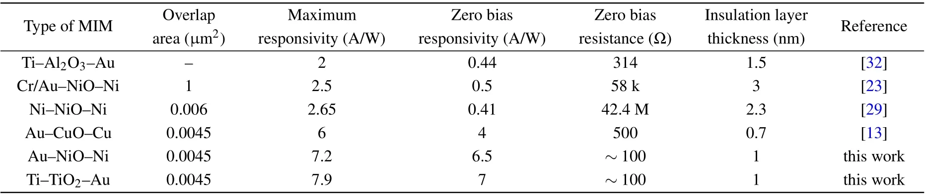
Table 1.Comparison between the proposed antenna MIM diode and the previously reported MIM diodes.
The energy conversion efficiency depends on the nanoantenna and the diode,[51]which indicates the efficiency of the nano-antenna,the impedance matching between the nanoantenna and the rectifier,and the coupling efficiency of the rectifying element to the load.Accordingly,the rectification efficiency is a product of the total harvesting efficiency of each step and defined as follows:[27,58]
The total power supplied by this voltage source is defined by the antenna efficiencyηa.Another efficiency factor is the radiation efficiency(ηr=Rrad/Ra).One of the most critical parts of the total efficiency is the impedance matching between the antenna radiation resistance and the rectifying diode resistance,which is indicated as follows:
Finally,the quantum efficiencyηqshould be considered as follows:[11]

whereωis the angular frequency.Finally,the total harvesting efficiency,which is the ratio of the detected DC power and the incident radiation power,can be described as follows:

The total harvesting efficiency obtained for the SEDNA and the LSFNA is 40.2% and 63.4%,respectively.Note that this study aims to improve the performance of the SEDNA using the LSF at a single wavelength in which the input impedance and field limit are optimized.It is expected that in addition to the enhancement of the radiation characteristics of the SEDNA,they become adjustable under the influence of the LSF.
3.Results
3.1.Nano-antennas specification
In this section,we compared the SEDNA and the LSFNA to investigate the effects of using the LSF on the SEDNA radiation characteristic,such as the near-fields intensity,directivity,and gain.
3.1.1.Near-field intensity and induced current
We investigated the effects of geometrical specifications of the nano-antenna on its radiation characteristics by the FE.The target wavelength range for studying nano-antenna radiation characteristics is selected from 1µm to 30µm.
The incident electromagnetic wave(Einc)stimulates surface plasmon oscillations and causes a high local field in the insolation layer of the rectenna.The local field enhancement factor is defined as follows:[59]
where E(ω)is the wavelength-dependent electric field of the LSFNA coupled with the incident electromagnetic wave.As the wavelength variations,the enhancement factor will reach a maximum amount of Kmaxat the resonance wavelength λres.Figure 8 shows the effects of using the LSF around the SEDNA.The calculated resonance spectra of the local field(K)[59]of two models of the LSFNA is simulated by placing a detector in the origin of the coordinate and plotted according to wavelength.In this figure,K is plotted for the LSFNA with dimensions of(Lf×Wf×Hf)equaling to 205×50×15 nm,which hasλres=10µm.
According to Fig.7(a),using the LSF around the SEDNA caused that all of the resonance wavelengths shifted to the right of the spectrum,and one of the resonant peaks of the SEDNA is shift-out from the target range.Also,the local field enhancement factor of the LSFNA is increased compared with the SEDNA about 6-times.
Figure 7(b)shows the output current of the SEDNA and the LSFNA,where the maximum current Imaxis 2.7 nA for the SEDNA and 8.2 nA for the LSFNA,respectively.Therefore,the maximum current gradually increases with using the LSF.So,because of the increasing local field,which results in more photons absorbed by the dielectric layer,i.e.,higher electromagnetic energy.Accordingly,the excited surface plasmon oscillations induce a higher possibility for electron tunneling,eventually leading to a higher output current.
By comparison between the results obtained in Fig.7 and the results reported in Ref.[24],it can be seen that the local field enhancement factor(K)and the induced current(I)are 2.5-times higher in LSFNA type-1 and 2-times higher in LSFNA type-2 than the bowtie nano-antenna.

Fig.7.(a)The local field enhancement factor and(b)the induced current for the SEDNA,and the LSFNA.
3.2.The hybrid structure of Nano-antenna solar energy harvester device
In this study,we assumed a PSSA,patterned by two types of LSFNA on the SiO2substrate.The proposed energy harvester is depicted in Fig.8.The first layer is divided into two sub-layers with an anti-reflection coating(ARC)layer and an optical micro-lens on top of the PSSA to more power collection and vacuum space.The second layer is a 3 nm chromium thin film(the black layer)used as an adhesion layer.The third layer is a 1.5µm silicon dioxide(SiO2)matching layer,used to increase the transmission of the incoming MIR radiation to the silicon(Si)substrate.The fourth layer is 375µm high resistivity Si(2 kΩ·cm),where the high resistivity reduces the substrate losses.[13]Finally,the fifth layer is a thin copper(Cu)layer with 500 nm thickness placed on the backside of the Si substrate to enhance coupling to the antenna from the substrate.
The optical system is used in the vacuum space to ensure that the incident rays reach the PSSA homogeneously.The incident IR radiation wave illuminates the top layer of the harvesting device,in which the ARC layer decreases the reflected power.Then,the optical micro-lens focuses the IR waves on the PSSA.This optical lens is designed based on what is reported in[40].According to what is reported in[60],an aspheric lens is designed,to reach the field enhancement factor of 106.After the related metal deposition on the oxide,the LSFNA array and the feeding lines are etched to obtain the PSSA.
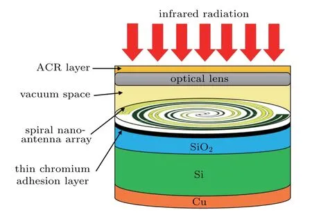
Fig.8.3D scheme of the proposed device structure.
3.3.Design of the PSSA
As shown in Fig.9(a),the PSSA is arranged with a large number of the LSFNAs to create a sufficient field enhancement in the array gap.The PSSA used in this study has two arms,and each arm’s width is increased from the PSSA center to the arm’s end.So,the LSFNA type-1 is used in one arm(the yellow arm)of the array,and the LSFNAs type-2 is utilized in another one(the green arm).Note that the LSFNAs are connected in series with three different sizes,which are designed and optimized forλres=10µm,15µm,and 20µm that placed in sections 1 to 3 in Fig.9(a),respectively,and they are connected in parallel at the two ends of each arm.Also,a sufficient distance is chosen between LSFNAs of different sizes to prevent any interactions between them.Note that by selecting the distance between the elements in order of a multiple of theλres,the field of different LSFNAs is added in phase with each other in the series connection.So,it causes an enhancement effect on the electric field of the PSSA.Also,a parallel connection equals the distance between each LSFNA and the array gap.Therefore,the electric field of different LSFNAs is added constructively,and a wider bandwidth is obtained.One of the proposed design advantages is using different sizes of a nano-antenna in one cell,which reduces the required space for building an array in the electrical circuit.
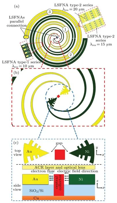
Fig.9.(a)The PSSA layout with three sections that are numbered from 1 to 3,(b)a close sight of the PSSA gap with fractal bowtie nanoantenna,(c)Top view(above)and side view(below)of the PSSA to show rectification process.
According to Fig.9(b),the electrons are emitted from the fractal bowtie nano-antenna tip at a high electric field and move to the central collector in the middle of the structure to produce a rectified current.[40,45]Hence,the field enhancement of a horizontally polarized wave occurs by the resonance of the two horizontal arms of the LSFNA.
As shown in Fig.9(c),the top and side views of the PSSA gap is shown,and it is assumed that the electric field is directed from the right to the left in the gap.So,the electrons are emitted from the left tip to the central collector and absorbed by it.As a result,regardless of the direction of the incident wave,the direction of the induced current is always from the tips toward the central collector.Also,the flat shape of the central collector prevents the field emission from the central collector to the sharp tip.[45]Note that the probability of tunneling from the flat side to the sharp tip is much less than the tunneling probability from the sharp tip to the flat side.So,it causes a rectification of the incident wave.
According to Fig.10,the field emission current.[40]is calculated for 48 element arrays of the LSFNAs.As can be seen,the field emission current spectrum shows that the proposed antenna has a multi-resonance response thanks to the PSSA patterned method.This is an advantage of the proposed antenna compared to the previously reported arrays with only one resonance wavelength pick.[40,45]As expected,the maximum current is achieved atλres=20µm,where the field is maximum.
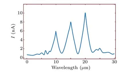
Fig.10.The calculated spectrum of the field emission current with respect to the wavelength.
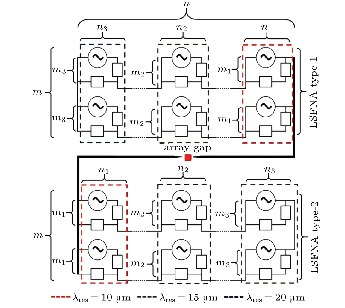
Fig.11.Equivalent circuit of an array of m×n rectennas for each PSSA arms.
The equivalent circuit of the PSSA is shown in Fig.11.Note that in the array form of the antenna,each cell consists of an LSFNA and a rectifier.According to this figure,three sections of each PSSA arms is divided by three dashed lines with red,green,and blue colors,in which each section has mi×niLSFNAs(i=1,2,3).Each cell in this equivalent array circuit corresponds to the circuit in Figs.5 and 12 and each section with numbers i=1,2,3 corresponds to the PSSA layout in Fig.9(a).Also,it is assumed that each arm has m×n rectennas,which m=2×(m1+m2+m3)and n=n1+n2+n3.
Each cell in Fig.11 corresponds to Fig.12,which shows the equivalent circuit,and calculates the output voltage V0achieved when the load is connected to the LSFNA.
By assuming the impedance matching condition between the antenna Zaand the load Zl,the output voltage V0is equal to Vopen/2,in which Vopenis the open-circuit voltage.
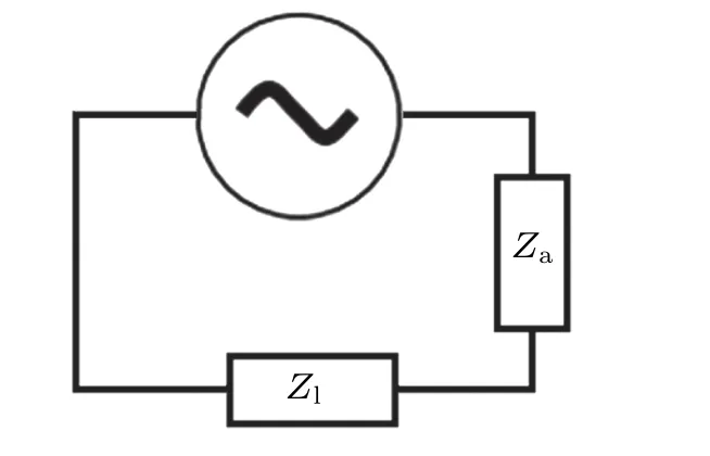
Fig.12.Equivalent circuit for the LSFNA and the output voltage Vo.
The intensity and phase distribution of the electric field verify that the IR radiation energy is concentrated in the dielectric layer due to the coupling effect of the rectenna.Thus,a non-linear effect is observed,which represents the rectification effect in Fig.13.Another feature of the rectifier is its responsivity(Fig.13(d)).According to Fig.13(d),the maximum value is determined to be 2.2 at a DC bias point where the maximum curvature of the I–V curve occurs.So,the rectification effect can be achieved in the proposed antenna with a MIM diode,and the conduction is due to the tunneling of the charge through a thin insulation layer.The obtained results in Fig.13 have a relative agreement with the results reported in Ref.[59]with 4-times enhancement.
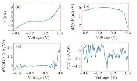
Fig.13.The LSFNA performance,(a)I–V curve,(b)the first derivative(dI/dV),(c)second derivative(d2I/dV2),and(d)responsivity(I′′/I′)vs.bias voltage.

Table 2.Calculated return loss and harvesting efficiency of the proposed nano-antenna.
Note that under ideal conditions,every single cell has an intrinsic ability to harvest the incident solar energy.As shown in Fig.14,the calculated return loss and harvesting efficiency of the proposed nano-antenna is depicted versus the wavelength.The corresponding values of these parameters are written in Table 2.Note that the results are obtained for 24 elements in each arm of the PSSA.As seen in Fig.14(a),the PSSA exhibits return loss values,sorted in Table 3.
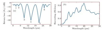
Fig.14.(a)Variation of return loss versus wavelength for 24 elements in each arm of the array,(b)harvesting efficiency.

Table 3.The PSSA return loss values.
3.4.Fabrication possibilities
The most widely used nano-antenna fabrication technique is the electron beam lithography(EBL).This method has high flexibility and accuracy in constructing complex nanoscale structures.[61]However,using this method in the mass production of the nano-antenna is not affordable.Also,due to the production process in this method,the available height of nanostructures is limited to about 50 nm.Therefore,EBL cannot be easily used to produce nano-antennas with high thickness characteristics.[62]Another common lithography technique for nano-antenna fabrication is the focused ion beam(FIB)milling,which is ideal for the production of slot nano-antenna in metal films.Similarly to EB,FIB has significant disadvantages,including very low throughput(typically 10 to 13 m2/s with a high resolution of 30%milling coefficient).[63,64]However,soft lithography can overcome these limitations and various disadvantages of EBL and FIB.[65]Also,it can create arrays with a large area of the nano-antennas with high accuracy.Soft lithography is consisting of a set of patterning techniques that use elastomeric masks(e.g.,polydimethylsiloxane-PDMS)to construct the nano-antenna arrays.[66,67]The softnanolithographic process can be divided into four main steps for large-scale fabrication of the nano-antenna arrays:(1)making a master with nanoscale properties;(2)molding the PDMS mask from the master;(3)creating a photoresist pattern and(4)preparing and assigning a photoresist pattern to the array of the nano-antennas.[68–70]Some low-cost manufacturing methods have already been proposed for a large number of components,which may suffer from manufacturing tolerance.[71,72]For example,simulations show that changing the array gap width by∓25%changes the electric field across the array gap by−9%and+15%,respectively.
In this study,we proposed a novel structure for solar energy harvesting.Our goal at this step is to enhance the antenna radiation characteristics.It is worth noting that the proposed nano-antenna is designed based on the existing substructures for the fabrication of semiconductor components.The fabrication costs can be estimated by using these technologies.For example,we can use prefabricated substrate wafers that can be purchased for an average of§6.Also,due to the planar architecture,simple design of the LSFNAs,by using common material,a low cost design is achieved.For example,Titanium dioxide TiO2is chemically stable,low cost,and abundant,[73]and the PSSA is printed on a low cost dielectric substrate.Semiconductors have also been taken a lot of notice due to their low cost and high conversion efficiency for solar energy.Most solar absorbers are based on silicon(Si)due to their natural abundance and relatively ideal energy bandgap.[74,75]
In general,the fabrication cost of the proposed structure depends on several factors.Among these cases,we can mention the scale of manufacturing,in which the antennas are industrially fabricated or in the laboratory.
4.Conclusion
In this study,we focused on a hybrid structure for thermal energy harvesting based on a nano-antenna array constructed with MIM diodes and the Fowler–Nordheim theory for electron field emission in the array gap.Therefore,an LSFNA studied for the MIR range showed that this nano-antenna could collect radiation emitted from the earth and transmit it to electricity.The LSFNA topology is optimized by PSOA by using FEM,and the best values of the geometrical parameters required for the input impedance of the nano-antenna were found at the resonant wavelengths atλres=10µm,15µm,and 20µm.Also,two types of LSFNA were designed in this study,named by LSFNA type-1 and LSFNA type-2.The type-1(type-2)nano-antenna included a thin NiO(TiO2)insulation layer connecting to two Ni and Au(Au and Ti).The thickness of the insulation layer was 1 nm to ensure that the rectification occurred based on the electron tunneling effect of the MIM diode.Besides,by comparing the simulation results with the nano-antennas previously reported in Table 1,it was shown that the responsivity of the two proposed types of LSFNA is increased.The results showed that by using LSF around SEDNA,not only the local field enhancement factor and SEDNA induction current were increased,but also the resonance wavelength showed red-shift.
Then a PSSA was built by connecting the three mentioned sizes of the LSFNA.The designed PSSA had two arms that were formed by two models of LSFNAs.Each of the PSSA arms included two branches that in each of them,a series connection three sizes of the LSFNA were paralleled to each other.Also,a fractal bowtie nano-antenna was placed on the PSSA gap.So,the rectification of the PSSA was performed with sharp edges in the vacuum and without using diodes based on the Fowler–Nordheim theory.In this manner,the PSSA provided sufficient output current to supply various power consumption applications,and achieved a multiresonance wide-band response.The results showed that the proposed structure can absorb electromagnetic energy in the vicinity ofλres=10µm,15µm,and 20µm.
Also,the detailed results have demonstrated that the I–V characteristic curves of the PSSA validates the rationality of the proposed device.Finally,efficiency calculation was performed to demonstrate the superiority of the PSSA over the previously reported devices.To achieve a multi-resonance wide-band structure,a series of several nano-antennas with different geometrical sizes can be paralleled in the array.In the series connection,the electric field of different nano-antennas was added in phase with each other.Note that the distance between the nano-antennas has to be a multiple of the nanoantenna resonance wavelength.Parallelizing a large number of nano-antennas would also provide enough output current for supplying different energy-consuming applications.The main advantages of the proposed device were great flexibility in the design and relatively high harvesting efficiency with a multi-resonance wide-band response and taking up less space in the electronic circuit.Also,the proposed hybrid structure has an easy implementation process.
杂志排行

Chinese Physics B的其它文章
- Multiple solutions and hysteresis in the flows driven by surface with antisymmetric velocity profile∗
- Magnetization relaxation of uniaxial anisotropic ferromagnetic particles with linear reaction dynamics driven by DC/AC magnetic field∗
- Influences of spin–orbit interaction on quantum speed limit and entanglement of spin qubits in coupled quantum dots
- Quantum multicast schemes of different quantum states via non-maximally entangled channels with multiparty involvement∗
- Magnetic and electronic properties of two-dimensional metal-organic frameworks TM3(C2NH)12*
- Preparation of a two-state mixture of ultracold fermionic atoms with balanced population subject to the unstable magnetic field∗