Direct growth of graphene films without catalyst on flexible glass substrates by PECVD∗
2021-09-28RuiXiaMiao苗瑞霞ChenHeZhao赵晨鹤ShaoQingWang王少青WeiRen任卫YongFengLi李永锋TiKangShu束体康andBenYang杨奔
Rui-Xia Miao(苗瑞霞),Chen-He Zhao(赵晨鹤),Shao-Qing Wang(王少青),Wei Ren(任卫),Yong-Feng Li(李永锋),Ti-Kang Shu(束体康),and Ben Yang(杨奔)
School of Electronic Engineering,Xi’an University of Posts&Telecommunications,Xi’an 710121,China
Keywords:graphene,flexible glass,PECVD,RF power
1.Introduction
Graphene has excellent physical and chemical properties,such as high electrical conductivity and light transmittance.The methods of preparing two-dimensional(2D)graphene include mechanical exfoliation,liquid-phase chemical exfoliation of graphite,[1–3]epitaxial growth,[4]chemical vapor deposition,[5–7]and oxidation-reduction methods.[8,9]The chemical vapor deposition(CVD)has been widely used to synthesize high-quality and uniform graphene films on transition metals,[10]such as copper,[11,12]nickel,[13,14]cobalt,and Pt.[15]However,the CVD-grown graphene on transition metals must be transferred to some insulating substrates for device preparation and performance characterization,which will inevitably cause contamination or defects like wrinkles and cracks.Therefore,the direct formation of graphene on insulating substrates avoids the transfer process and is expected to further improve the quality of graphene films.Recently,Chugh et al.[16]reported the low-temperature growth of graphene at 650°C on non-catalytic SiO2and quartz substrates by using a one-step PECVD process.In 2017,Sun et al.[17]reported the direct preparation of graphene films on soda-lime glass substrates by PECVD at low temperature.Later,Mischke et al.[18]studied the direct growth of graphene on GaN-based light-emitting diodes(LEDs)by PECVD.Most of these studies focused on rigid insulating substrates.Nonetheless,few reports focused on graphene growth on flexible insulating substrates,[19]which is of great significance for flexible transparent electronics.In 2016,Marchena et al.used nickel films on a flexible glass substrate as a catalytic surface to prepare single-layer flexible graphene glass.[20]In 2019,Liu et al.adopted copper foamassisted PECVD to directly prepare graphene on flexible glass and mica.[21]In our work,a simple method is developed to grow graphene films on flexible glass(Corning Willow glass)substrates without metal catalyst.The prepared graphene-on-Willow glass exhibits good electrical and optical properties and has potential applications in transparent flexible electronic devices.
2.Experiment
2.1.Fabrication of graphene films
Graphene films were prepared by a PECVD system(KEJIA Furnace,Zhengzhou,China),which was composed of the following four parts:gas flow control meter,radio frequency(RF)plasma source,heating area,and vacuum system.The schematic diagram and photograph of the experimental setup are shown in Figs.1(a)and 1(b).A quartz tube with an inner diameter of 100 mm was fixed to a double-zone heating furnace.The RF plasma source(13.6 MHz)could continuously output RF power,and the transmitting part of the RF plasma source was composed of coil-type copper material.The 100-µm-thick Willow glass with low surface roughness(<0.5 nm)and high light transmittance(>90%)is used as the substrate and ultrasonically cleaned for 15 min successively in acetone,ethanol,and deionized water to remove impurities from the glass surface.The preparation process is shown in Fig.1(c).The cleaned substrates were loaded into a quartz boat in the center position of the heating region of the PECVD furnace tube.Substrates were firstly heated to the growth temperature(700°C–800°C)in a mixture of argon(100 sccm)and hydrogen(15 sccm)gas atmosphere.When the temperature in the furnace stabilized at the growth temperature,the Ar gas flow was adjusted to 200 sccm.Then,the RF plasma was ignited,and methane(CH4;1 sccm–3 sccm)and hydrogen(8 sccm)were introduced into the tube for growing the graphene on the Willow glass surface for 10 min–150 min.Finally,the Ar and CH4gas flows were switched off,and the H2gas flow was adjusted to 15 sccm.Then,the H2plasma was ignited by RF power of 50 W–350 W to initiate the annealing process and etch the graphene films.After the reaction,the RF power was turned off,and the system was cooled down to room temperature in an Ar/H2gas atmosphere.
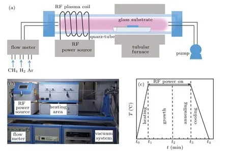
Fig.1.(a)Schematic diagram and(b)optical image of real setup of the PECVD reactor for graphene growing on Willow glass substrate,and(c)graphene preparation process.
2.2.Material characterizations
The surface morphologies of the graphene films were characterized by scanning electron microscopy(SEM;Sigma-500).The chemical elements and their valence states on the surfaces were analyzed by x-ray photoelectron spectroscopy(XPS;Thermo Fisher 250Xi,USA).Structures and morphologies of the graphene films were analyzed by high-resolution transmission electron microscopy(HR-TEM;JEOL JEM-2100F).Raman spectra were obtained with a 532-nm laser as the excitation light source for frequency shifts in a range from 1000 cm−1to 3000 cm−1.The light transmittance of the film was measured by UV-Vis spectroscopy(Shimadzu UV-2300).I–V curves of the thin films were measured by an electrochemical workstation(Shanghai Chenhua,CHI1000C).The electrical properties of the graphene films were determined using a non-contact hall tester(LEI1600).
3.Experimental analysis of growth mechanism
Figure 2 shows the schematic diagram of the graphene growth on flexible Willow glass by PECVD.Willow glass is an amorphous material with completely different chemical bonds and lattice structure from graphene,causing serious lattice mismatch and thermal mismatch between graphene and Willow glass.[22,23]At the initial stage,the impact dissociation of high-energy electrons on methane and a small amount of dehydrogenation reaction decomposes methane into active substances such as CHx,C2Hy,and atomic C and H.These active substances are adsorbed on the glass at growth temperatures of 700°C–800°C,and a horizontal carbon buffer layer is introduced to release the internal stress between graphene and Willow glass.[24]With increasing growth time,the carbon layers evolve,showing an upward growth trend and extend over the entire Willow glass surface.

Fig.2.Schematic diagram of graphene growth on flexible Willow glass.
4.Results and discussion
Previous studies have shown that the surface treatment of graphene films with hydrogen plasma can effectively improve the photoelectric properties.[25,26]Unlike the traditional annealing and hydrogen plasma etching,a new method is used to treat the prepared graphene film:the temperature is kept at a growth temperature of 700°C–800°C,and H2flow and RF power are set to be 15 sccm and 300 W,respectively.Residual CH4in the furnace continues to decompose into CHx,C2Hy,and atomic C and H under the etching of H plasma at high temperature.
Methane dehydrogenation with the formation of(CH3)∗radical(CH4→(CH3)∗+H∗)should overcome a 1.6-eV(~16kT at 1000°C)activation barrier,which leads to a ratelimiting step hindering graphene from growing in the absence of additional catalysts such as hydrogen.[27]Hydrogen plasma serves as either an activator of carbon on the substrate or an etching reagent that changes the thickness and defects of graphene on Willow glass.[28]The addition of H2results in excited hydrogen atoms(H∗)by the following reaction:

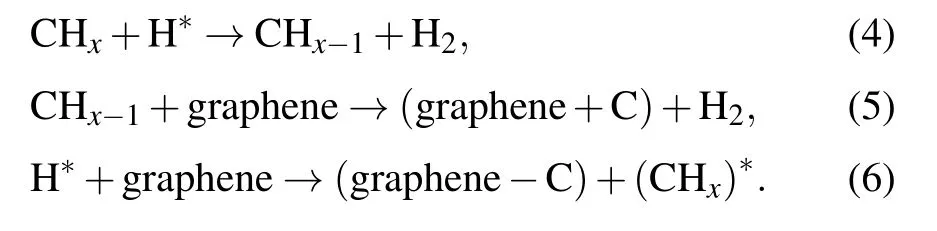
At that time,a large number of excited H atoms are sufficient for dehydrogenating the methane through reactions(4)and(5).The dissociation mechanism of methane is dominated by the impact of energetic electrons(“physical reaction”)and the dehydrogenation effect of hydrogen(“chemical reaction”).Moreover,hydrogen plasma can etch the defects and amorphous carbon produced during the growth of graphene according to reaction(6)[31]
The Raman spectra of graphene-on-Willow glass before and after etching by hydrogen plasma are shown in Fig.3(a).The Raman signal of graphene without etching exhibits a small 2D peak and broad peaks,suggesting a low completeness and crystallization degree.[32]After being etched by H plasma,the samples exhibit three distinct Raman peaks at around 1350 cm−1(D peak),1580 cm−1(G peak),and 2700 cm−1(2D peak),respectively.The sharper G peak implies a better crystallization of graphene after H plasma etching.The I–V(current–potential)curves of the samples are shown in Fig.3(b).The I–V slope of the sample before being etched is smaller than that after having been etched by H plasma.The above results clearly show that the graphene films etched by H plasma are beneficial to the improvement of the quality and electrical properties of the samples.
In order to obtain flexible graphene-on-glass samples with better quality,it is necessary to optimize the processing factors of graphene.The key factors include RF power,gas flow rate,growth time,and growth temperature.The quality of the sample is analyzed mainly by Raman spectroscopy.The Raman spectra of graphene/Willow glass samples prepared under different methane gas flow rates are shown in Fig.4.The growth temperature is fixed at 750°C for 100 min,and the H2/Ar ratio is 8/200 sccm.Figure 4(a)shows clear D band,G band,and 2D band peaks of the graphene/Willow glass samples.The relationships between ID/IG(black curve,the ratio between the intensities of D and G peaks)and grain size La(blue curve)of samples prepared at different methane gas flow rates are shown in Fig.4(b).In addition,the grain size Laof the graphene/Willow glass is calculated from the Tuinstra–Koeing relation[33]

Figure 5 shows the Raman spectra of graphene/Willow glass samples prepared at different growth times in a range from 30 min to 150 min.The growth temperature is fixed at 750°C for 300 W with CH4/H2/Ar gas flow rates of 2.0/8.0/200.0 sccm,respectively.When the growth time is less than 30 min,no Raman peak is observed.The ID/IGratio decreases with the increase of the growth time from 30 min to 100 min.Figure 5(c)shows the variation of the I2D/IGratio with growth time.The I2D/IGratio is around 0.5–0.8,which indicates that the graphene nanowall probably consists of multiple layers.Based on the Raman data of these samples,the growth time is set to be the optimized value of 100 min in the following experiments.
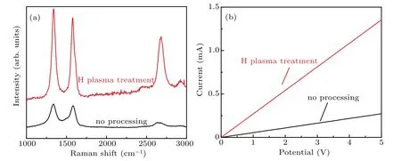
Fig.3.(a)Raman spectra and(b)I–V curves of graphene-on-Willow glass samples before and after hydrogen plasma treatments.
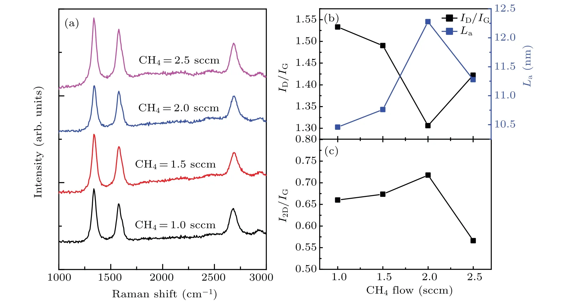
Fig.4.(a)Raman spectra of graphene films prepared at different methane gas flow rates(1.0,1.5,2.0,and 2.5 sccm)grown on Willow glass;(b)ID/IG ratio(black curve)and grain size La(blue curve)varying with methane gas flow rate;(c)curve of I2D/IG varying with methane gas flow rate.
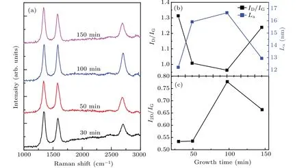
Fig.5.(a)Raman spectra of graphene films on Willow glass,prepared at different growth times(30,50,100,and 150 min);(b)ID/IG ratio(black curve)and grain size La(blue curve)varying with growth time;(c)I2D/IG versus growth time.
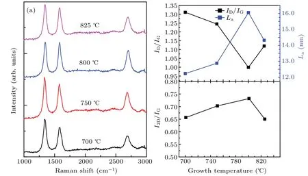
Fig.6.(a)Raman spectra of the graphene films on Willow glass substrates grown at different temperatures(700,750,800,and 825 °C);(b)ID/IG ratio(black curve)and grain size La(blue curve)varying with growth time;(c)I2D/IG versus growth temperatures.
The effects of the growth temperature on the quality of graphene grown on willow glass are shown in Fig.6.With growth temperature increasing from 700°C to 825°C,the ID/IGpeak intensity ratio decreases.As the willow glass substrate melts at temperatures above 825°C,800°C is identified as the optimal growth temperature for yielding the lowest ID/IGpeak intensity ratio where the willow glass substrate is still stable.Therefore,800°C is used as the optimal growth temperature to improve the fraction of sp2C=C bonds and reduce the number of defects in the film.
As shown above,the optimized experimental parameters are a growth time of 100 min and mixed CH4/H2/Ar gas flow rates of 2.0/8.0/200.0 sccm,respectively.
Figure 7 shows the macro and micro surface morphologies of the graphene films on the Willow glass substrates prepared at different values of RF powers ranging from 200 W to 300 W.Figure 7(a)shows the macroscopic morphology of the flexible Willow glass substrate(10 mm×10 mm)without and with the graphene film,revealing that all the films are homogeneous and have neither cracks nor holes.The transparency for each of the samples decreases with the augment of RF power,corresponding to an increase in the graphene film thickness.Higher RF power supports the completion of the cracking reaction of methane in the furnace,resulting in the obtainment of thicker graphene films on the substrates.Figures 7(b)–7(d)show the micrographs of the graphene films prepared at different values of RF power,revealing the microscopic surface morphologies.Figure 7(e)shows that a buffer layer is formed on the substrate surface in the initial stage,and that a small number of vertical graphene nanowalls appear on this buffer layer.With the increase of RF power,the nanowalls extend over the entire Willow glass surface due to the improved degree of gas ionization.The RF power determines the ionization degree of gas molecules in the furnace,which in turn affects the densities and activities of different species,such as high-energy electrons,ions,and atoms,in the reaction chamber.The buffer layer is a distinct 15-nm-thick layer between vertical graphene and the substrate and is composed of amorphous carbon and graphite as shown in Fig.7(e).
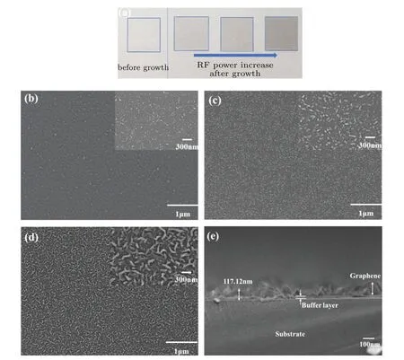
Fig.7.(a)Macroscopic surface morphologies of graphene films,(b)–(d)micrographs of graphene/Willow glass substrates prepared at different values of RF power(b)200,(c)250,and(d)300 W showing microscopic surface morphologies;(e)cross-sectional SEM image of graphene-Willow glass with RF power of 300 W.
Figures 8(a)and 8(b)show the XPS analysis of the graphene/Willow glass sample surfaces.Figure 8(a)shows the XPS survey spectrum,which contains the C 1s peak at 284.5 eV and O 1s peak at 531.4 eV.The atomic fractions of various elements are calculated from the XPS survey spectrum and found to be 95.23% and 4.77% for C 1s and O 1s,respectively.The existence of O1s peaks might be due to a small amount of oxygen adhering to the quartz tube wall and because of silicon hydride bond fracture as well.The high-resolution C 1s spectrum of graphene/Willow glass shown in Fig.8(b)is deconvoluted into three components,including the sp2C=C peak at 284.5 eV(80.94 %),sp3C–C peak at 285.3 eV(15.28%),and C–O peak at 286.2 eV(3.78%).[34]The sharp peak is predominantly related to the sp2carbon bond,[35]which confirms that the synthesized material has a graphene structure.[36]Structure and morphology of the graphene/Willow glass are characterized by HR-TEM and from the corresponding selected-area electron diffraction(SAED)pattern.The HR-TEM image in Fig.8(c)reveals that the graphene film has an interplanar spacing of 0.35 nm.The inset of Fig.8(c)shows a clear diffraction ring pattern with spots,which indicates a polycrystalline structure due to interlaced grain boundaries,stitched grain patches in various orientations,or many layers.[37–39]The HRTEM image of the graphene/Willow glass in Fig.8(d)shows that the prepared graphene films are composed of less than 10 layers of graphene.The corresponding 2D and three-dimensional(3D)AFM images confirm the vertically oriented morphologies of the graphene nanowalls grown on the flexible Willow glass.
The XRD is a common characterization method for the analysis of crystal structures of materials.Different diffraction peaks indicate the integrity and disorder of the spatial arrangement of the graphene sheets,respectively.Figure 8(e)shows the x-ray diffraction pattern of the graphene/Willow glass sample,revealing a single sharp peak at 26.381°,which is assigned to the(002)plane.Based on the Bragg’s law,the crystal plane spacing of the graphene film is obtained to be 0.338,which is consistent with the previously reported values.[40]A broad peak at around 10°may be attributed to the disordered graphene film.

Fig.8.(a)XPS survey spectrum,(b)C 1s high-resolution deconvolution peak spectra,(c)HR-TEM image and SAED pattern(inset image),(d)HR-TEM image(showing vertical graphene nanosheets),and(e)XRD pattern of graphene/Willow glass.
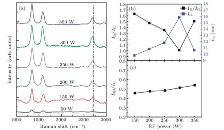
Fig.9.(a)Raman spectra of the graphene films on Willow glass prepared at different values of RF powers(50,100,150,200,250,300,and 350 W);(b)ID/IG ratio(black curve)and grain size La(blue curve)versus RF power;(c)I2D/IG ratio versus RF power.
Raman spectroscopy is one of the most prominent ways to determine the quality of graphene films.[18]Raman spectra of the graphene/Willow glass samples prepared at different values of RF power are shown in Fig.9(a).When the RF power is 50 W,the D and G peaks are weak,and the 2D peak is negligible,indicating that only amorphous carbon clusters and graphite were deposited on the Willow glass surface.When the RF power increases from 50 W to 350 W,obvious 2D peaks appear.At low RF power,the formation of amorphous carbon film is favored in comparison with that of graphene films.With the increase of the RF power,the 2D peak position of graphene is blue-shifted slightly,which is attributed to the decrease of the Fermi level velocity of the phonon dispersion and the change of the phonon dispersion curve caused by the superposition of multilayer graphene.The variation of ID/IG(black curve)and grain size La(blue curve)with RF power are shown in Fig.9(b).
The grain size Lahas a negative correlation with the defect intensity ratio ID/IG.The ID/IGratio decreases from 1.63 to 1.00 when the RF power increases from 150 W to 300 W,indicating the enhanced crystallinity of the graphene film.The ID/IGratio can reach only about 1.00,which may be due to the edge gap between the upward graphene nanowalls.When the RF power is higher than 300 W,the ID/IGrises again.This may be due to the fact that when the RF power is too high,the carbon atoms are deposited too fast,and amorphous carbon atoms are agglomerated easily,resulting in a decrease in film quality.Figure 9(c)shows the variation of I2D/IGwith the RF power.The I2D/IGratio is around 0.5,indicating that the graphene nanowalls are composed of multiple layers,which is consistent with previous TEM analysis.
The optical and electrical properties of graphene/Willow glass are measured.Figure 10(a)shows the curves of light transmittance versus wavelength of the graphene samples at different values of RF power,which decrease with RF power increasing.The current–voltage(I–V)curves of graphene-Willow glass are shown in Fig.10(b),indicating that the I–V slopes of the samples increase almost linearly when the RF power increasing from 50 W to 300 W.However,the slope decreases when the RF power is 350 W.This indicates that the conductivity of the graphene sample is improved as the RF power increase from 50 W to 300 W,while it decreases when the RF power is higher than 300 W,which is in agreement with the conclusion from previous analysis.
The electrical properties of graphene are investigated using a non-contact hall tester.The mobility of ordinary semiconductors is usually around 102cm2/(V·s)–106cm2/(V·s).Carriers in semiconductors are scattered mainly by defects and impurities at low temperatures.The carrier mobilities of the prepared graphene–Willow glass samples are much lower than those of monolayer graphene samples,which is probably due to the defects caused by discontinuities in the 3D graphene nanosheets and impurities generated during growth.According to the Hall effect,the Hall coefficients of p-type semiconductors are positive,and those of n-type semiconductors are negative.Therefore,the prepared graphene/Willow glass samples are identified as p-type doping.As shown in Table 1,the mobility decreases with carrier concentration increasing.The sheet resistance is less than 1 kΩ/sq,but it has a minimum value at 279.61Ω/sq.
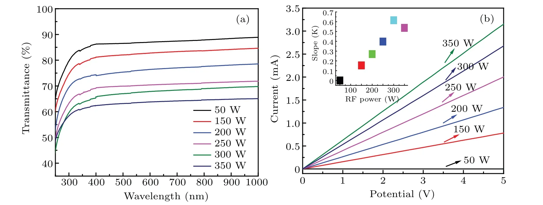
Fig.10.(a)Variations of light transmittance with wavelength of the graphene/Willow glass sample prepared at different values of RF powers;(b)I–V curves of the graphene/Willow glass sample prepared at different RF powers.

Table 1.Photoelectric properties of graphene/Willow glass samples prepared at different values of RF power.
5.Conclusions
In summary,graphene films on a flexible Willow glass substrates are successfully prepared by a designed direct PECVD approach.The photoelectric properties and surface morphologies of the graphene–Willow glass can be adjusted by varying the growth parameters.In this paper,the influence of the RF power on the growth of graphene on flexible Willow glass is studied systematically,revealing that the RF power is an important parameter to modulate the photoelectric properties and surface morphology of graphene–Willow glass.The density and thickness of the graphene nanosheets on Willow glass increase significantly with the increase of the RF power.The 2D Raman peak intensity and the I–V slope of the graphene film increase as the RF power increases from 50 W to 300 W.The light transmittance increases with the augment of the RF power.However,when the RF power exceeds 300 W,the properties of the graphene–Willow glass degrade.The non-catalytic direct synthesis of graphene is one of the keys to the industrial production of flexible graphene devices.Therefore,our research is of great significance in developing transparent flexible electronics.
杂志排行

Chinese Physics B的其它文章
- Multiple solutions and hysteresis in the flows driven by surface with antisymmetric velocity profile∗
- Magnetization relaxation of uniaxial anisotropic ferromagnetic particles with linear reaction dynamics driven by DC/AC magnetic field∗
- Influences of spin–orbit interaction on quantum speed limit and entanglement of spin qubits in coupled quantum dots
- Quantum multicast schemes of different quantum states via non-maximally entangled channels with multiparty involvement∗
- Magnetic and electronic properties of two-dimensional metal-organic frameworks TM3(C2NH)12*
- Preparation of a two-state mixture of ultracold fermionic atoms with balanced population subject to the unstable magnetic field∗