Phase transition-induced superstructures ofβ-Sn films with atomic-scale thickness∗
2021-09-28LeLei雷乐FeiyueCao曹飞跃ShuyaXing邢淑雅HaoyuDong董皓宇JianfengGuo郭剑锋ShangzhiGu顾尚志YanyanGeng耿燕燕ShuoMi米烁HanxiangWu吴翰翔FeiPang庞斐RuiXu许瑞WeiJi季威andZhihaiCheng程志海
Le Lei(雷乐),Feiyue Cao(曹飞跃),Shuya Xing(邢淑雅),Haoyu Dong(董皓宇),Jianfeng Guo(郭剑锋),Shangzhi Gu(顾尚志),Yanyan Geng(耿燕燕),Shuo Mi(米烁),Hanxiang Wu(吴翰翔),Fei Pang(庞斐),Rui Xu(许瑞),Wei Ji(季威),and Zhihai Cheng(程志海)
Beijing Key Laboratory of Optoelectronic Functional Materials&Micro-nano Devices,Department of Physics,Renmin University of China,Beijing 100872,China
Keywords:epitaxial growth,β-Sn films,bilayer-by-bilayer,superstructures,structural transition,scanning tunneling microscopy,surface energy
1.Introduction
Since the discovery and characterization of graphene,[1,2]the novel two-dimensional(2D)materials,especially for monoelemental 2D materials,have been the subject of an increasing area of research due to their exotic non-trivial topological properties and potential applications.[3–10]In the periodic table,most of 2D monoelemental materials,consisting of the elements in the main group of IIIA,IVA,and VA,have been successfully prepared,such as borophene,[11–14]silicene,[15–17]antimonene,[18–21]bismuthine,[5,22,23]and so on.[24–26]Among them,the 2D materials consisted of heavy elements have been predicted as topological insulators with enhanced bulk gap and nontrivial edge state due to their strong spin–orbit coupling(SOC).[27–29]For instance,the bismuthine grown on SiC(0001)substrate shows a large gap of~0.8 eV and conductive edge states.[23]The ultraflat stanene on Cu(111)exhibits a topological bandgap(~0.3 eV)induced by SOC at theΓpoint.[30]The robust one-dimensional topological edge state of antimonene monolayer has been also observed experimentally.[31]
It is well known that bulk Sn exhibits two kinds of phases.[32]The one is semiconductingα-Sn with diamond structure at low temperature,while the other one is metallic β-Sn at high temperature,which has a body-centered tetragonal(bct)structure.The bulk Sn undergoes a phase transition fromβ-Sn toα-Sn at 285 K upon cooling process.[33]The monolayerα-Sn(111)with honeycomb structure,known as stanene,has been theoretically predicted to be a topological insulator with nontrivial edge states.[28,34]The stanene has been further successfully prepared by molecular beam epitaxy(MBE).[30,35]In recent years,the search for Majorana bound states(MBSs)in condensed matter systems has attracted a great deal of interests for potential applications in topological quantum computing.[36–40]The bulkβ-Sn is a typical superconductor below 3.72 K.[41]The further theoretical exploration points out that the ultrathinβ-Sn(001)is an ideal platform for topological superconductor(TSC)with MBSs.[42]Recently,the strainedβ-Sn(001)thin films were obtained via phase transition engineering by leaving the fcc-Sn(111)at room temperature for some weeks.[43]Theα-Sn thin films can also transform into strainedβ-Sn films with the increase of thickness because of the large lattice mismatch and symmetry difference.[32,44]The one-step growth and the detailed structural characterization of ultrathinβ-Sn films are still lacking.

2.Materials and methods
The sample preparation and STM/AFM measurements are described below.Theβ-Sn thin film was grown on freshly cleaved highly oriented pyrolytic graphite(HOPG)substrates by standard MBE in ultra-high vacuum(UHV)chamber under a base pressure of 3.0×10⁻¹⁰Torr(1 Torr=1.33322×10²Pa).The HOPG substrate was cleaved in air and immediately loaded into the MBE chamber,then annealed at 773 K overnight to remove contaminants.High purity Sn(99.999%)was evaporated from the Knudsen cell onto the HOPG kept at~500 K.After the growth experiment,the sample was first transferred to another UHV chamber with LTSTM(PanScan Freedom,RHK)for the following STM measurements.The low temperature STM measurements were performed at 9 K with chemical etched W tip calibrated on a clean Au(111)surface.All STM images were processed by Gwyddion and WSxM software.[45]The AFM measurements were performed on a commercial AFM system(MFP-3D Infinity,Asylum Research),in combination with a dynamic signal analyzer(HF2LI,Zurich Instruments)in the atmosphere circumstance.
3.Results and discussion
Bulk Sn is allotropic with two stable phases of whiteβ-Sn and grayα-Sn,and undergoes the structural phase transition at 286 K.The bulkβ-Sn has a body-centered tetragonal(bct)structure(A5,space group I4/amd)with lattice constants of a=5.82˚A and c=3.18˚A,as shown in Fig.1(a).Figure 1(c)illustrates the diamond crystal structure of bulkα-Sn(a=6.49˚A,space group Fd3m).Figure 1(b)shows the bilayer structural model ofβ-Sn with double unit cells.The number 8 of Sn atoms in a unit cell ofα-Sn is identical with that of double unit cells ofβ-Sn,which could play important roles in the structural phase transition ofα-βSn.In bulk Sn,this phase transition is well known as tin pest[46]due to the powdering ofα-Sn fromβ-Sn when cooling.The volume of α-Sn(273˚A3/unit cell)is pronouncedly larger than that of β-Sn(216˚A3/double unit cell),which results in a~26%volume increase of phase transition fromβ-Sn toα-Sn.The bulk Sn occurred during phase transition is so structurally weak that readily crumbles into powder due to huge internal compressive strain.While the structural phase transition behavior of Sn films with atomic-scale thickness is still not clear,which may play important roles in determining their morphology,structures and properties significantly.
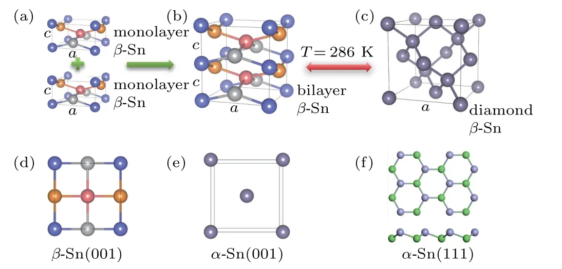
Fig.1.Atomic structural models and phase transition of Sn.(a)and(b)Atomic structural models of monolayer(a)and bilayer(b)β-Sn(bct structure,white tin),respectively.(c)Atomic structural models ofα-Sn(diamond structure,grey tin).(d)Top view of atomic structure ofβ-Sn(001)surface.(e)Top view of atomic structure ofα-Sn(001)surface.(f)Top view(upper)and side view(lower)of atomic structure ofα-Sn(111)surface.Bulk tin undergoes a structural phase transition ofα-Sn toβ-Sn at~286 K.
As we know,the Sn belongs to the elements of group IVA in the periodic table.Among of the elements of group IVA,C,Si,and Ge exhibit strong semiconducting property due to they have a tendency to form covalent diamond structure by strong sp3hybridization at ambient conditions.[47]The sp3hybridization becomes weaker as the atomic number increases in the elements of group IVA.The heavy element Pb shows a metallic fcc structure due to the prohibition of formation of sp3bonds.The position of Sn in the elements of group IVA is the borderline between light elements(C,Si,and Ge)and heavy element(Pb).Therefore,the covalent diamond structure ofα-Sn is relatively weak at low temperature[48]with zero-gap semiconducting property.Theβ-Sn is stable and metallic at high temperature due to the metallic bonding nature in body-centered tetragonal crystal structure.
For ultrathin Sn film,it is clear that the surface structure and stability of ultrathin Sn film will pronouncedly affect the structural phase transition behaviors.The(001)surfaces of β-Sn films andα-Sn films are relatively stable with similar fourfold symmetric structure,as shown in Figs.1(d)and 1(e).The surface atoms ofα-Sn(001)surface is flat and more closepacked than that ofβ-Sn films.Therefore,it can be speculated that theβ-Sn(001)surface has a tendency to transform intoα-Sn(001)surface by the upward moving of central pink Sn atom to reduce the surface corrugation and surface energy.Theβ-Sn(001)surface of Sn films still have a tendency to further transform into the most stable and close-packed(111)surface ofα-Sn films with threefold symmetric structure.It is clear that the above surface transformation will introduce significantly interval in-plane compressive strain within the ultra Sn films,which may affect their surface morphology and lattice structures.
The high-qualityβ-Sn films were successfully synthesized on HOPG,and further characterized by AFM and STM.Figure 2(a)shows a large-scale AFM topography images of the as-prepared Sn films with lateral sizes of~600 nm–800 nm.It seems that the Sn nanofilms were made of many merged small islands and represent a multi-domain crystalized structure.Figure 2(b)shows the typical large-scale STM topographic image of Sn nanofilms,in which the merged small islands with uniform thickness are clearly resolved in the Frankvan der Verwe(layer-by-layer)growth mode.
Figure 2(c)shows the high-resolution STM image of Sn films with many step edges.The surface of Sn films was smooth and flat,suggesting their high crystallinity.Unexpectedly,all the step heights of Sn films are~0.6 nm,as shown in Fig.2(d),which is consistent with the bilayer height ofβ-Sn films.More line profiles are supplied in Fig.S1 to indicate the exclusive step heights of bilayer.As shown in Figs.1(b)and 1(c),the bilayer-by-bilayer growth mode of Sn films at here should be related with the similarity of unit cell for theα-Sn monolayer andβ-Sn bilayer during the structural transition of β-Sn toα-Sn.
The multi-domain structures of Sn nanofilms were further clearly resolved,as shown in the STM topography and corresponding current images of Figs.2(e)and 2(f).The various domains were only vaguely observed in the topographic images due to their very small apparent height difference,while can be clearly resolved in the current images via their different long-range ordered surface structures.The apparent height difference between the domains is far less than the thickness(~0.32 nm)of monolayerβ-Sn(001)monolayer,as shown in Figs.2(g)and 2(h).More STM images of Sn nanofilms with multi structural domains were supplied in Fig.S2.

Fig.2.Epitaxially growth of theβ-Sn films on HOPG substrate.(a)AFM morphology image of Sn films.(b)Large-scale STM topographic image of Sn films.(c)High-resolution STM topographic image of the Sn films.(d)Line profile taken along the black line in panel(c).The bilayer-by-bilayer growth mode of Sn films is confirmed by the step heights of~0.6 nm.(e)and(f)STM topography(e)and corresponding current(f)images of Sn films.The various structural domains were clearly resolved within the Sn films and highlighted with the domain walls marked by blue dashed lines.(g)High-resolution STM image with domains.(h)Line profile taken along the black line in panel(g).The small topography difference is observed between different domains of Sn films.(b)V=1.6 V,I=200 pA;(c):V=−2.4 V,I=−300 pA;(e)–(f):V=1.8 V,I=100 pA;(g):V=−0.8 V,I=−200 pA.
The high-symmetric superstructures of the domains within theβ-Sn films were first carefully investigated via the high-resolution STM images.Figure 3(a)shows the atomically resolved STM image of the domain with the flat surface atoms and smallest(1×1)square lattice.The corresponding unit cell(marked with red solid square)is measured to be 0.41 nm×0.41 nm,which is not consistent with the pristine surface structure ofβ-Sn(001)in Fig.1(d).If the central pink Sn atoms ofβ-Sn(001)move upward to form the flat and close-packed(001)surface to reduce the surface energy,the arrangement of surface Sn atoms in the surface will be almost identical with those in Fig.3(a),as shown by the schematic modes of Fig.3(i).Actually,this unique flat surface structure in Fig.3(a)is very similar to theα-Sn(001)surface in Fig.1(f),
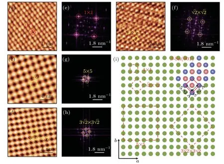
Fig.3.High-symmetric superstructures of the domains within theβ-Sn nanofilms on HOPG substrate.(a)–(d)Atomic-resolution STM images of theβ-Sn domains.The unit cells are marked with red and yellow solid squares.(e)–(h)The corresponding FFT images of panels(a)–(d),respectively.(i)Schematic models of the observed surface superstructures.The green spheres represent the surface Sn atoms,and the theoretical atomic structure ofβ-Sn(001)surface is shown at the top right corner.(a)V=1.7 V,I=200 pA;(b)V=0.6 V,I=200 pA;(c)V=2.7 V,I=50 pA;(d)V=2.5 V,I=100 pA.
Finally,the bilayerbybilayer growth mode and various superstructures of the epitaxialβ-Sn films are phenomenally discussed based on the structural transition ofβ-Sn toα-Sn at the two-dimensional limit.Firstly,the tentative structural transitions ofβ-Sn toα-Sn films adopt the whole bilayer transform due to their identical number of Sn atoms,as shown in Figs.1(b)and 1(c).Secondly,the first step of structural transition is the surface transformation ofβ-Sn(001)toα-Sn(001)by moving the central Sn atom upward to get the flat surface and reduce surface energy.In this step,the(001)surface of theβ-Sn films provides the most convenient relaxation mechanism for the structural transition,while the fourfold symmetry and size of the surface unit cell are still preserved.Thirdly,the high-symmetric superstructures with large square unit cells were formed with large surface corrugations(as shown in Fig.S5)to release the significant internal compressive strain during the further structural transition.In this step,the fourfold symmetry of the Sn films is still preserved,while the translation symmetry is reduced with large supercells of similar size.Fourthly,the above fourfold-symmetric superstructures were further distorted to tentatively transform into the most stable and close-packedα-Sn(111)surface with threefold symmetry.In a word,the epitaxial growth of ultrathinβ-Sn films is realized on the inert HOPG substrate.The Sn films stay long enough at room temperature and low temperature.However,the complete transition fromβ-toα-Sn was not observed.Theβ-Sn films have a trend to transform intoα-Sn films at low temperature.The unique arrangement of surface Sn atoms in the surface and multiple superstructures observed in our experiments were introduced due to the structural phase transition trend fromβ-Sn toα-Sn films at low temperature at the two-dimensional limit.
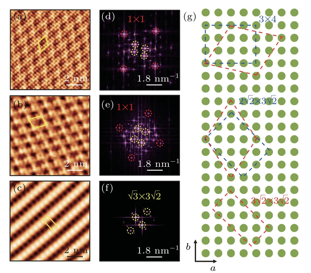
Fig.4.Distorted superstructures of the domains within theβ-Sn films on HOPG substrate.(a)and(b)High resolution STM topography images of two distorted superstructures with parallelograms superlattice.The super cells are marked with the yellow solid parallelograms.(c)High-resolution STM image of striped superstructure with rectangular superlattice marked by the yellow solid rectangle.(d)–(f)The corresponding FFT images of panels(a)–(c),respectively.(g)Schematic illustrations of distorted[(a)and(b)]and striped(c)superstructures.The red dashed parallelograms represent distorted superstructures from the superstructures with rectangular superlattice marked by the blue-dashed rectangles.(a)V=2.2 V,I=100 pA;(b)V=0.4 V,I=300 pA;(c)V=1.9 V,I=200 pA.
The electronic properties of the Sn films were further investigated by the scanning tunneling spectroscopy(STS)measurement.The similar dI/dV spectra taken at various structural domains is shown in Fig.S4 with finite local density of states(LDOS)at the Fermi energy(EF),indicating the metallic property of the Sn films.This result is consistent with the band structure of theβ-Sn films calculated by density functional theory(DFT).[42]The ultrathin Sn films with various superstructures could exhibit interesting modified superconductive and topological properties,which will inspire more experimental and theoretical work on this idea platform for topological superconductivity.
4.Conclusion
In summary,we have successfully grown ultrathinβ-Sn(001)films on HOPG substrates and systematically explored various superstructures observed in ultrathinβ-Sn(001)films.We confirm thatβ-Sn(001)films growth with a bilayer-bybilayer growth mode.The further study found that there are various domains in theβ-Sn(001)films.The long-range ordered superstructures in different domains,including highsymmetric and distorted superstructures,were systematically characterized.We assume that these superstructures are induced via structural phase transition ofβ-toα-Sn at the twodimensional limit.Our study not only demonstrates the importance of the structural phase transition during the formation of superstructures ofβ-Sn,but also opens a door for studying topological properties ofβ-Sn thin films in the future.
杂志排行

Chinese Physics B的其它文章
- Multiple solutions and hysteresis in the flows driven by surface with antisymmetric velocity profile∗
- Magnetization relaxation of uniaxial anisotropic ferromagnetic particles with linear reaction dynamics driven by DC/AC magnetic field∗
- Influences of spin–orbit interaction on quantum speed limit and entanglement of spin qubits in coupled quantum dots
- Quantum multicast schemes of different quantum states via non-maximally entangled channels with multiparty involvement∗
- Magnetic and electronic properties of two-dimensional metal-organic frameworks TM3(C2NH)12*
- Preparation of a two-state mixture of ultracold fermionic atoms with balanced population subject to the unstable magnetic field∗