Design of an ultrafast electron diffractometer with multiple operation modes∗
2021-09-28ChunLongHu胡春龙ZhongWang王众YiJieShi石义杰ChangYe叶昶andWenXiLiang梁文锡
Chun-Long Hu(胡春龙),Zhong Wang(王众),Yi-Jie Shi(石义杰),Chang Ye(叶昶),and Wen-Xi Liang(梁文锡)
Wuhan National Laboratory for Optoelectronics(WNLO),Huazhong University of Science and Technology,Wuhan 430074,China
Keywords:ultrafast electron diffraction,electron optics,diffraction geometry,structural dynamics
1.Introduction
Ultrafast electron diffraction[1–10](UED)is a pump–probe approach using laser pulses to initiate and clock the process of dynamics under investigation,[11]and pulsed electron bunches with precisely controlled delay with regard to the pump laser to record the transient structure of specimen undergoing structural change.In a general UED setup,the electron pulse is generated through photoemission stimulated by a part of the pump laser pulse,usually frequency up-converted,duplicating the spatial and temporal profiles of the stimulation light.Although suffering the temporal degradation due to electron pulse-width broadening in propagation,[12–14]and velocity mismatch between the pump laser and the probe electron with relatively low kinetic energy,[5,13,14]UED provides resolutions in time domain of picosecond(ps)to femtosecond(fs)and in reciprocal space of sub-milli-˚angstr¨om associated with electron diffraction,capable of resolving atomic structural changes on the ultrashort time-scale when such changes occur.Compared to the well established time-resolved x-ray diffraction with equivalent spatiotemporal resolutions,[15–19]UED has advantages of high scattering cross section of electron scattered by nuclei in matter,which enables the high sensitivity to surface and samples with low dimensionality,and low cost and compact setup,which allows for table-top design and integration with other techniques and instruments.UED has been the method of choice for studies of structural dynamics spanning in fields of physics,chemistry,and materials,[2–10,20–26]and made significant findings of transient molecular structure in reactions,[27]solid–liquid phase transition of metal melting,[28]changes of hydrogen bonding network in interfacial water,[29]bond dilation and metastable state in phase deformation of vanadium dioxide,[30,31]charge delocalization driven by molecular motions in organic salt,[32]short time scales of energy transfer across polymer–graphene heterostructures,[33]optical manipulation of phonon modes of solid during phase transition,[34]and many others.
Since the first UED setup was pioneered by Mourou et al.,[1,35]the methodology of UED advances majorly in two aspects during the past four decades.One aspect is to pursue better performance,mainly better temporal resolution for resolving faster dynamics,as the short wavelength nature of electron(1.23˚A for low kinetic energy of 100 eV and 0.02˚A for 300 keV)leads to no much demand for improvement of spatial resolution in the UED development.Along with the evolution of ultra-short pulse laser techniques,the implements of radio-frequency compression,[36–38]mega-eV electron source,[39–41]terahertz radiation compression,[42,43]and highly compact instrument design[44–47]make UED leap in temporal resolution from hundreds of ps to nowadays tens of fs.[48]On the other hand,efforts have been made to extend the capabilities of UED,i.e.,to apply UED in more fields.For example,UED working in reflection geometry[49]was applied in tracking transient structure of germanium surface[50]and phospholipids,[51]and thermal transport across a heterostructure interface;[52]convergent-beam UED was employed to map out lattice deformations in silicon wedge[53,54]and graphite sheet;[55,56]pulsed electron sources working with medium kinetic energy of 1 keV–10 keV[45]and low kinetic energy of hundreds of electron volts[33,34,46,47]were designed to specify UED in studies of thin film,monolayer,surface,and interface.
In this contribution,we present the design of a UED apparatus aimed at working with multiple operation modes for the versatility of studies in a broad range of disciplines,by one integrated setup.This multi-mode UED(MMUED)is constructed with a chamber system designed for operations in both transmission and reflection geometries,a pulsed electron gun(e-gun)delivering parallel and convergent beams,and the integration of utilities for preparation and characterization of cleaned surface and adsorbates.The selections of the diffraction modes of transmission and reflection,and the incidence modes of parallel and convergent electron beam(e-beam),make MMUED applicable in probing samples of a wide variety of possible forms of bulk,thin film,surface,adsorbate,heterostructure,and nano-scale structure on substrate.
2.Design and setup
Like a typical UED apparatus,MMUED is configured with an ultra-high vacuum(UHV)chamber system,and devices of utility and function mounted on the ports.We exerted two specific designs to achieve multiple operation modes.One is the compact-designed chamber system,in which the architecture and port arrangement are suitable for diffraction in both transmission and reflection geometries,as well the assembly of utilities on the translation pathway of the manipulator for preparation and characterization of cleaned surface sample.The other is that the pulsed e-gun is assembled with a delicate set of electron-optical elements,in which the trajectories of emitted electrons are modulated to form desired probe spot and incident angle on the sample.
2.1.The overall design and the UHV chamber system
The overall design of MMUED is depicted in Fig.1.The UHV chamber system is constructed with two major chambers,the diffraction chamber for time-resolved diffraction measurement and the preparation chamber for sample processing and characterization,connected in a tee-shape layout.Compared to the previously reported UED setup with an elbow-shape layout and relative large scale of dimension,[4]such a layout design eliminates the intermediate steps of passing sample stage between different transfer rods during sample transferring from the preparation chamber to the diffraction chamber,i.e.,a direct sample transfer between these two chambers.A direct transfer is critical to the preparation and investigation of temperature-dependent sample like crystalized ice.[29]A Ti:sapphire amplified laser system is used to provide MMUED with~40 fs pulses centered at 800 nm in a repetition rate of 5 kHz.Each fs laser pulse is split into two parts,one part with the majority of energy is guided to the diffraction chamber to initiate dynamics under investigation,the other part with minor energy is frequency tripled to generate pulsed electrons from the e-gun.The relative arrival time on sample of pump laser pulse and probe electron pulse is controlled by a linear stage on the optical pathway,like other pump–probe setup.
In the diffraction chamber,the pulsed e-gun and a detector(not shown in Fig.1)are mounted in-line for diffraction measurement.The detector with sensitivity to single-electron event consists of a phosphor screen-based UHV compatible detector(e.g.,a vacuum image detector from Photek Ltd)and a combo of image intensifier and charge-coupled device(CCD)/complementary metal–oxide semiconductor(CMOS)camera,or a microchannel plate based detector(usually with a cheveron configuration)and a CCD/CMOS camera,for better signal-to-noise ratio for experimental configurations of different wavelengths of pump light and kinetic energies of probe electron.Viewports are designed on the side and top of the chamber to pilot the pump laser.For measurements of transmission geometry,the pump beam goes through the side port,denoted by the blue arrow in Fig.1,to illuminate the sample in a near-collinear incidence assisted by the steering mirror to reduce the velocity mismatch.[5,57]For measurements of reflection geometry,the pump beam goes through the top port,denoted by the red arrow in Fig.1,to illuminate the sample perpendicularly to the e-beam pathway.The perpendicular geometry of the pump laser overlapping with the e-beam introduces a severe velocity mismatch,which requires a temporal compensation by tilted intensity distribution of the pump light,[58]see discussion in Subsection 2.3.
In the preparation chamber,the 5-axis(three degrees of freedom in translation and two axes of rotation for positioning the sample and searching for diffraction condition)goniometer for sample transfer and manipulation defines the layout of connected utilities.A load lock chamber and a sample storage chamber are designed to straddle the manipulator to protect the cleaned chambers and samples.Along the pathway of the manipulator,a wobble stick for sample handling under UHV condition,a combo of ion sputter gun and gas doser for cleaning/roughening surface and depositing adsorbate,a quadrupole mass spectrometry(QMS)for analysis of residual gas species in the chamber,and a combo of low energy electron diffraction(LEED)and Auger electron spectroscopy(AES)for calibration of surface crystallization and analysis of surface chemical residual,respectively,are in-line mounted on the top of the chamber,as illustrated in Fig.1.Combined with the heating and cooling functions implemented in the goniometer,we are able to prepare and characterize samples with cleaned surface and adsorbate,then directly transfer the sample into the diffraction chamber for in-situ dynamics measurements.

Fig.1.Schematics of the MMUED apparatus and the section view of UHV chamber system.The pump laser beam for transmission configuration(blue arrow)is introduced through a side viewport of the diffraction chamber,then steered by a mirror for near-axis illumination on the sample,while the pump for reflection configuration(red arrow)is introduced through a top viewport for perpendicular illumination.The art shapes in color of cyan,green,blue,and red denote at where the particles of ion,electron,and photon interact with the sample in the preparation chamber and diffraction chamber.
2.2.Pulsed electron gun with parallel and convergent beam
We adopted features of electron optics from transmission electron microscopy to construct our pulsed e-gun,as schematically shown in Fig.2,rendering a constitution more complex than the original design of UED derived from streak camera.[1]The lanthanum hexaboride(LaB6)single crystal cathode with a diameter of 25µm emits photoelectron bunches under stimulation of ultraviolet fs laser pulses,through frontillumination.The pulsed e-beam gains kinetic energy,maximum of 30 keV,by acceleration of the extraction field between the cathode and anode,then streams through the electron optics assembly of condenser lens,quadrupoles,aperture,octopoles,and objective lens,which work with electrostatic fields instead of magnetic ones,composing a magnetism free configuration.Both the condenser lens and objective lens may apply a maximum voltage of 20 kV.Regulating the voltages on two lenses modulates the emission from e-gun tunable between parallel beam and convergence beam,and focuses the e-beam with a spot size on the sample tunable from~100µm to~10µm.A tunable probe spot size benefits better diffraction signals from nonuniform samples,and enables change of diffraction feature as demonstrated in Section 3.
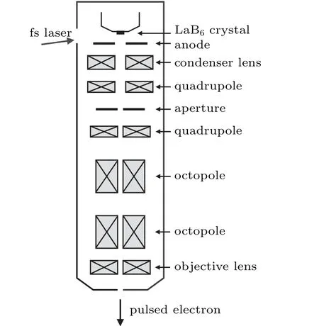
Fig.2.Schematics of the pulsed e-gun with a complex electron optics assembly.A side viewport is designed to introduce stimulation light for generation of photoemission electrons from the LaB6 photocathode.Two quadrupoles are designed to collimate the e-beam through downstream electron optics,and two octopoles are designed to reshape the e-beam profile.
Given that the temporal resolution of UED is set by the temporal width of pump laser pulse and electron pulse,and the temporal mismatch due to the velocity discrepancy between the two pulses,[5,14]our complex design of electron optics assembly is a trade-off between the desirable capability and the available temporal resolution.The temporal width of the electron pulse is mainly determined by the strength of extraction field and the length of travel pathway of electron pulse.[13,14]The temporal mismatch depends on the geometrical arrangement of the two pulses,and the probe area,i.e.,the footprint of the electron pulse impinging on the sample.We managed the pathway length in the e-gun column relatively short as~327 mm.Benefit from the two-lens design,a tight focusing of~100µm spot diameter for parallel beam is achieved at the location of~50 mm away from the e-gun end.When the photoelectron emission is tuned to contain less than one thousand electrons per pulse,we estimate an overall temporal resolution of sub-picosecond in dynamics measurements for the built MMUED,which will be demonstrated in Section 3.
2.3.Multiple operation modes of MMUED
In Fig.3 we illustrate typical applications of MMUED and the corresponding sample morphology and diffraction feature.
The most common use of UED is to probe samples in a transmission geometry with parallel incidence,as depicted in Figs.3(a)and 3(b)for samples of polycrystal thin film and single crystal membrane,generating Debye–Scherer rings,and Bragg spots,respectively.Expanding the incidence angle enables UED to probe structural dynamics of single crystal bulk sample with a convergent beam generating Kikuchi bands or line pairs,as depicted in Fig.3(c).The spanned wave vectors of convergent beam overcome the limitation of single incident wave vector of parallel beam,by an Ewald sphere with effective thickness in the reciprocal space to simultaneously map out more crystallographic directions of a unit cell.The nature of Kikuchi diffraction originated inside the region far away from sample surface,at where the diffused probe electrons are secondary scattered,brings higher spatial sensitivity in terms of detecting lattice deformations,compared to Bragg diffraction by parallel beam incidence,[53]rendering UED with convergent beam specific potentials in studies of dynamics of strain engineering or heat rectification.

Fig.3.Typical applications of MMUED and the corresponding sample morphology and diffraction feature.Red arrows and green arrows represent the pump laser beams and the probe e-beams,respectively.(a)–(c)Transmission configurations for samples of polycrystalline thin film,single crystal membrane,and single crystal bulk flake,respectively.The green triangle in panel(c)denotes the convergent e-beam impacting the sample.(d)–(f)Reflection configurations for samples of cleaned surface with adsorbate,orientated nano-crystallites on substrate,and randomly distributed nano-crystallites on substrate,respectively.The red ovals denote the tilted pump pulses,see text for details.
In a reflection geometry,UED is able to investigate samples with morphology not accessible to the transmission configuration.Samples in transmission configuration are mounted and orientated in a geometry that the normal of sample surface is parallel to the pathway of e-beam,so that the e-beam probes samples perpendicularly.To operate UED in reflection configuration,samples are mounted and orientated in a geometry that the sample surface is almost parallel to the pathway of e-beam,so that the e-beam probes samples with a grazing angle.In Fig.3(d),the e-beam impacts the sample surface with a tangential incidence,generating diffraction relrods due to very shallow region probed.Accompanied with the utilities implemented in the preparation chamber,as discussed in Subsection 2.1,this operation mode makes MMUED suitable to monitor structural changes in a very localized region started from the sample surface,and the adsorbate on top of substrate surface.[59,60]In cases that samples are nano-crystalized structures grown on a substrate,the e-beam actually probes the region of interest with a transmission incidence,although the experimental setup is in a reflection configuration,as illustrated in Figs.3(e)and 3(f)for crystallites with aligned orientation and random orientation,generating Bragg spots and Debye–Scherer rings,respectively.It is noted that only a half-set of the diffraction pattern is accessible to the detector in cases of Figs.3(e)and 3(f)because of blocking by the substrate.In order to record high order diffraction features in reflection configuration,a wedge shaped flange is inserted between the egun and the diffraction chamber,so that the propagation pathway of e-beam deviates~1°from the axis of detector,pointing the direct beam to the side area of the detector instead of the center in transmission configuration.Another drawback of reflection configuration is that the grazing angle elongates the footprint on sample surface,causing a severe temporal degradation due to the effect of group velocity mismatch between electron and laser pulses,e.g.,a footprint of 30-keV electrons traveling in the speed of 0.33 c yields 10.1-ps/mm dispersion of time zero along the direction of e-beam pathway for a typical grazing angle of 1°.To overcome the degradation of velocity mismatch,a tilting scheme of pump laser is needed in reflection configurations to alter the intensity distribution of laser pulses,so that the sample is excited precisely at the same time regards to the arrival of electrons at the probed area.[56,61]
3.Demonstrations of experimental result
In this section we demonstrate the temporal characteristics,the tunable size of probe spot,and patterns in reflection configuration of the built MMUED apparatus.Figure 4(a)shows the initial change of diffraction feature of 1T′molybdenum ditelluride(MoTe2)upon excitation of femtosecond laser with 1028-nm wavelength and~200-fs pulse duration.The sample is a mechanically peeled membrane of single crystal.As depicted in Fig.4(a),the peak height averaged over the(020)Bragg spot rapidly decreases as a function of delay time between excitation pulses and electron pulses,yielding a time constant of 1.1 ps by a mono-exponential fit.The rapid change of Bragg spot is indicative to the ultrafast process of electrons coupling their extra energy gained from excitation photons to phonons in MoTe2.More details of the study will be reported elsewhere.
In Figs.4(b)and 4(c),the static diffraction patterns recorded by pulsed electrons change as the probe spot sizes are changed by the modulation of electron optics.The sample is a polycrystalline graphene film with few layers.When a voltage of 7 kV is applied to the objective lens,the size of e-beam spot is large enough to cover adequate graphene grains to form Debye–Scherer rings in Fig.4(b).When the voltage applied to the objective lens is 9 kV,two sets of Bragg spot from the same sample area probed in Fig.4(b)are clearly formed in Fig.4(c),indicating the shrunken e-beam spot covers only a few grains.The tunable e-beam spot size provides possible distinction of phases of heterostructure sample with different grain sizes.
Figures 4(d)and 4(e)show diffraction streaks from a sapphire surface by MMUED in reflection configuration.Rotations in polar and azimuthal axes provide precise alignments for diffraction conditions in reflection mode.In Fig.4(e),another crystallographic direction comes into the in-phase condition compared to the pattern in Fig.4(d),when the sample is slightly rotated.
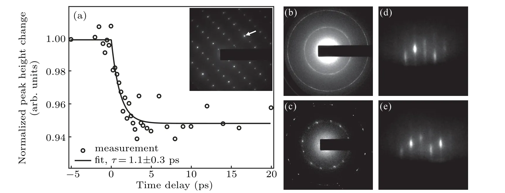
Fig.4.Ultrafast change of Bragg spot of 1T′MoTe2,diffraction feature changes of patterns in transmission mode for polycrystalline graphene thin film and reflection mode for surface of single crystal sapphire.(a)The normalized peak height change of(020)Bragg spot(marked by the white arrow in the inset)of MoTe2 follows excitation of femtosecond laser pulses,indicating a rapid process of electron–phonon coupling.Inset:Diffraction pattern of 1T′MoTe2 single crystal.(b)Debye–Scherer rings are formed through adequate amount of graphene grains probed by the e-beam spot with large size.(c)Bragg spots are formed through a few graphene grains when the e-beam spot shrinks.(d)and(e)Different crystallographic directions come into the in-phase diffraction condition in reflection mode.
4.Conclusion
We reported a design of UED apparatus with multiple operation modes for observations of ultrafast structural dynamics in solid materials of a wide range of morphologies covering bulk,thin film,surface,adsorbate,heterostructure,and nanostructure on substrate.The desired capabilities are achieved by implementations of the pulsed e-gun with delicate electron optics and the compact UHV chamber system optimized for both transmission and reflection diffraction geometries and integration of utilities for surface preparation.The versatility and the chosen low kinetic energy of e-beam make MMUED specifically suitable for investigations of emerging material family for energy harvest,conversion,and storage,which are developed in various morphologies and structures for diverse device strategies,and are often vulnerable to radiation of electrons with high kinetic energy.We anticipate MMUED addressing the transient state and the interplay between electron subsystem and phonon/lattice subsystem of materials,from the structural degrees of freedom,in study of many topics.
Acknowledgments
We thank Mr.Jiufeng Jia,Ms.Yun Liu,Ms.Renwen Cui,Ms.Yali Wang,Dr.Qun Li,Mr.Haowen Zhou and Ms.Bingxue Wang for their contributions to setting up the MMUED apparatus,and Mr.Tyler Ruttan for his helpful discussions during the design of pulsed e-gun.
杂志排行
Chinese Physics B的其它文章
- Multiple solutions and hysteresis in the flows driven by surface with antisymmetric velocity profile∗
- Magnetization relaxation of uniaxial anisotropic ferromagnetic particles with linear reaction dynamics driven by DC/AC magnetic field∗
- Influences of spin–orbit interaction on quantum speed limit and entanglement of spin qubits in coupled quantum dots
- Quantum multicast schemes of different quantum states via non-maximally entangled channels with multiparty involvement∗
- Magnetic and electronic properties of two-dimensional metal-organic frameworks TM3(C2NH)12*
- Preparation of a two-state mixture of ultracold fermionic atoms with balanced population subject to the unstable magnetic field∗